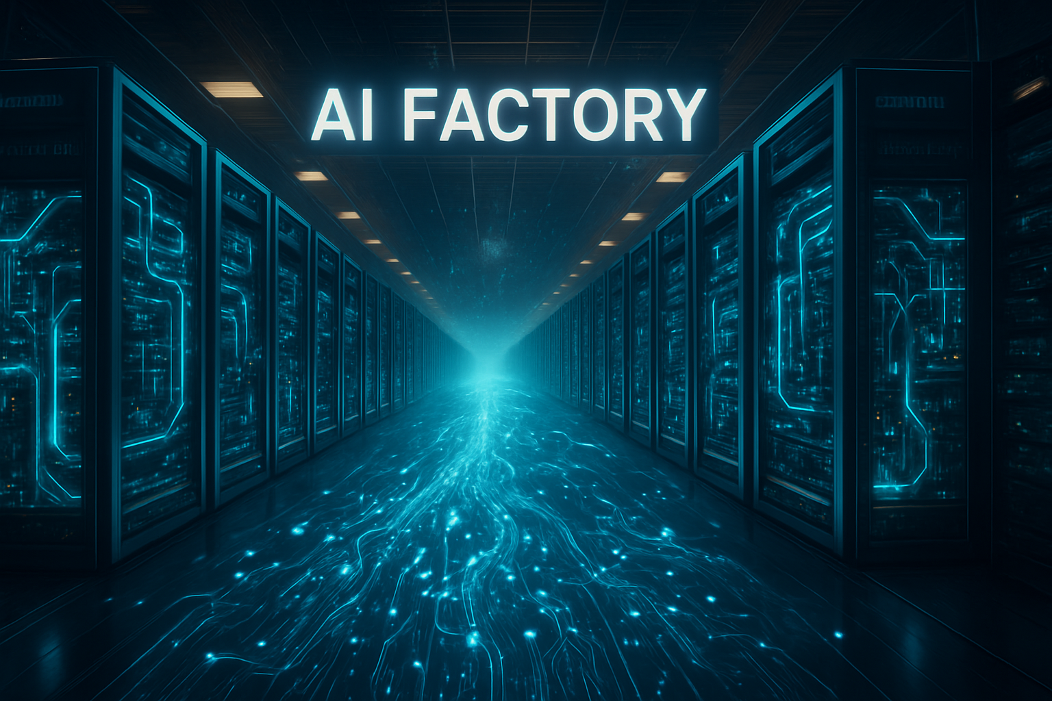
TOKYO — In a decisive move to reclaim its status as a global technology superpower, the Japanese government has officially greenlit a massive $6.34 billion (¥1 trillion) "Sovereign AI" initiative. Announced as part of the nation’s National AI Basic Plan, the funding marks a historic shift toward total technological independence, aiming to create a domestic ecosystem that encompasses everything from 2-nanometer logic chips to trillion-parameter foundational models. By 2026, the strategy has evolved from a defensive reaction to global supply chain vulnerabilities into an aggressive industrial blueprint to dominate the next phase of the "AI Industrial Revolution."
This initiative is not merely about matching the capabilities of Silicon Valley; it is a calculated effort to insulate Japan’s economy from geopolitical volatility while solving its most pressing domestic crisis: a rapidly shrinking workforce. By subsidizing the production of cutting-edge semiconductors through the state-backed venture Rapidus Corp. and fostering a "Physical AI" sector that merges machine intelligence with Japan's legendary robotics industry, the Ministry of Economy, Trade and Industry (METI) is betting that "Sovereign AI" will become the backbone of 21st-century Japanese infrastructure.
Engineering the Silicon Soul: 2nm Chips and Physical AI
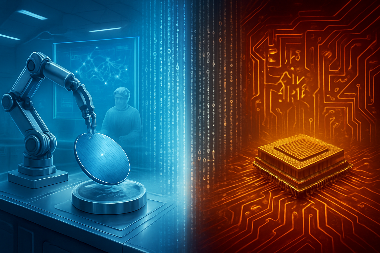
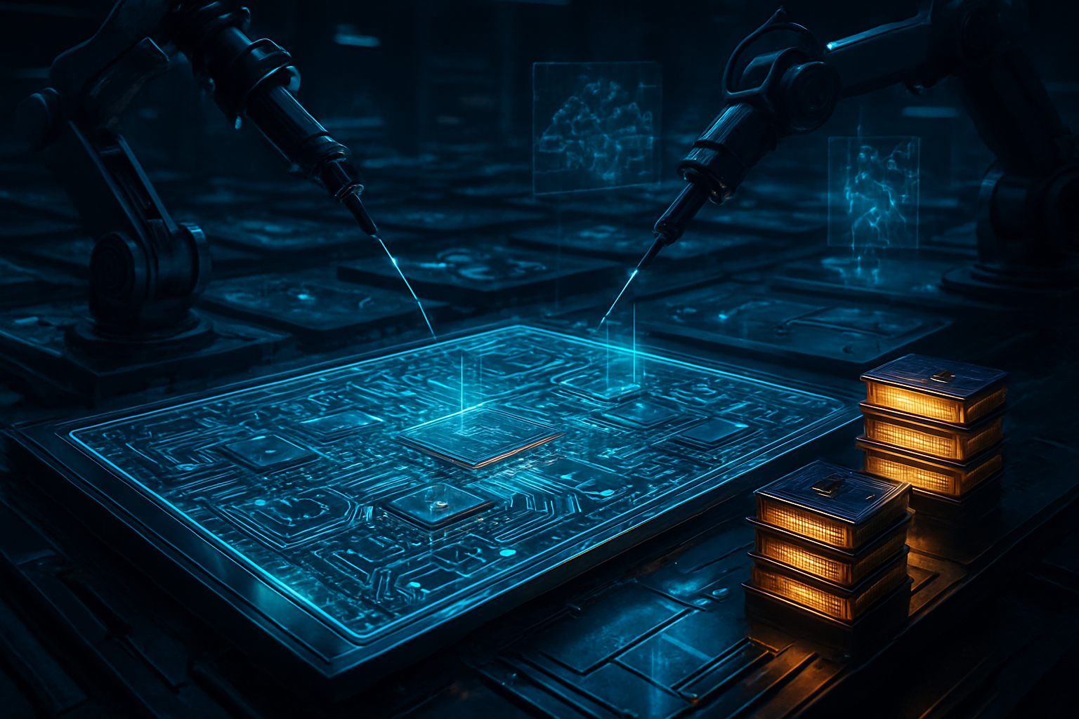
At the heart of Japan's technical roadmap is a two-pronged strategy focusing on domestic high-end manufacturing and specialized AI architectures. The centerpiece of the hardware push is Rapidus Corp., which, as of January 2026, has successfully transitioned its pilot production line in Chitose, Hokkaido, to full-wafer runs of 2-nanometer (2nm) logic chips. Unlike the traditional mass-production methods used by established foundries, Rapidus is utilizing a "single-wafer processing" approach. This allows for hyper-precise, AI-driven adjustments during the fabrication process, catering specifically to the bespoke requirements of high-performance AI accelerators rather than the commodity smartphone market.
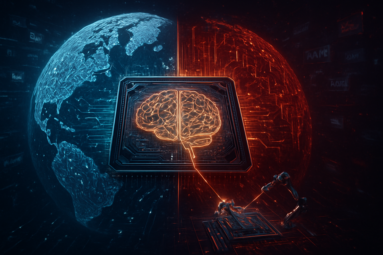
Technically, the Japanese "Sovereign AI" movement is distinguishing itself through a focus on "Physical AI" or Vision-Language-Action (VLA) models. While Western models like GPT-4 excel at digital reasoning and text generation, Japan’s national models are being trained on "physics-based" datasets and digital twins. These models are designed to predict physical torque and robotic pathing rather than just the next word in a sentence. This transition is supported by the integration of NTT’s (OTC: NTTYY) Innovative Optical and Wireless Network (IOWN), a groundbreaking photonics-based infrastructure that replaces traditional electrical signals with light, reducing latency in AI-to-robot communication to near-zero levels.
Initial reactions from the global research community have been cautiously optimistic. While some skeptics argue that Japan is starting late in the LLM race, others point to the nation’s unique data advantage. By training models on high-quality, proprietary Japanese industrial data—rather than just scraped internet text—Japan is creating a "cultural and industrial firewall." Experts at RIKEN, Japan’s largest comprehensive research institution, suggest that this focus on "embodied intelligence" could allow Japan to leapfrog the "hallucination" issues of traditional LLMs by grounding AI in the laws of physics and industrial precision.
The Corporate Battlefield: SoftBank, Rakuten, and the Global Giants
The $6 billion initiative has created a gravitational pull that is realigning Japan's corporate landscape. SoftBank Group Corp. (OTC: SFTBY) has emerged as the primary "sovereign provider," committing an additional $12.7 billion of its own capital to build massive AI data centers across Hokkaido and Osaka. These facilities, powered by the latest Blackwell architecture from NVIDIA Corporation (NASDAQ: NVDA), are designed to host "Sarashina," a 1-trillion parameter domestic model tailored for high-security government and corporate applications. SoftBank’s strategic pivot marks a transition from a global investment firm to a domestic infrastructure titan, positioning itself as the "utility provider" for Japan’s AI future.
In contrast, Rakuten Group, Inc. (OTC: RKUNY) is pursuing a strategy of "AI-nization," focusing on the edge of the network. Leveraging its virtualized 5G mobile network, Rakuten is deploying smaller, highly efficient AI models—including a 700-billion parameter LLM optimized for its ecosystem of 100 million users. While SoftBank builds the "heavyweight" backbone, Rakuten is focusing on hyper-personalized consumer AI and smart city applications, creating a competitive tension that is accelerating the adoption of AI across the Japanese retail and financial sectors.
For global giants like Taiwan Semiconductor Manufacturing Company (NYSE: TSM) and Samsung Electronics, the rise of Japan’s Rapidus represents a long-term "geopolitical insurance policy" for their customers. Major U.S. firms, including IBM (NYSE: IBM), which is a key technical partner for Rapidus, and various AI startups, are beginning to eye Japan as a secondary source for advanced logic chips. This diversification is seen as a strategic necessity to mitigate risks associated with regional tensions in the Taiwan Strait, potentially disrupting the existing foundry monopoly and giving Japan a seat at the table of advanced semiconductor manufacturing.
Geopolitics and the Sovereign AI Trend
The significance of Japan’s $6 billion investment extends far beyond its borders, signaling the rise of "AI Nationalism." In an era where data and compute power are synonymous with national security, Japan is following a global trend—also seen in France and the Middle East—of developing AI that is culturally and legally autonomous. This "Sovereign AI" movement is a direct response to concerns that a handful of U.S.-based tech giants could effectively control the "digital nervous system" of other nations, potentially leading to a new form of technological colonialism.
However, the path is fraught with potential concerns. The massive energy requirements of Japan’s planned AI factories are at odds with the country’s stringent carbon-neutrality goals. To address this, the government is coupling the AI initiative with a renewed push for next-generation nuclear and renewable energy projects. Furthermore, there are ethical debates regarding the "AI-robotics" integration. As Japan automates its elderly care and manufacturing sectors to compensate for a shrinking population, the social implications of high-density robot-human interaction remain a subject of intense scrutiny within the newly formed AI Strategic Headquarters.
Comparing this to previous milestones, such as the 1980s Fifth Generation Computer Systems project, the current Sovereign AI initiative is far more grounded in existing market demand and industrial capacity. Unlike past efforts that focused purely on academic research, the 2026 plan is deeply integrated with private sector champions like Fujitsu Ltd. (OTC: FJTSY) and the global supply chain, suggesting a higher likelihood of commercial success.
The Road to 2027: What’s Next for the Rising Sun?
Looking ahead, the next 18 to 24 months will be critical for Japan’s technological gamble. The immediate milestone is the graduation of Rapidus from pilot production to mass-market commercial viability by early 2027. If the company can achieve competitive yields on its 2nm GAA (Gate-All-Around) architecture, it will solidify Japan as a Tier-1 semiconductor player. On the software side, the release of the "Sarashina" model's enterprise API in mid-2026 is expected to trigger a wave of "AI-first" domestic startups, particularly in the fields of precision medicine and autonomous logistics.
Potential challenges include a global shortage of AI talent and the immense capital expenditure required to keep pace with the frantic development cycles of companies like OpenAI and Google. To combat this, Japan is loosening visa restrictions for "AI elites" and offering massive tax breaks for companies that repatriate their digital workloads to Japanese soil. Experts predict that if these measures succeed, Japan could become the global hub for "Embodied AI"—the point where software intelligence meets physical hardware.
A New Chapter in Technological History
Japan’s $6 billion Sovereign AI initiative represents a watershed moment in the history of artificial intelligence. By refusing to remain a mere consumer of foreign technology, Japan is attempting to rewrite the rules of the AI era, prioritizing security, cultural integrity, and industrial utility over the "move fast and break things" ethos of Silicon Valley. It is a bold, high-stakes bet that the future of AI belongs to those who can master both the silicon and the soul of the machine.
In the coming months, the industry will be watching the Hokkaido "Silicon Forest" closely. The success or failure of Rapidus’s 2nm yields and the deployment of the first large-scale Physical AI models will determine whether Japan can truly achieve technological sovereignty. For now, the "Rising Sun" of AI is ascending, and its impact will be felt across every factory floor, data center, and boardroom in the world.
This content is intended for informational purposes only and represents analysis of current AI developments.
TokenRing AI delivers enterprise-grade solutions for multi-agent AI workflow orchestration, AI-powered development tools, and seamless remote collaboration platforms.
For more information, visit https://www.tokenring.ai/.