SANTA CLARA, CA — January 13, 2026 — In a move that has effectively reset the roadmap for global computing, NVIDIA (NASDAQ:NVDA) has officially launched its Vera Rubin platform, signaling the dawn of the "Agentic AI" era. The announcement, which took center stage at CES 2026 earlier this month, comes as the company’s previous-generation Blackwell architecture reaches peak global deployment, cementing NVIDIA's role not just as a chipmaker, but as the primary architect of the world's AI infrastructure.
The dual-pronged strategy—launching the high-performance Rubin platform while simultaneously scaling the Blackwell B200 and the new B300 Ultra series—has created a near-total lock on the high-end data center market. As organizations transition from simple generative AI to complex, multi-step autonomous agents, the Vera Rubin platform’s specialized architecture is designed to provide the massive throughput and memory bandwidth required to sustain trillion-parameter models.
Engineering the Future: Inside the Vera Rubin Architecture
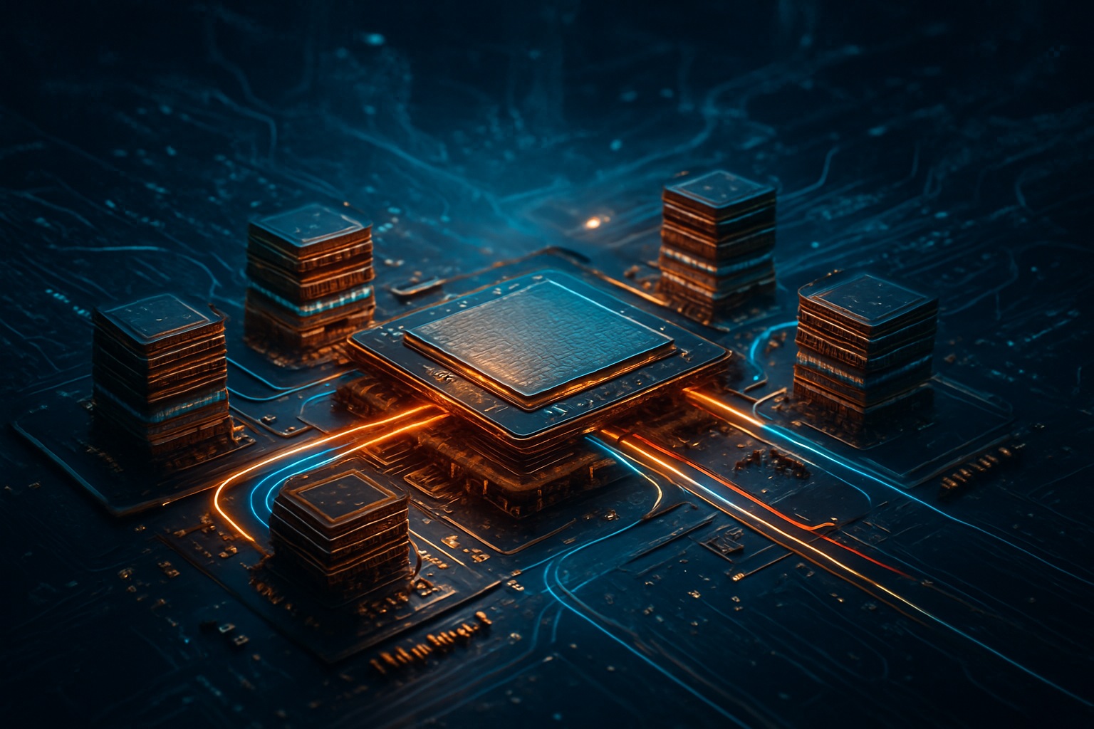
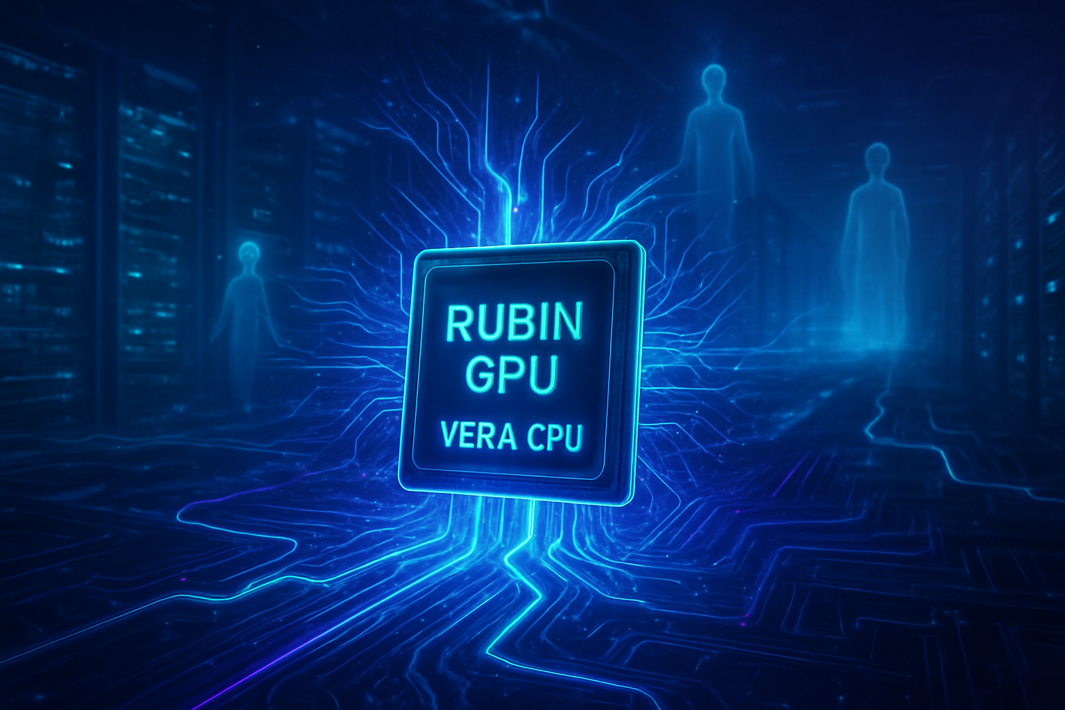
The Vera Rubin platform, anchored by the R100 GPU, represents a significant technological leap over the Blackwell series. Built on an advanced 3nm (N3P) process from Taiwan Semiconductor Manufacturing Company (NYSE:TSM), the R100 features a dual-die, reticle-limited design that delivers an unprecedented 50 Petaflops of FP4 compute. This marks a nearly 3x increase in raw performance compared to the original Blackwell B100. Perhaps more importantly, Rubin is the first platform to fully integrate the HBM4 memory standard, sporting 288GB of memory per GPU with a staggering bandwidth of up to 22 TB/s.
Beyond raw GPU power, NVIDIA has introduced the "Vera" CPU, succeeding the Grace architecture. The Vera CPU utilizes 88 custom "Olympus" Armv9.2 cores, optimized for high-velocity data orchestration. When coupled via the new NVLink 6 interconnect, which provides 3.6 TB/s of bidirectional bandwidth, the resulting NVL72 racks function as a single, unified supercomputer. This "extreme co-design" approach allows for an aggregate rack bandwidth of 260 TB/s, specifically designed to eliminate the "memory wall" that has plagued large-scale AI training for years.
The initial reaction from the AI research community has been one of awe and logistical concern. While the performance metrics suggest a path toward Artificial General Intelligence (AGI), the power requirements remain formidable. NVIDIA has mitigated some of these concerns with the ConnectX-9 SuperNIC and the BlueField-4 DPU, which introduce a new "Inference Context Memory Storage" (ICMS) tier. This allows for more efficient reuse of KV-caches, significantly lowering the energy cost per token for complex, long-context inference tasks.
Market Dominance and the Blackwell Bridge
While the Vera Rubin platform is the star of the 2026 roadmap, the Blackwell architecture remains the industry's workhorse. As of mid-January, NVIDIA’s Blackwell B100 and B200 units are essentially sold out through the second half of 2026. Tech giants like Microsoft (NASDAQ:MSFT), Meta (NASDAQ:META), Amazon (NASDAQ:AMZN), and Alphabet (NASDAQ:GOOGL) have reportedly booked the lion's share of production capacity to power their respective "AI Factories." To bridge the gap until Rubin reaches mass shipments in late 2026, NVIDIA is currently rolling out the B300 "Blackwell Ultra," featuring upgraded HBM3E memory and refined networking.
This relentless release cycle has placed intense pressure on competitors. Advanced Micro Devices (NASDAQ:AMD) is currently finding success with its Instinct MI350 series, which has gained traction among customers seeking an alternative to the NVIDIA ecosystem. AMD is expected to counter Rubin with its MI450 platform in late 2026, though analysts suggest NVIDIA currently maintains a 90% market share in the AI accelerator space. Meanwhile, Intel (NASDAQ:INTC) has pivoted toward a "hybridization" strategy, offering its Gaudi 3 and Falcon Shores chips as cost-effective alternatives for sovereign AI clouds and enterprise-specific applications.
The strategic advantage of the NVIDIA ecosystem is no longer just the silicon, but the CUDA software stack and the new MGX modular rack designs. By contributing these designs to the Open Compute Project (OCP), NVIDIA is effectively turning its proprietary hardware configurations into the global standard for data center construction. This move forces hardware competitors to either build within NVIDIA’s ecosystem or risk being left out of the rapidly standardizing AI data center blueprint.
Redefining the Data Center: The "No Chillers" Era
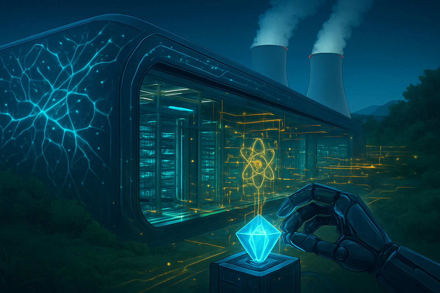
The implications of the Vera Rubin launch extend far beyond the server rack and into the physical infrastructure of the global data center. At the recent launch event, NVIDIA CEO Jensen Huang declared a shift toward "Green AI" by announcing that the Rubin platform is designed to operate with warm-water Direct Liquid Cooling (DLC) at temperatures as high as 45°C (113°F). This capability could eliminate the need for traditional water chillers in many climates, potentially reducing data center energy overhead by up to 30%.
This announcement sent shockwaves through the industrial cooling sector, with stock prices for traditional HVAC leaders like Johnson Controls (NYSE:JCI) and Trane Technologies (NYSE:TT) seeing increased volatility as investors recalibrate the future of data center cooling. The shift toward 800V DC power delivery and the move away from traditional air-cooling are now becoming the "standard" rather than the exception. This transition is critical, as typical Rubin racks are expected to consume between 120kW and 150kW of power, with future roadmaps already pointing toward 600kW "Kyber" racks by 2027.
However, this rapid advancement raises concerns regarding the digital divide and energy equity. The cost of building a "Rubin-ready" data center is orders of magnitude higher than previous generations, potentially centralizing AI power within a handful of ultra-wealthy corporations and nation-states. Furthermore, the sheer speed of the Blackwell-to-Rubin transition has led to questions about hardware longevity and the environmental impact of rapid hardware cycles.
The Horizon: From Generative to Agentic AI
Looking ahead, the Vera Rubin platform is expected to be the primary engine for the shift from chatbots to "Agentic AI"—autonomous systems that can plan, reason, and execute multi-step workflows across different software environments. Near-term applications include sophisticated autonomous scientific research, real-time global supply chain orchestration, and highly personalized digital twins for industrial manufacturing.
The next major milestone for NVIDIA will be the mass shipment of R100 GPUs in the third and fourth quarters of 2026. Experts predict that the first models trained entirely on Rubin architecture will begin to emerge in early 2027, likely exceeding the current scale of Large Language Models (LLMs) by a factor of ten. The challenge will remain the supply chain; despite TSMC’s expansion, the demand for HBM4 and 3nm wafers continues to outstrip global capacity.
A New Benchmark in Computing History
The launch of the Vera Rubin platform and the continued rollout of Blackwell mark a definitive moment in the history of computing. NVIDIA has transitioned from a company that sells chips to the architect of the global AI operating system. By vertically integrating everything from the transistor to the rack cooling system, they have set a pace that few, if any, can match.
Key takeaways for the coming months include the performance of the Blackwell Ultra B300 as a transitional product and the pace at which data center operators can upgrade their power and cooling infrastructure to meet Rubin’s specifications. As we move further into 2026, the industry will be watching closely to see if the "Rubin Revolution" can deliver on its promise of making Agentic AI a ubiquitous reality, or if the sheer physics of power and thermal management will finally slow the breakneck speed of the AI era.
This content is intended for informational purposes only and represents analysis of current AI developments.
TokenRing AI delivers enterprise-grade solutions for multi-agent AI workflow orchestration, AI-powered development tools, and seamless remote collaboration platforms.
For more information, visit https://www.tokenring.ai/.