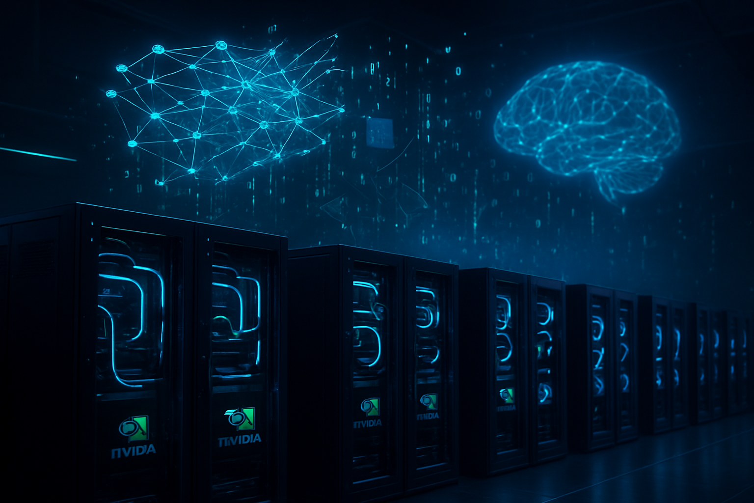
In a move that has sent shockwaves through Silicon Valley and the global corridors of power, Anthropic has finalized a historic $30 billion compute agreement with Microsoft Corp. (NASDAQ:MSFT). This unprecedented alliance, officially cemented as we enter early 2026, marks a definitive shift in the "Cloud Wars," positioning Anthropic not just as a model builder, but as a primary architect of the next industrial revolution in intelligence. By securing massive tranches of dedicated data center capacity—scaling up to a staggering one gigawatt—Anthropic has effectively locked in the computational "oxygen" required to train its next generation of frontier models, Claude 5 and beyond.
The deal is more than a simple cloud lease; it is a tripartite strategic alignment involving NVIDIA Corp. (NASDAQ:NVDA), which has contributed $10 billion to the financing alongside a $5 billion injection from Microsoft. This massive capital and infrastructure infusion values Anthropic at an eye-watering $350 billion, making it one of the most valuable private entities in history. More importantly, it grants Anthropic preferential access to NVIDIA’s most advanced silicon, transitioning from the current Grace Blackwell standard to the highly anticipated Vera Rubin architecture, which promises to break the "memory wall" that has long constrained the scaling of agentic AI.
The Silicon Foundation: From Grace Blackwell to Vera Rubin
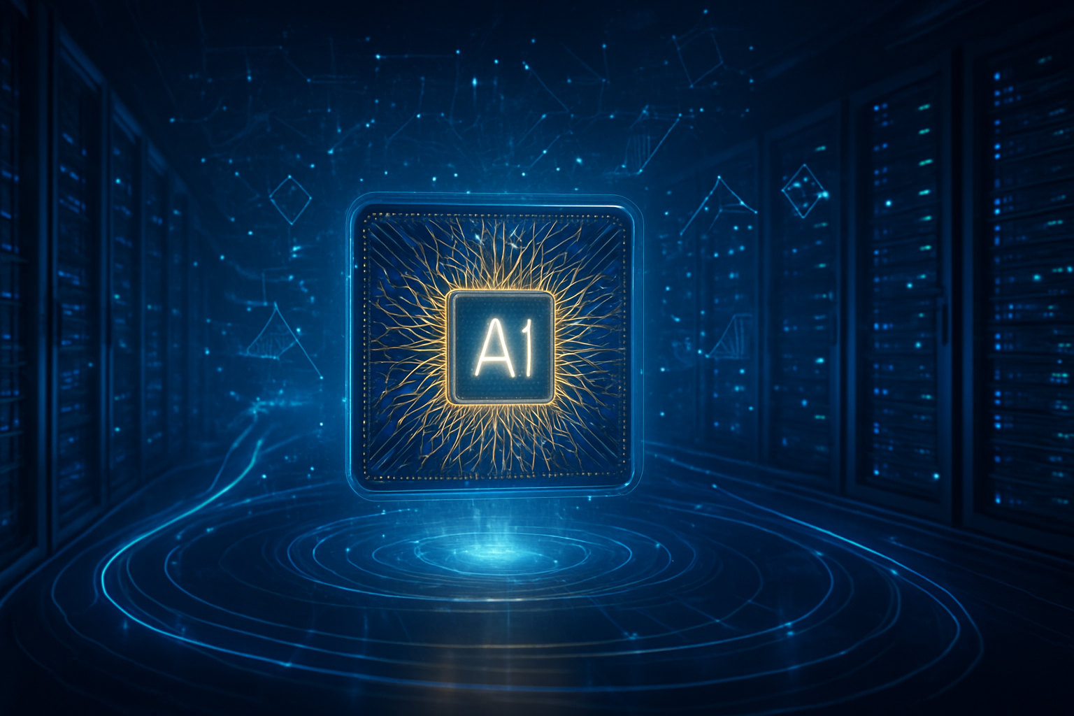
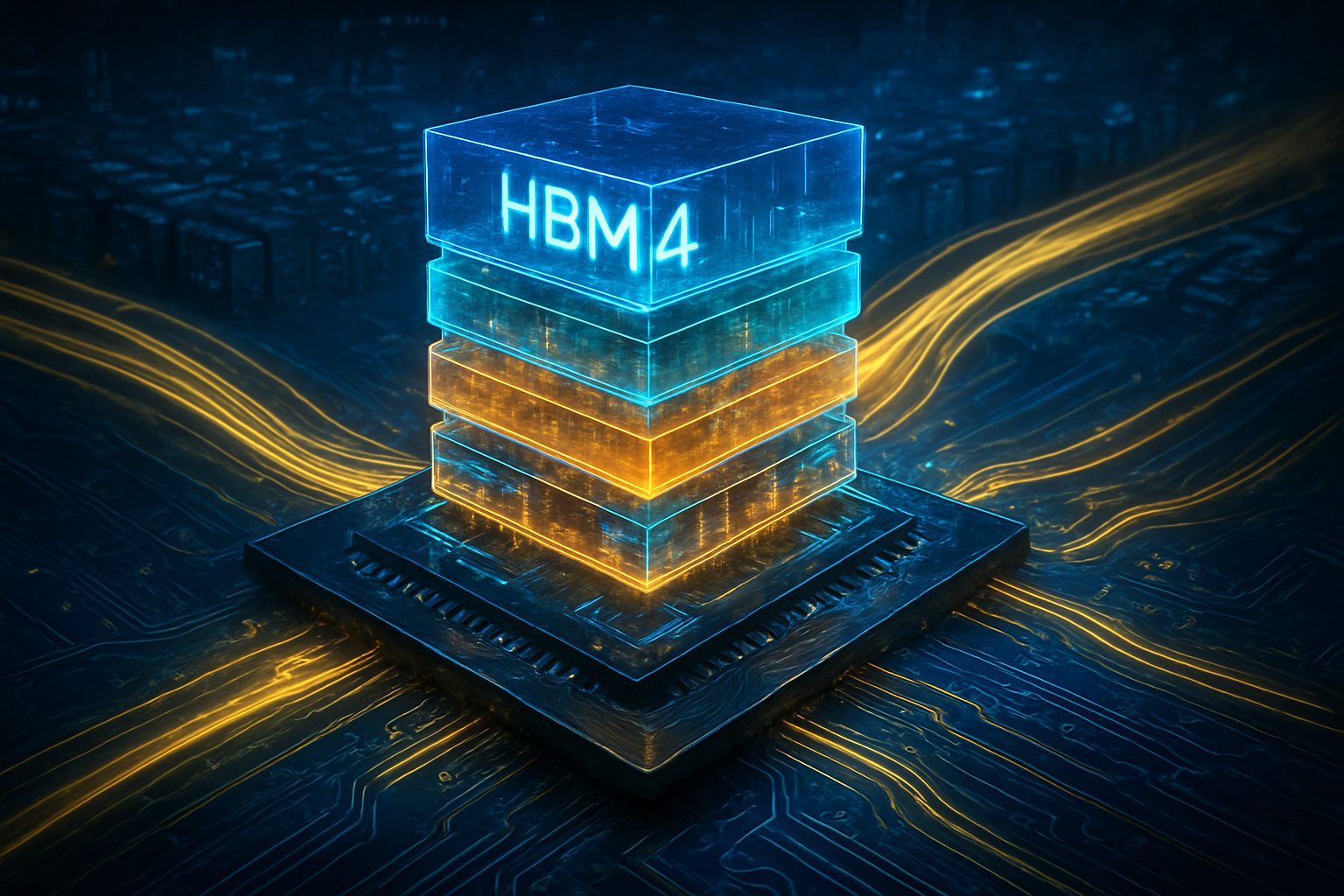
Technically, this agreement represents the first large-scale commercial commitment to NVIDIA’s Vera Rubin platform (VR200), the successor to the already formidable Blackwell architecture. While Anthropic is currently deploying its Claude 4.5 suite on Blackwell-based GB200 NVL72 systems, the $30 billion deal ensures they will be the primary launch partner for Rubin in the second half of 2026. The leap from Blackwell to Rubin is not merely incremental; it is a fundamental redesign of the AI system. The Rubin architecture introduces the "Vera" CPU, featuring 88 custom "Olympus" Arm cores designed specifically to manage the high-speed data movement required for agentic workflows, where AI must not only process information but orchestrate complex, multi-step tasks across software environments.
The technical specifications of the Vera Rubin platform are staggering. By utilizing HBM4 memory, the system delivers a memory bandwidth of 22 TB/s—a 2.8x increase over Blackwell. In terms of raw compute, the Rubin GPUs provide 50 PFLOPS of FP4 inference performance, more than doubling the capabilities of its predecessor. This massive jump in bandwidth is critical for Anthropic’s "Constitutional AI" approach, which requires significant overhead for real-time reasoning and safety checks. Industry experts note that the integration of the BlueField-4 DPU within the Rubin stack allows Anthropic to offload networking bottlenecks, potentially reducing the cost per token for large Mixture-of-Experts (MoE) models by an order of magnitude.
The Great Cloud Realignment: Microsoft’s Multi-Lab Strategy
This deal signals a profound strategic pivot for Microsoft. For years, the Redmond giant was viewed as the exclusive patron of OpenAI, but the $30 billion Anthropic deal confirms that Microsoft is diversifying its bets to mitigate "single-provider risk." By integrating Anthropic’s models into the Azure AI Foundry and Microsoft 365 Copilot, Microsoft is offering its enterprise customers a choice between the GPT and Claude ecosystems, effectively commoditizing the underlying model layer while capturing the lucrative compute margins. This move puts immense pressure on OpenAI to maintain its lead, as its primary benefactor is now actively funding and hosting its fiercest competitor.
For Anthropic, the deal completes a masterful "multi-cloud" strategy. While Amazon.com Inc. (NASDAQ:AMZN) remains a significant partner with its $8 billion investment and integration into Amazon Bedrock, and Alphabet Inc. (NASDAQ:GOOGL) continues to provide access to its massive TPU clusters, the Microsoft deal ensures that Anthropic is not beholden to any single hardware roadmap or cloud ecosystem. This "vendor neutrality" allows Anthropic to play the three cloud titans against each other, ensuring they always have access to the cheapest and most powerful silicon available, whether it be NVIDIA GPUs, Google’s TPUs, or Amazon’s Trainium chips.
The Gigawatt Era and the Industrialization of Intelligence
The scale of this agreement—specifically the mention of "one gigawatt" of power capacity—marks the beginning of the "Gigawatt Era" of AI. We are moving past the phase where AI was a software curiosity and into a phase of heavy industrialization. A single gigawatt is enough to power roughly 750,000 homes, and dedicating that much energy to a single AI lab’s compute needs underscores the sheer physical requirements of future intelligence. This development aligns with the broader trend of AI companies becoming energy players, with Anthropic now needing to navigate the complexities of nuclear power agreements and grid stability as much as neural network architectures.
However, the sheer concentration of power—both literal and metaphorical—has raised concerns among regulators and ethicists. The $30 billion price tag creates a "moat" that is virtually impossible for smaller startups to cross, potentially stifling innovation outside of the "Big Three" (OpenAI, Anthropic, and Google). Comparisons are already being made to the early days of the aerospace industry, where only a few "prime contractors" had the capital to build the next generation of jet engines. Anthropic’s move ensures they are a prime contractor in the AI age, but it also ties their destiny to the massive infrastructure of the very tech giants they once sought to provide a "safer" alternative to.
The Road to Claude 5 and Beyond
Looking ahead, the immediate focus for Anthropic will be the training of Claude 5 on the first waves of Vera Rubin hardware. Experts predict that Claude 5 will be the first model to truly master "long-horizon reasoning," capable of performing complex research and engineering tasks that span weeks rather than minutes. The increased memory bandwidth of HBM4 will allow for context windows that could theoretically encompass entire corporate codebases or libraries of legal documents, processed with near-instantaneous latency. The "Vera" CPU’s ability to handle agentic data movement suggests that the next generation of Claude will not just be a chatbot, but an autonomous operator capable of managing entire digital workflows.
The next 18 months will be a period of intense infrastructure deployment. As Microsoft builds out the dedicated "Anthropic Zones" within Azure data centers, the industry will be watching to see if the promised efficiency gains of the Rubin architecture materialize. The primary challenge will be the supply chain; even with NVIDIA’s $10 billion stake, the global demand for HBM4 and advanced 2nm logic remains at a fever pitch. Any delays in the rollout of the Vera Rubin architecture could stall Anthropic’s ambitious roadmap and give competitors a window to reclaim the narrative.
A New Epoch in the AI Arms Race
The $30 billion deal between Anthropic, Microsoft, and NVIDIA is a watershed moment that defines the landscape of artificial intelligence for the late 2020s. It represents the final transition of AI from a venture-backed software experiment into a capital-intensive infrastructure play. By securing the most advanced silicon on the planet and the power to run it, Anthropic has positioned itself as a permanent fixture in the global technological hierarchy. The significance of this development cannot be overstated; it is the moment when the "AI safety" lab fully embraced the "AI scale" reality.
In the coming months, the focus will shift from the boardroom to the data center. As the first Vera Rubin clusters come online, the true capabilities of this $30 billion investment will be revealed. For the tech industry, the message is clear: the cost of entry for frontier AI has reached the stratosphere, and the alliance between Anthropic, Microsoft, and NVIDIA has set a new, formidable standard for what it means to lead in the age of intelligence.
This content is intended for informational purposes only and represents analysis of current AI developments.
TokenRing AI delivers enterprise-grade solutions for multi-agent AI workflow orchestration, AI-powered development tools, and seamless remote collaboration platforms.
For more information, visit https://www.tokenring.ai/.