Tag: Nvidia

  • The Rubin Revolution: Nvidia’s $500 Billion Backlog Signals a New Era of AI Dominance

    The Rubin Revolution: Nvidia’s $500 Billion Backlog Signals a New Era of AI Dominance

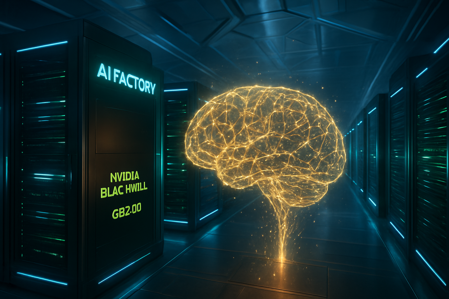
    As of February 6, 2026, the artificial intelligence landscape is bracing for its most significant hardware shift yet. NVIDIA (NASDAQ: NVDA) has officially moved its next-generation "Rubin" architecture into mass production, backed by a staggering $500 billion order backlog that underscores the insatiable global appetite for compute. This transition marks the culmination of the company’s aggressive shift to a one-year product cadence, a strategy designed to outpace competitors and cement its position as the primary architect of the AI era.

    The immediate significance of the Rubin launch cannot be overstated. With the previous Blackwell generation already powering the world's most advanced large language models (LLMs), Rubin represents a leap in efficiency and raw power that many analysts believe will unlock "agentic" AI—systems capable of autonomous reasoning and long-term planning. During a recent industry event, Nvidia CFO Colette Kress characterized the demand for this new hardware as "tremendous," noting that the primary bottleneck for the industry has shifted from chip availability to the physical capacity of energy-ready data centers.

    Engineering the Future: Inside the Rubin Architecture

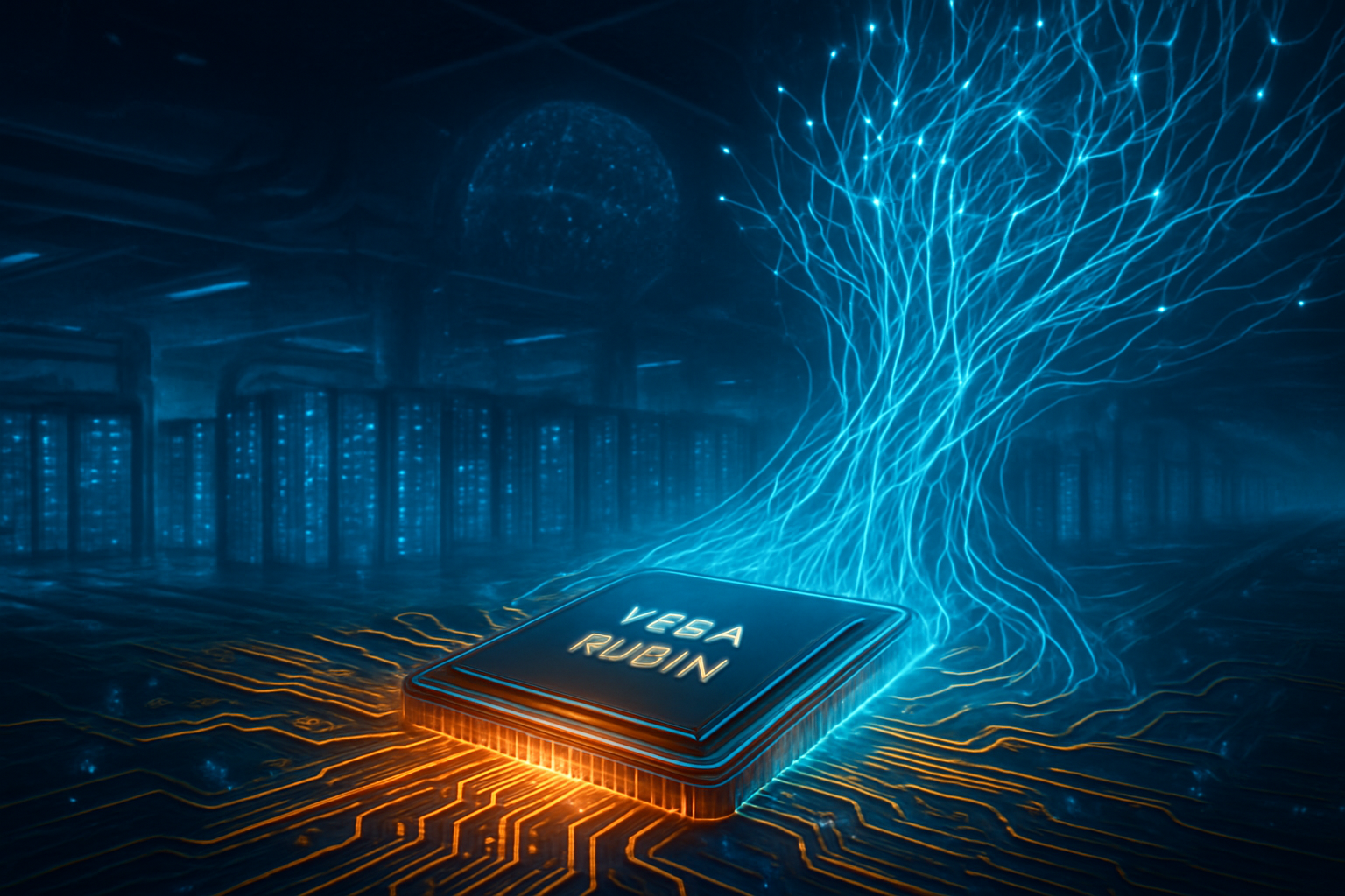
    The Rubin architecture, named after the pioneering astrophysicist Vera Rubin, represents a fundamental shift in semiconductor design. Moving from the 4nm process used in Blackwell to the cutting-edge 3nm (N3) node from Taiwan Semiconductor Manufacturing Company (NYSE: TSM), the Rubin GPU (R100) features an estimated 336 billion transistors. This density leap allows the R100 to deliver an unprecedented 50 Petaflops of NVFP4 compute—a 5x increase over its predecessor. This massive jump in performance is specifically tuned to handle the trillion-parameter models that are becoming the industry standard in 2026.

    Central to this platform is the new Vera CPU, the successor to the Grace CPU. Built on an 88-core custom Armv9.2 architecture from Arm Holdings (NASDAQ: ARM), the Vera CPU is codenamed "Olympus" and features a 1.8 TB/s NVLink-C2C interconnect. This allows for a unified memory pool where the CPU and GPU can share data with minimal latency, effectively tripling the system memory available to the GPU. Furthermore, Rubin is the first architecture to fully integrate HBM4 memory, utilizing eight stacks of high-bandwidth memory to provide a breathtaking 22.2 TB/s of bandwidth. This ensures that the massive compute power of the R100 is never starved for data, a critical requirement for real-time inference and massive-context reasoning.

    Initial reactions from the AI research community have been a mix of awe and logistical concern. Experts at leading labs note that the Rubin CPX variant, designed for "Massive Context" operations with 1M+ tokens, could finally bridge the gap between simple chatbots and truly autonomous AI agents. However, the shift to HBM4 and the 3nm node has also highlighted the complexity of the global supply chain, with Nvidia relying heavily on partners like SK Hynix (KRX: 000660) and Samsung (KRX: 005930) to meet the demanding specifications of the new memory standard.

    Market Dominance and the $500 Billion Moat

    The financial implications of the Rubin rollout are as massive as the hardware itself. Reports of a $500 billion backlog indicate that Nvidia has effectively "sold out" its production capacity well into 2027. This backlog includes orders for the current Blackwell Ultra chips and early commitments for the Rubin platform from hyperscalers like Microsoft (NASDAQ: MSFT), Meta Platforms (NASDAQ: META), and Alphabet (NASDAQ: GOOGL). By locking in these massive orders, Nvidia has created a strategic moat that makes it difficult for custom ASIC (Application-Specific Integrated Circuit) projects from Amazon (NASDAQ: AMZN) or Google to gain significant ground.

    For tech giants, the decision to invest in Rubin is a matter of survival in the AI arms race. Companies that secure the first shipments of Rubin SuperPODs in late 2026 will have a significant advantage in training the next generation of "frontier" models. Conversely, startups and smaller AI labs may find themselves increasingly reliant on cloud providers who can afford the steep entry price of Nvidia’s latest silicon. This has led to a tiered market where Rubin is used for cutting-edge training, while older architectures like Blackwell and Hopper are relegated to more cost-effective inference tasks.

    The competitive landscape is also reacting to Nvidia's "Apple-style" yearly release cycle. While some critics argue this creates "artificial obsolescence," the reality on the ground is different. Even older A100 and H100 chips remain at nearly 100% utilization across the industry. Nvidia’s strategy isn't just about replacing old chips; it's about expanding the total available compute to meet a demand curve that shows no sign of flattening. By releasing new architectures annually, Nvidia ensures that it remains the "gold standard" for every new breakthrough in AI research.

    The Wider Significance: Power, Policy, and the Jevons Paradox

    Beyond the boardroom and the data center, the Rubin architecture brings the intersection of AI and energy infrastructure into sharp focus. Each Rubin NVL72 rack is expected to draw upwards of 250kW, requiring advanced liquid cooling systems as a standard rather than an option. This highlights the "Jevons Paradox" in the AI age: as Rubin makes the cost of generating an "AI token" significantly more efficient, the resulting drop in price is driving users to run models more frequently and for more complex tasks. This increased efficiency is actually driving up total energy consumption across the globe.

    The social and political ramifications are equally significant. As Nvidia’s backlog grows, the company has become a central figure in geopolitical discussions regarding "compute sovereignty." Nations are now competing to secure their own Rubin-based sovereign AI clouds to ensure they aren't left behind in the transition to an AI-driven economy. However, the concentration of so much power—both literal and figurative—in a single hardware architecture has raised concerns about a single point of failure in the global AI ecosystem.

    Furthermore, the environmental impact of such a massive hardware rollout is under scrutiny. While Nvidia emphasizes the "performance per watt" gains of the Vera CPU and Rubin GPU, the sheer scale of the $500 billion backlog suggests a carbon footprint that will challenge the sustainability goals of many tech giants. Policymakers in early 2026 are increasingly looking at "compute-to-energy" ratios as a metric for regulating future data center expansions.

    The Horizon: From Rubin to Feynman

    Looking ahead, the roadmap for 2027 and beyond is already taking shape. Following the Rubin Ultra update expected in early 2027, Nvidia has already teased its next architectural milestone, codenamed "Feynman." While Rubin is designed to perfect the current transformer-based models, Feynman is rumored to be optimized for "World Models" and robotics, integrating even more advanced physical simulation capabilities directly into the silicon.

    The near-term challenge for Nvidia will be execution. Managing a $500 billion backlog requires a flawless supply chain and a steady hand from CFO Colette Kress and CEO Jensen Huang. Any delay in the 3nm transition or the rollout of HBM4 could create a vacuum that competitors are eager to fill. Additionally, as AI models move toward on-device execution (Edge AI), Nvidia will need to ensure that its dominance in the data center translates effectively to smaller, more power-efficient form factors.

    Experts predict that by the end of 2026, the success of the Rubin architecture will be measured not just by benchmarks, but by the complexity of the tasks AI can perform autonomously. If Rubin enables the "reasoning" breakthrough many expect, the $500 billion backlog might just be the beginning of a multi-trillion dollar infrastructure cycle.

    A Summary of the Rubin Era

    The transition to the Rubin architecture and the Vera CPU marks a definitive moment in technological history. By condensing its development cycle and pushing the limits of TSMC’s 3nm process and HBM4 memory, Nvidia has effectively decoupled itself from the traditional pace of the semiconductor industry. The $500 billion backlog is a testament to a world that views compute as the new oil—a finite, essential resource for the 21st century.

    Key takeaways for the coming months include:

    • Mass Production Readiness: Rubin is moving into full production in February 2026, with first shipments expected in the second half of the year.
    • Unified Ecosystem: The Vera CPU and NVLink-C2C integration further lock customers into the full Nvidia stack, from networking to silicon.
    • Infrastructure Constraints: The "tremendous demand" cited by Colette Kress is now limited more by power and cooling than by chip supply.

    As we move through 2026, the tech industry will be watching closely to see if the physical infrastructure of the world can keep up with Nvidia's silicon. The Rubin architecture isn't just a faster chip; it is the foundation for the next stage of artificial intelligence, and the world is already waiting in line to build on it.


    This content is intended for informational purposes only and represents analysis of current AI developments.

    TokenRing AI delivers enterprise-grade solutions for multi-agent AI workflow orchestration, AI-powered development tools, and seamless remote collaboration platforms.
    For more information, visit https://www.tokenring.ai/.

  • The $8 Trillion Math Problem: IBM CEO Arvind Krishna Warns of Impending AI Infrastructure Bubble

    The $8 Trillion Math Problem: IBM CEO Arvind Krishna Warns of Impending AI Infrastructure Bubble

    In a series of candid warnings delivered at the 2026 World Economic Forum in Davos and during recent high-profile interviews, IBM (NYSE: IBM) Chairman and CEO Arvind Krishna has sounded the alarm on what he calls the "$8 trillion math problem." Krishna argues that the current global trajectory of capital expenditure on artificial intelligence infrastructure has reached a point of financial unsustainability, potentially leading to a massive economic correction for tech giants and investors alike.

    While Krishna remains a staunch believer in the underlying value of generative AI technology, he distinguishes between the "real productivity gains" of the software and the "speculative fever" driving massive data center construction. According to Krishna, the industry is currently locked in a "brute-force" arms race that ignores the fundamental laws of accounting, specifically regarding the rapid depreciation of AI hardware and the astronomical costs of servicing the debt required to build it.

    The Depreciation Trap and the 100-Gigawatt Goal

    At the heart of Krishna’s warning is a detailed breakdown of the costs associated with the global push toward Artificial General Intelligence (AGI). Krishna estimates that the industry’s current goal is to build approximately 100 gigawatts (GW) of total AI-class compute capacity globally. With high-end accelerators, specialized liquid cooling, and power infrastructure now costing roughly $80 billion per gigawatt, the total bill for this build-out reaches a staggering $8 trillion.

    This figure becomes problematic when combined with what Krishna calls the "Depreciation Trap." Unlike traditional infrastructure like bridges or power plants, which might be amortized over 30 to 50 years, AI accelerators have a functional competitive lifecycle of only five years. This means that every five years, the $8 trillion investment must be effectively "refilled" as old hardware becomes obsolete. Furthermore, at a conservative 10% corporate borrowing rate, servicing the interest on an $8 trillion debt would require $800 billion in annual profit—a figure that currently exceeds the combined net income of the world’s largest technology companies.

    This technical and financial reality differs sharply from the "spend-at-all-costs" mentality that characterized the early 2020s. Initial reactions from the AI research community have been split; while some hardware-focused analysts defend the spending as necessary for the "scaling laws" of LLMs, many financial experts and enterprise researchers are beginning to side with Krishna’s call for "fit-for-purpose" AI that requires significantly less compute.

    Hyperscalers in the Crosshairs: A Strategic Shift

    The implications of Krishna’s "math problem" are most profound for the "hyperscalers"—Microsoft (NASDAQ: MSFT), Alphabet (NASDAQ: GOOGL), Meta (NASDAQ: META), and Amazon (NASDAQ: AMZN). These companies have historically been the primary beneficiaries of the AI boom, alongside NVIDIA (NASDAQ: NVDA), but they now face a critical pivot. If Krishna is correct, the strategic advantage of having the largest data center may soon be outweighed by the massive financial drag of maintaining it.

    IBM is positioning itself as the alternative to this "massive model" philosophy. In its Q4 2025 earnings report, IBM revealed a generative AI book of business worth $12.5 billion, focused largely on software, consulting, and domain-specific models rather than massive infrastructure. This suggests a market shift where startups and enterprise labs may stop trying to out-scale the giants and instead focus on "Agentic" workflows—highly efficient, specialized AI agents that perform specific business tasks without needing trillion-parameter models.

    For major AI labs like OpenAI, the sustainability of their current trajectory is under intense scrutiny. If the capital required for the next generation of models continues to grow exponentially without a corresponding explosion in revenue, the industry could see a wave of consolidation or a cooling of the venture capital landscape, similar to the post-2000 tech crash.

    Beyond the Bubble: Productivity vs. Speculation

    Krishna is careful to clarify that while the infrastructure may be in a bubble, the technology itself is not. He compares the current moment to the build-out of fiber-optic cables during the late 1990s; while many of the companies that laid the cable went bankrupt, the internet itself remained and fundamentally changed the world. He views the pursuit of AGI—which he estimates has only a 0% to 1% chance of success with current architectures—as a speculative venture that has obscured the immediate, tangible benefits of AI.

    The wider significance lies in the potential impact on global energy and environmental goals. The 100 GW of capacity Krishna cites would consume more power than many medium-sized nations, raising concerns about the environmental cost of speculative compute. By highlighting the $8 trillion hurdle, Krishna is forcing a conversation about whether the "brute-force scaling" of the last few years is a viable path forward for a world increasingly focused on energy efficiency and sustainable growth.

    This discourse represents a maturation of the AI era. We are moving from a period of "AI wonder" into a period of "AI accountability," where CEOs and CFOs are no longer satisfied with impressive demos and are instead demanding clear paths to ROI that account for the massive CapEx requirements.

    The Rise of Agentic AI and Domain-Specific Models

    Looking ahead, experts predict 2026 will be the year of "compute cooling." As the $8 trillion math problem becomes harder to ignore, the focus is expected to shift toward model optimization, quantization, and "on-device" AI. Near-term developments will likely focus on "Agentic" AI—systems that don't just generate text but autonomously execute complex multi-step workflows. These systems are often more efficient because they use smaller, specialized models tailored for specific industries like law, medicine, or engineering.

    The challenge for the next 24 months will be bridging the gap between the $200–$300 billion current AI services market and the $800 billion interest burden Krishna identified. To close this gap, AI must move beyond chatbots and into the core of enterprise operations. Predictions for 2027 suggest a massive "thinning of the herd" among AI startups, with only those providing measurable, high-margin utility surviving the transition from the infrastructure build-out phase to the application value phase.

    Final Assessment: A Reality Check for the AI Era

    Arvind Krishna’s $8 trillion warning serves as a significant milestone in the history of artificial intelligence. It marks the moment when the industry’s largest players began to confront the physical and financial limits of scaling. While the potential for a 10x productivity revolution remains real—with Krishna himself predicting AI could eventually automate 50% of back-office roles—the path to that future cannot be paved with unlimited capital.

    The key takeaway is that the "infrastructure bubble" is a cautionary tale of over-extrapolation, not a death knell for the technology. As we move into the middle of 2026, the industry should be watched for a shift in narrative from "how many GPUs do you have?" to "how much value can you create per watt?" The companies that thrive will be those that solve the math problem by making AI smaller, smarter, and more sustainable.


    This content is intended for informational purposes only and represents analysis of current AI developments.

    TokenRing AI delivers enterprise-grade solutions for multi-agent AI workflow orchestration, AI-powered development tools, and seamless remote collaboration platforms.
    For more information, visit https://www.tokenring.ai/.

  • The Open-Source Revolution: How Meta’s Llama Series Erased the Proprietary AI Advantage

    The Open-Source Revolution: How Meta’s Llama Series Erased the Proprietary AI Advantage

    In a shift that has fundamentally altered the trajectory of Silicon Valley, the gap between "walled-garden" artificial intelligence and open-weights models has effectively vanished. What began with the disruptive launch of Meta’s Llama 3.1 405B in 2024 has evolved into a new era of "Superintelligence" with the 2025 rollout of the Llama 4 series. Today, as of February 2026, the AI landscape is no longer defined by the exclusivity of proprietary labs, but by a democratized ecosystem where the most powerful models are increasingly available for download and local deployment.

    Meta Platforms Inc. (NASDAQ: META) has successfully positioned itself as the architect of this new world order. By releasing high-frontier models that rival and occasionally surpass the performance of offerings from OpenAI and Google (Alphabet Inc. (NASDAQ: GOOGL)), Meta has broken the monopoly on state-of-the-art AI. The implications are profound: enterprises that once feared vendor lock-in are now building on Llama’s "open" foundations, forcing a radical shift in how AI value is captured and monetized across the industry.

    The Technical Leap: From Dense Giants to Efficient 'Herds'

    The foundation of this shift was the Llama 3.1 405B, which, upon its release in late 2024, became the first open-weights model to match GPT-4o and Claude 3.5 Sonnet in core reasoning and coding benchmarks. Trained on a staggering 15.6 trillion tokens using a fleet of 16,000 Nvidia (NASDAQ: NVDA) H100 GPUs, the 405B model proved that massive dense architectures could be successfully distilled into smaller, highly efficient 8B and 70B variants. This "distillation" capability allowed developers to leverage the "teacher" model's intelligence to create lightweight "students" tailored for specific enterprise tasks—a practice previously blocked by the terms of service of proprietary providers.

    However, the real technical breakthrough arrived in April 2025 with the Llama 4 series, known internally as the "Llama Herd." Moving away from the dense architecture of Llama 3, Meta adopted a highly sophisticated Mixture-of-Experts (MoE) framework. The flagship "Maverick" model, with 400 billion total parameters (but only 17 billion active during any single inference), currently sits at the top of the LMSys Chatbot Arena. Perhaps even more impressive is the "Scout" variant, which introduced a 10-million-token context window, allowing the model to ingest entire codebases or libraries of legal documents in a single prompt—surpassing the capabilities of Google’s Gemini 2.0 series in long-context retrieval (RULER) benchmarks.

    This technical evolution was made possible by Meta’s unprecedented investment in compute infrastructure. By early 2026, Meta’s GPU fleet has grown to over 1.5 million units, heavily featuring Nvidia’s Blackwell B200 and GB200 "Superchips." This massive compute moat allowed Meta to train its latest research preview, "Behemoth"—a 2-trillion-parameter MoE model—which aims to pioneer "agentic" AI. Unlike its predecessors, Llama 4 is designed with native hooks for autonomous web browsing, code execution, and multi-step workflow orchestration, transforming the model from a passive responder into an active digital employee.

    A Seismic Shift in the Competitive Landscape

    Meta’s "open-weights" strategy has created a strategic paradox for its rivals. While Microsoft (NASDAQ: MSFT) and OpenAI have relied on a high-margin, API-only business model, Meta’s decision to give away the "crown jewels" has commoditized the underlying intelligence. This has been a boon for startups and mid-sized enterprises, which can now deploy frontier-level AI on their own private clouds or local hardware, avoiding the data privacy concerns and high costs associated with proprietary APIs. For these companies, Meta has become the "Linux of AI," providing a standard, customizable foundation that everyone else builds upon.

    The competitive pressure has triggered a pricing war among AI service providers. To compete with the "free" weights of Llama 4, proprietary labs have been forced to slash API prices and accelerate their release cycles. Meanwhile, cloud providers like Amazon (NASDAQ: AMZN) and Google have had to pivot, focusing more on providing the specialized infrastructure (like specialized Llama-optimized instances) rather than just selling their own proprietary models. Meta, in turn, is monetizing not through the models themselves, but through "agentic commerce" integrated into WhatsApp and Instagram, as well as by becoming the primary AI platform for sovereign governments that demand local control over their intelligence infrastructure.

    Furthermore, Meta is beginning to reduce its dependence on external hardware through its Meta Training and Inference Accelerator (MTIA) program. While Nvidia remains a critical partner, the deployment of MTIA v2 for ranking and recommendation tasks—and the upcoming MTIA v3 built on a 3nm process—signals Meta’s intent to control the entire stack. By optimizing Llama 4 to run natively on its own silicon, Meta is creating a vertical integration that could eventually offer a performance-per-watt advantage that even the largest proprietary labs will struggle to match.

    Global Significance and the Ethics of Openness

    The rise of Llama has reignited the global debate over AI safety and national security. Proponents of the open-weights model argue that democratization is the best defense against AI monopolies, allowing researchers worldwide to inspect the weights for biases and vulnerabilities. This transparency has led to a surge in "community-driven safety," where independent researchers have developed robust guardrails for Llama 4 far faster than any single company could have done internally.

    However, this openness has also drawn scrutiny from regulators and security hawks. Critics argue that releasing the weights of models as powerful as Llama 4 Behemoth could allow bad actors to strip away safety filters, potentially enabling the creation of biological weapons or sophisticated cyberattacks. Meta has countered this by implementing a "Semi-Open" licensing model; while the weights are accessible, the Llama Community License restricts use for companies with more than 700 million monthly active users, preventing rivals like ByteDance from using Meta’s research to gain a competitive edge.

    The broader significance of the Llama series lies in its role as a "great equalizer." In 2026, we are seeing the emergence of "Sovereign AI," where nations like France, India, and the UAE are using Llama as the backbone for national AI initiatives. This prevents a future where global intelligence is controlled by a handful of companies in San Francisco. By making frontier AI a public good (with caveats), Meta has effectively shifted the "AI Divide" from a question of who has the model to a question of who has the compute and the data to apply it.

    The Horizon: Llama 4 Behemoth and the MTIA Era

    Looking ahead to the remainder of 2026, the industry is focused on the full public release of Llama 4 Behemoth. Currently in limited research preview, Behemoth is expected to be the first open-weights model to achieve "Expert-Level" reasoning across all scientific and mathematical benchmarks. Experts predict that its release will mark the beginning of the "Agentic Era," where AI agents will handle everything from personal scheduling to complex software engineering with minimal human oversight.

    The next frontier for Meta is the integration of its in-house MTIA v3 silicon with these massive models. If Meta can successfully migrate Llama 4 inference from expensive Nvidia GPUs to its own more efficient chips, the cost of running state-of-the-art AI could drop by another order of magnitude. This would enable "AI at the edge" on a scale previously thought impossible, with high-intelligence models running locally on smart glasses and mobile devices without relying on the cloud.

    The primary challenges remaining are not just technical, but legal and social. The ongoing litigation regarding the use of copyrighted data for training continues to loom over the entire industry. How Meta navigates these legal waters—and how it addresses the "fudged benchmark" controversies that surfaced in early 2026—will determine whether Llama remains the trusted standard for the open AI community or if a new competitor, perhaps from the decentralized AI movement, rises to take its place.

    Summary: A New Paradigm for Artificial Intelligence

    The journey from Llama 3.1 405B to the Llama 4 herd represents one of the most significant pivots in the history of technology. By choosing a path of relative openness, Meta has not only caught up to the proprietary leaders but has fundamentally redefined the rules of the game. The "gap" is no longer about raw intelligence; it is about application, integration, and the scale of compute.

    As we move further into 2026, the key takeaway is that the "moat" of proprietary intelligence has evaporated. The significance of this development cannot be overstated—it has accelerated AI adoption, decentralized power, and forced every major tech player to rethink their strategy. In the coming months, all eyes will be on the performance of Llama 4 Behemoth and the rollout of Meta’s custom silicon. The era of the AI monopoly is over; the era of the open frontier has begun.


    This content is intended for informational purposes only and represents analysis of current AI developments.

    TokenRing AI delivers enterprise-grade solutions for multi-agent AI workflow orchestration, AI-powered development tools, and seamless remote collaboration platforms.
    For more information, visit https://www.tokenring.ai/.

  • NVIDIA Blackwell B200 and GB200 Chips Enter Volume Production: Fueling the Trillion-Parameter AI Era

    NVIDIA Blackwell B200 and GB200 Chips Enter Volume Production: Fueling the Trillion-Parameter AI Era

    SANTA CLARA, CA — As of February 5, 2026, the global landscape of artificial intelligence has reached a critical inflection point. NVIDIA (NASDAQ: NVDA) has officially moved its Blackwell architecture—specifically the B200 GPU and the liquid-cooled GB200 NVL72 rack system—into full-scale volume production. This transition marks the end of the "scarcity era" that defined 2024 and 2025, providing the raw computational horsepower necessary to train and deploy the next generation of frontier AI models, including OpenAI’s highly anticipated GPT-5 and its subsequent iterations.

    The ramp-up in production is bolstered by a historic milestone: TSMC (NYSE: TSM) has successfully reached high-yield parity at its Fab 21 facility in Arizona. For the first time, NVIDIA’s most advanced 4NP process silicon is being produced in massive quantities on U.S. soil, significantly de-risking the supply chain for North American tech giants. With over 3.6 million units already backlogged by major cloud providers, the Blackwell era is not just an incremental upgrade; it represents the birth of the "AI Factory" as the new standard for industrial-scale intelligence.

    The Blackwell B200 is a marvel of semiconductor engineering, moving away from the monolithic designs of the past toward a sophisticated dual-die chiplet architecture. Each B200 houses a staggering 208 billion transistors, effectively functioning as a single, seamless processor through a 10 TB/s interconnect. This design allows for a massive leap in memory capacity, with the standard B200 now featuring 192GB of HBM3e memory and a bandwidth of 8 TB/s. These specs represent a nearly 2.4x increase over the previous H100 "Hopper" generation, which reigned supreme throughout 2023 and 2024.

    A key technical breakthrough that has the research community buzzing is the second-generation Transformer Engine, which introduces support for FP4 precision. By utilizing 4-bit floating-point arithmetic without sacrificing significant accuracy, the Blackwell platform delivers up to 20 PFLOPS of peak performance. In practical terms, this allows researchers to serve models with 15x to 30x higher throughput than the Hopper architecture. This shift to FP4 is considered the "secret sauce" that will make the real-time operation of trillion-parameter models economically viable for the general public.

    Beyond the individual chip, the GB200 NVL72 system has redefined data center architecture. By connecting 72 Blackwell GPUs into a single unified domain via the 5th-Gen NVLink, NVIDIA has created a "rack-scale GPU" with 130 TB/s of aggregate bandwidth. This interconnect speed is crucial for models like GPT-5, which are rumored to exceed 1.8 trillion parameters. In these environments, the bottleneck is often the communication between chips; Blackwell’s NVLink 5 eliminates this, treating the entire rack as a single computational entity.

    The shift to volume production has massive implications for the "Big Three" cloud providers and the labs they support. Microsoft (NASDAQ: MSFT) has been the first to deploy tens of thousands of Blackwell units per month across its "Fairwater" AI superfactories. These facilities are specifically designed to handle the 100kW+ power density required by liquid-cooled Blackwell racks. For Microsoft and OpenAI, this infrastructure is the foundation for GPT-5, enabling the model to process context windows in the millions of tokens while maintaining the reasoning speeds required for autonomous agentic behavior.

    Amazon (NASDAQ: AMZN) and its AWS division have similarly aggressive roadmaps, recently announcing the general availability of P6e-GB200 UltraServers. AWS has notably implemented its own proprietary In-Row Heat Exchanger (IRHX) technology to manage the extreme thermal output of these chips. By providing Blackwell-tier compute at scale, AWS is positioning itself to be the primary host for the next wave of "sovereign AI" projects—national-level initiatives where countries like Japan and the UK are building their own LLMs to ensure data privacy and cultural alignment.

    The competitive advantage for companies that can secure Blackwell silicon is currently insurmountable. Startups and mid-tier AI labs that are still relying on H100 clusters are finding it difficult to compete on training efficiency. According to recent benchmarks, training a 1.8-trillion parameter model requires 8,000 Hopper GPUs and 15 MW of power, whereas the Blackwell platform can accomplish the same task with just 2,000 GPUs and 4 MW. This 4x reduction in hardware footprint and power consumption has fundamentally changed the venture capital math for AI startups, favoring those with "Blackwell-ready" infrastructure.

    Looking at the broader AI landscape, the Blackwell ramp-up signifies a transition from "brute force" scaling to "rack-scale efficiency." For years, the industry worried about the "power wall"—the idea that we would run out of electricity before we could reach AGI. Blackwell’s energy efficiency suggests that we can continue to scale model complexity without a linear increase in power consumption. This development is crucial as the industry moves toward "Agentic AI," where models don't just answer questions but perform complex, multi-step tasks in the real world.

    However, the concentration of Blackwell chips in the hands of a few tech titans has raised concerns about a growing "compute divide." While NVIDIA's increased production helps, the backlog into mid-2026 suggests that only the wealthiest organizations will have access to the peak of AI performance for the foreseeable future. This has led to renewed calls for decentralized compute initiatives and government-funded "national AI clouds" to ensure that academic researchers aren't left behind by the private sector's massive AI factories.

    The environmental impact remains a double-edged sword. While Blackwell is more efficient per TFLOP, the sheer scale of the deployments—some data centers are now crossing the 500 MW threshold—continues to put pressure on global energy grids. The industry is responding with a massive push into small modular reactors (SMRs) and direct-to-chip liquid cooling, but the "AI energy crisis" remains a primary topic of discussion at global tech summits in early 2026.

    Looking ahead, NVIDIA is not resting on its laurels. Even as the B200 reaches volume production, the first shipments of the "Blackwell Ultra" (B300) have begun, featuring an even larger 288GB HBM3e memory pool. This mid-cycle refresh is designed to bridge the gap until the arrival of the "Rubin" architecture, slated for late 2026 or early 2027. Rubin is expected to introduce even more advanced 3nm process nodes and a shift toward HBM4 memory, signaling that the pace of hardware innovation shows no signs of slowing.

    In the near term, we expect to see the "inference explosion." Now that the hardware exists to serve trillion-parameter models efficiently, we will see these capabilities integrated into every facet of consumer technology, from operating systems that can predict user needs to real-time, high-fidelity digital twins for industrial manufacturing. The challenge will shift from "how do we train these models" to "how do we govern them," as agentic AI begins to handle financial transactions, legal analysis, and healthcare diagnostics autonomously.

    The mass production of Blackwell B200 and GB200 chips represents a landmark moment in the history of computing. Much like the introduction of the first mainframes or the birth of the internet, this deployment provides the infrastructure for a new era of human productivity. NVIDIA has successfully transitioned from being a component maker to the primary architect of the world's most powerful "AI factories," solidifying its position at the center of the 21st-century economy.

    As we move through the first half of 2026, the key metric to watch will be the "token-to-watt" ratio. The true success of Blackwell will not just be measured in TFLOPS, but in how it enables AI to become a ubiquitous, affordable utility. With GPT-5 on the horizon and the hardware finally in place to support it, the next few months will likely see the most significant leaps in AI capability we have ever witnessed.


    This content is intended for informational purposes only and represents analysis of current AI developments.

    TokenRing AI delivers enterprise-grade solutions for multi-agent AI workflow orchestration, AI-powered development tools, and seamless remote collaboration platforms.
    For more information, visit https://www.tokenring.ai/.

  • The DeepSeek Disruption: How R1’s $6 Million Breakthrough Shattered the AI Brute-Force Myth

    The DeepSeek Disruption: How R1’s $6 Million Breakthrough Shattered the AI Brute-Force Myth

    In January 2025, a relatively obscure laboratory in Hangzhou, China, released a model that sent shockwaves through Silicon Valley, effectively ending the era of "brute-force" scaling. DeepSeek-R1 arrived not with the multi-billion-dollar fanfare of a traditional frontier release, but with a startling technical claim: it could match the reasoning capabilities of OpenAI’s top-tier models for a fraction of the cost. By February 2026, the industry has come to recognize this release as a "Sputnik Moment," one that fundamentally altered the economic trajectory of artificial intelligence and sparked the "Efficiency Revolution" currently defining the tech landscape.

    The immediate significance of DeepSeek-R1 lay in its price-to-performance ratio. While Western giants like Microsoft (NASDAQ: MSFT) and Google (NASDAQ: GOOGL) were pouring tens of billions into massive GPU clusters, DeepSeek-R1 was trained for an estimated $6 million. This wasn't just a marginal improvement; it was a total demolition of the established scaling laws that suggested intelligence was strictly a function of compute and capital. In the year since its debut, the "DeepSeek effect" has forced every major AI lab to pivot from "bigger is better" to "smarter is cheaper," a shift that remains the central theme of the industry as of early 2026.

    Architecture of a Revolution: How Sparsity Beat Scale

    DeepSeek-R1’s dominance was built on three technical pillars: Mixture-of-Experts (MoE) sparsity, Group Relative Policy Optimization (GRPO), and Multi-Head Latent Attention (MLA). Unlike traditional dense models that activate every parameter for every query, the DeepSeek architecture—totaling 671 billion parameters—only activates 37 billion parameters per token. This "sparse" approach allows the model to maintain the high-level intelligence of a massive system while operating with the speed and efficiency of a much smaller one. This differs significantly from the previous approaches of labs that relied on massive, monolithic dense models, which suffered from high latency and astronomical inference costs.

    The most discussed innovation, however, was GRPO. While traditional reinforcement learning (RL) techniques like PPO require a separate "critic" model to monitor and reward the AI’s behavior—a process that doubles the memory and compute requirement—GRPO calculates rewards relative to a group of generated outputs. This algorithmic shortcut allowed DeepSeek to train complex reasoning pipelines on a budget that most Silicon Valley startups would consider "seed round" funding. Initial reactions from the AI research community were a mix of awe and skepticism, with many initially doubting the $6 million figure until the model’s open-weights release allowed independent researchers to verify its staggering efficiency.

    The DeepSeek Rout: Market Shocks and the End of Excessive Spend

    The release caused what financial analysts now call the "DeepSeek Rout." On January 27, 2025, NVIDIA (NASDAQ: NVDA) experienced a historic single-day loss of nearly $600 billion in market capitalization as investors panicked over the prospect that AI efficiency might lead to a sharp decline in GPU demand. The ripples were felt across the entire semiconductor supply chain, hitting Broadcom (NASDAQ: AVGO) and ASML (NASDAQ: ASML) as the "brute-force" narrative—the idea that the world needed an infinite supply of H100s to achieve AGI—began to crack.

    By February 2026, the business implications have crystallized. Major AI labs have been forced into a pricing war. OpenAI and Google have repeatedly slashed API costs to match the "DeepSeek Standard," which currently sees DeepSeek-V3.2 (released in January 2026) offering reasoning capabilities comparable to GPT-5.2 at one-tenth the price. This commoditization has benefited startups and enterprise users but has severely strained the margins of the "God-model" builders. The recent collapse of the rumored $100 billion infrastructure deal between NVIDIA and OpenAI in late 2025 is seen as a direct consequence of this shift; investors are no longer willing to fund "circular" infrastructure spending when efficiency-focused models are achieving the same results with far less hardware.

    Redefining Scaling Laws: The Shift to Test-Time Efficiency

    DeepSeek-R1's true legacy is its validation of "Test-Time Scaling." Rather than just making the model larger during the training phase, DeepSeek proved that a model can become "smarter" during the inference phase by "thinking longer"—generating internal chains of thought to solve complex problems. This shifted the focus of the entire industry toward reasoning-per-watt. It was a milestone comparable to the release of GPT-4, but instead of proving that AI could do anything, it proved that AI could do anything efficiently.

    This development also brought potential concerns to the forefront, particularly regarding the depletion of high-quality public training data. As the industry entered the "Post-Scaling Era" in late 2025, the realization set in that the "brute-force" method of scraping the entire internet had reached a point of diminishing returns. DeepSeek’s success using reinforcement learning and synthetic reasoning traces provided a roadmap for how the industry could continue to advance even after hitting the "data wall." However, this has also led to a more competitive and secretive environment regarding the "cold-start" datasets used to prime these efficient models.

    The Roadmap to 2027: Agents, V4, and the Sustainable Compute Gap

    Looking toward the remainder of 2026 and into 2027, the focus has shifted from simple chatbots to agentic workflows. However, the industry is currently weathering what some call an "Agentic Winter." While DeepSeek-R1 and its successors are highly efficient at reasoning, the real-world application of autonomous agents has proved more difficult than anticipated. Experts predict that the next breakthrough will not come from more compute, but from better "world models" that allow these efficient systems to interact more reliably with physical and digital environments.

    The upcoming release of DeepSeek-V4, rumored for mid-2026, is expected to introduce an "Engram" memory architecture designed specifically for long-term agentic autonomy. Meanwhile, Western labs are racing to bridge the "sustainable compute gap," trying to match DeepSeek’s efficiency while maintaining the safety guardrails that are often more computationally expensive to implement. The challenge for the next year will be balancing the drive for lower costs with the need for robust, reliable AI that can operate without human oversight in high-stakes industries like healthcare and finance.

    A New Baseline for the Intelligence Era

    DeepSeek-R1 did more than just release a new model; it reset the baseline for the entire AI industry. It proved that the "Sovereign AI" movement—where nations and smaller entities build their own frontier models—is economically viable. The key takeaway from the last year is that architectural ingenuity is a more powerful force than raw capital. In the history of AI, DeepSeek-R1 will likely be remembered as the model that ended the "Gold Rush" phase of AI infrastructure and ushered in the "Industrialization" phase, where efficiency and ROI are the primary metrics of success.

    As we move through February 2026, the watchword is "sobering efficiency." The market has largely recovered from the initial shocks, but the demand for "brute-force" compute has been permanently replaced by a demand for "quant-optimized" intelligence. The coming months will be defined by how the legacy tech giants adapt to this new reality—and whether they can reclaim the efficiency lead from the lab that turned the AI world upside down for just $6 million.


    This content is intended for informational purposes only and represents analysis of current AI developments.

    TokenRing AI delivers enterprise-grade solutions for multi-agent AI workflow orchestration, AI-powered development tools, and seamless remote collaboration platforms.
    For more information, visit https://www.tokenring.ai/.

  • The Infrastructure Imperative: Inside Nvidia’s Massive $20 Billion Bet to Anchor OpenAI’s $830 Billion Empire

    The Infrastructure Imperative: Inside Nvidia’s Massive $20 Billion Bet to Anchor OpenAI’s $830 Billion Empire

    In a move that cements the "circular economy" of the artificial intelligence era, Nvidia (NASDAQ:NVDA) has finalized a staggering $20 billion investment in OpenAI as part of a broader $100 billion funding round. This infusion, confirmed this week in February 2026, values the San Francisco-based AI pioneer at approximately $830 billion—catapulting it into a rare stratosphere of valuation occupied by only a handful of the world’s most powerful corporations.

    The deal marks a significant strategic pivot for Nvidia. No longer content with merely being the primary "arms dealer" of the AI revolution, Nvidia is now its most foundational financier. By taking a direct equity stake in its largest customer, Nvidia is ensuring that the massive, multi-gigawatt data centers required for the next generation of "Agentic AI" will be built almost exclusively on its proprietary architecture. This $20 billion commitment serves as a massive backstop for OpenAI’s ambitious infrastructure roadmap, providing the liquidity needed to transition from research-heavy operations to a dominant global utility.

    The Vera Rubin Era and the $100 Billion War Chest

    The technical core of this investment is inextricably linked to the rollout of Nvidia’s newest architecture, the "Vera Rubin" platform. Named after the pioneering astronomer, the Rubin GPU and Vera CPU represent the next leap in compute density, with a single rack capable of delivering 8 exaflops of AI performance. OpenAI’s commitment to this hardware is the bedrock of the deal. The $20 billion cash-for-equity transaction replaces a previously discussed $100 billion infrastructure partnership, which analysts say was scaled back to a more "straightforward" stake after internal concerns at Nvidia regarding OpenAI’s fiscal discipline and its flirtation with rival chip startups like Groq and Cerebras.

    Initial reactions from the AI research community have been a mix of awe and apprehension. While researchers are eager to see what the massive scale of the Vera Rubin platform can do for GPT-6 and beyond, industry experts like those at Radio Free Mobile have raised alarms about "circular funding." They argue that Nvidia is effectively lending money to its own customer base to ensure they can afford to buy its chips, a feedback loop that could mask underlying market saturation. However, with OpenAI’s revenue projected to hit $25 billion in 2026—up from $13 billion in 2025—the company argues that the capital is backed by real-world enterprise demand rather than speculation.

    Securing the Supply Chain Against Rising Rivals

    This investment creates a formidable moat for both parties. For OpenAI, the $830 billion valuation provides the leverage needed to negotiate massive power and land deals for its "10-Gigawatt Initiative"—a plan to build "AI factories" that could rival the energy consumption of mid-sized nations. For Nvidia, the deal ensures that its silicon remains the industry standard at a time when Amazon (NASDAQ:AMZN) and Google (NASDAQ:GOOGL) are increasingly pushing their own custom Trainium and TPU chips. By becoming a primary owner of OpenAI, Nvidia effectively locks in its most influential customer for the foreseeable future.

    The competitive landscape is shifting rapidly. While Microsoft (NASDAQ:MSFT) remains OpenAI's largest stakeholder with roughly 27% equity, the entry of Nvidia as a multi-billion dollar shareholder introduces a new dynamic. Amazon has also been in talks to contribute as much as $50 billion to this round, seeking a multi-vendor strategy that would integrate OpenAI’s models into AWS while maintaining its own hardware independence. This high-stakes maneuvering has left smaller AI labs and startups in a precarious position, as the capital required to compete at the "frontier" level has now reached the hundreds of billions, effectively pricing out all but the most well-funded tech giants.

    The Global AI Factory: Trends and Concerns

    Beyond the immediate financial figures, the Nvidia-OpenAI deal signifies the emergence of the "AI Factory" as the new unit of industrial power. We are moving away from the era of "models as products" and into "compute as an economy." This shift fits into a broader trend where AI labs are evolving into vertically integrated infrastructure providers. The massive scale of this funding round mirrors previous industrial milestones, such as the build-out of the global telecommunications network in the late 1990s, but with a much faster rate of capital deployment.

    However, the sheer size of the $830 billion valuation raises concerns about a potential "compute bubble." If the transition to "Agentic AI"—models that can autonomously execute workflows and manage enterprise tasks—fails to deliver the expected productivity gains, the entire ecosystem could face a liquidity crisis. Furthermore, the reliance on Middle Eastern sovereign wealth funds and massive debt-to-equity swaps to fund these 10-gigawatt data centers has prompted calls for more transparency regarding the environmental impact and the concentration of AI power within a handful of boardroom circles.

    Toward a Trillion-Dollar IPO and Beyond

    Looking ahead, this funding round is widely viewed as the final "pre-IPO" benchmark. Sources close to OpenAI suggest the company is preparing for a public listing as early as late 2026, with a target valuation exceeding $1 trillion. The near-term focus will be on the successful deployment of "Project Stargate," the first massive-scale data center resulting from this collaboration. If successful, it will enable a new class of AI agents capable of handling complex multi-step reasoning, from software engineering to scientific discovery, with minimal human intervention.

    The challenges remaining are largely physical. Solving the energy constraints of these massive "AI factories" and optimizing inference performance are top priorities. While OpenAI has relied on Nvidia for training, it continues to explore specialized silicon for inference tasks to reduce the exorbitant cost of running its models. How Nvidia responds to OpenAI’s continued research into rival hardware will be the next major test of this multi-billion dollar marriage of convenience.

    A New Chapter in Computing History

    Nvidia’s $20 billion investment in OpenAI is more than just a financial transaction; it is a declaration of the new world order in technology. It marks the moment when the world’s most valuable chipmaker decided that its future was too important to be left to the whims of its customers' balance sheets. By anchoring the $830 billion OpenAI empire, Nvidia has ensured that it remains at the center of the AI story for the next decade.

    The key takeaways from this historic deal are clear: the cost of entry for frontier AI is now measured in the hundreds of billions, and the line between hardware vendor and platform owner has permanently blurred. In the coming months, the industry will be watching the first benchmarks of the Vera Rubin-powered GPT models and monitoring whether the projected revenue growth can justify the astronomical valuations. For now, the Nvidia-OpenAI alliance stands as the most powerful force in the history of computing.


    This content is intended for informational purposes only and represents analysis of current AI developments.

    TokenRing AI delivers enterprise-grade solutions for multi-agent AI workflow orchestration, AI-powered development tools, and seamless remote collaboration platforms.
    For more information, visit https://www.tokenring.ai/.

  • The Open Architecture Revolution: RISC-V Claims the High Ground as NVIDIA Ships One Billion Cores

    The Open Architecture Revolution: RISC-V Claims the High Ground as NVIDIA Ships One Billion Cores

    The semiconductor landscape has reached a historic turning point. As of February 2026, the once-unshakeable duopoly of x86 and ARM is facing its most significant challenge yet from RISC-V, the open-standard Instruction Set Architecture (ISA). What began as an academic project at UC Berkeley has matured into a cornerstone of high-end computing, driven by a massive surge in industrial adoption and sovereign government backing.

    The most striking evidence of this shift comes from NVIDIA (NASDAQ: NVDA), which has officially crossed the milestone of shipping over one billion RISC-V cores. These are not merely secondary components; they are critical to the operation of the world's most advanced AI and graphics hardware. This milestone, paired with the European Union’s aggressive €270 million investment into the architecture, signals that RISC-V has moved beyond the "internet of things" (IoT) and is now a dominant force in the high-performance computing (HPC) and data center markets.

    Technical Mastery: How NVIDIA Orchestrates Complexity via RISC-V

    NVIDIA’s transition to RISC-V represents a profound shift in how modern GPUs are managed. By February 2026, the company has successfully integrated custom RISC-V microcontrollers across its entire high-end portfolio, including the Blackwell and newly launched Vera Rubin architectures. These chips no longer rely on the proprietary "Falcon" controllers of the past. Instead, each high-end GPU now houses between 10 and 40 specialized RISC-V cores. These include the NV-RISCV32 for simple control logic, the NV-RISCV64—a 64-bit out-of-order, dual-issue core for heavy management—and the high-performance NV-RVV, which utilizes a 1024-bit vector extension to handle data-heavy internal telemetry.

    These cores are the unsung heroes of AI performance, managing critical functions like Secure Boot and Authentication, which form the hardware root-of-trust essential for secure multi-tenant data centers. They also handle fine-grained Power Regulation, adjusting voltage and thermal limits at microsecond intervals to squeeze every ounce of performance from the silicon while preventing thermal throttling. Perhaps most importantly, the RISC-V-based GPU System Processor (GSP) offloads complex kernel driver tasks from the host CPU. By handling these functions locally on the GPU using the open architecture, NVIDIA has drastically reduced latency and overhead, allowing its AI accelerators to communicate more efficiently across massive NVLink clusters.

    Strategic Disruption: The End of the x86 and ARM Hegemony

    This architectural shift is sending shockwaves through the corporate boardrooms of Silicon Valley. Tech giants such as Meta Platforms, Inc. (NASDAQ: META), Alphabet Inc. (NASDAQ: GOOGL), and Qualcomm (NASDAQ: QCOM) have significantly pivoted their R&D toward RISC-V to gain "architectural sovereignty." Unlike ARM’s licensing model, which historically restricted the addition of custom instructions, RISC-V allows these companies to build bespoke silicon tailored to their specific AI workloads without paying the "ARM Tax" or being tethered to a single vendor’s roadmap.

    The competitive implications for Intel (NASDAQ: INTC) and Advanced Micro Devices (NASDAQ: AMD) are stark. While x86 remains the incumbent for legacy server applications, the high-growth "bespoke silicon" market—where hyperscalers build their own chips—is rapidly trending toward RISC-V. Companies like Tenstorrent, led by industry veteran Jim Keller, have already commercialized accelerators like the Blackhole AI chip, featuring 768 RISC-V cores. These chips are being adopted by AI startups as cost-effective alternatives to mainstream hardware, leveraging the open-source nature of the ISA to innovate faster than traditional proprietary cycles allow.

    Geopolitical Sovereignty: Europe’s €270 Million Bet on Autonomy

    Beyond the corporate race, the surge of RISC-V is a matter of geopolitical strategy. The European Union has committed €270 million through the EuroHPC Joint Undertaking to build a self-sustaining RISC-V ecosystem. This investment is the bedrock of the EU Chips Act, designed to ensure that European infrastructure is no longer solely dependent on U.S. or UK-controlled technologies. By February 2026, this initiative has already yielded results, such as the Technical University of Munich’s (TUM) announcement of the first European-designed 7nm neuromorphic AI chip based on RISC-V.

    This movement toward "technological sovereignty" is more than just a defensive measure; it is a full-scale offensive. Projects like TRISTAN and ISOLDE have standardized industrial-grade RISC-V IP for the automotive and industrial sectors, creating a verified "European core" that competes directly with ARM’s Cortex-A series. For the first time in decades, Europe has a viable path to architectural independence, significantly reducing the risk of being caught in the crossfire of international trade disputes or export controls. In this context, RISC-V is becoming the "Linux of hardware"—a neutral, high-performance foundation that no single nation or company can turn off.

    The Horizon: AI Fusion Cores and the Road to 2030

    The future of RISC-V in the high-end market appears even more ambitious. The industry is currently moving toward the "RVA23" enterprise standard, which will bring even greater parity with high-end ARM Neoverse and x86 server chips. New entrants like SpacemiT and Ventana Micro Systems are already sampling server-class processors with up to 192 cores per socket, aiming for the 3.6GHz performance threshold required for hyperscale environments. We are also seeing the emergence of "AI Fusion" cores, where RISC-V CPU instructions and AI matrix math are integrated into a single pipeline, potentially simplifying the programming model for the next generation of generative AI models.

    However, challenges remain. While the hardware is maturing rapidly, the software ecosystem—though bolstered by the RISE (RISC-V Software Ecosystem) initiative—still has gaps in specific enterprise applications and high-end gaming. Experts predict that the next 24 months will be a "software sprint," where the community works to ensure that every major Linux distribution, compiler, and database is fully optimized for the unique vector extensions that RISC-V offers. If the current trajectory continues, the architecture is expected to capture over 25% of the total data center market by the end of the decade.

    A New Era for Computing

    The milestone of one billion cores at NVIDIA and the strategic backing of the European Union represent a permanent shift in the semiconductor power dynamic. RISC-V is no longer an underdog; it is a tier-one architecture that provides the flexibility, security, and performance required for the AI era. By breaking the duopoly of x86 and ARM, it has introduced a level of competition and innovation that the industry has not seen in over thirty years.

    As we look ahead, the significance of this development in AI history cannot be overstated. It represents the democratization of high-performance silicon design. In the coming weeks and months, watch for more major cloud providers to announce their own custom RISC-V "cobalt-class" processors and for further updates on the integration of RISC-V into consumer-grade high-end electronics. The era of the open ISA is here, and it is reshaping the world one core at a time.


    This content is intended for informational purposes only and represents analysis of current AI developments.

    TokenRing AI delivers enterprise-grade solutions for multi-agent AI workflow orchestration, AI-powered development tools, and seamless remote collaboration platforms.
    For more information, visit https://www.tokenring.ai/.

  • Silicon Sovereignty: Meta Charges Into 2026 with ‘Iris’ MTIA Rollout and Rapid Custom Chip Roadmap

    Silicon Sovereignty: Meta Charges Into 2026 with ‘Iris’ MTIA Rollout and Rapid Custom Chip Roadmap

    In a definitive move to secure its infrastructure against the volatile fluctuations of the global semiconductor market, Meta Platforms, Inc. (NASDAQ: META) has accelerated the deployment of its third-generation custom silicon, the Meta Training and Inference Accelerator (MTIA) v3, codenamed "Iris." As of February 2026, the Iris chips have moved into broad deployment across Meta’s massive data center fleet, signaling a pivotal shift from the company's historical reliance on general-purpose hardware. This rollout is not merely a hardware upgrade; it represents Meta’s full-scale transition into a vertically integrated AI powerhouse capable of designing, building, and optimizing the very atoms that power its algorithms.

    The immediate significance of the Iris rollout lies in its specialized architecture, which is custom-tuned to manage the staggering scale of recommendation systems behind Facebook Reels and Instagram. By moving away from off-the-shelf solutions, Meta has reported a transformative 40% to 44% reduction in total cost of ownership (TCO) for its AI infrastructure. With an aggressive roadmap that includes the MTIA v4 "Santa Barbara," the v5 "Olympus," and the v6 "Universal Core" already slated for 2026 through 2028, Meta is effectively decoupling its future from the "GPU famine" of years past, positioning itself as a primary architect of the next decade's AI hardware standards.

    Technical Deep Dive: The 'Iris' Architecture and the 2026 Roadmap

    The MTIA v3 "Iris" represents a generational leap over its predecessors, Artemis (v2) and Freya (v1). Fabricated on the cutting-edge 3nm process from Taiwan Semiconductor Manufacturing Company (NYSE: TSM), Iris is designed to solve the "memory wall" that often bottlenecks AI performance. It integrates eight HBM3E 12-high memory stacks, delivering a bandwidth exceeding 3.5 TB/s. Unlike general-purpose GPUs from NVIDIA Corporation (NASDAQ: NVDA), which are designed for a broad array of mathematical tasks, Iris features a specialized 8×8 matrix computing architecture and a sparse computing pipeline. This is specifically optimized for Deep Learning Recommendation Models (DLRM), which spend the vast majority of their compute cycles on embedding table lookups and ranking funnels.

    Meta has also introduced a specialized sub-variant of the Iris generation known as "Arke," an inference-only chip developed in collaboration with Marvell Technology, Inc. (NASDAQ: MRVL). While the flagship Iris was designed primarily with assistance from Broadcom Inc. (NASDAQ: AVGO), the Arke variant represents a strategic diversification of Meta’s supply chain. Looking ahead to the latter half of 2026, Meta is readying the MTIA v4 "Santa Barbara" for deployment. This upcoming generation is expected to move beyond air-cooled racks to advanced liquid-cooling systems, supporting high-density configurations that exceed 180kW per rack. The v4 chips will reportedly be the first to integrate HBM4 memory, further widening the throughput for the massive, multi-trillion parameter models currently in development.

    Strategic Impact on the Semiconductor Industry and AI Titans

    The aggressive scaling of the MTIA program has sent ripples through the semiconductor industry, specifically impacting the "Inference War." While Meta remains one of the largest buyers of NVIDIA’s Blackwell and Rubin GPUs for training its frontier Llama models, it is rapidly moving its inference workloads—which represent the bulk of its daily operational costs—to internal silicon. Analysts suggest that by the end of 2026, Meta aims to have over 35% of its total inference fleet running on MTIA hardware. This shift significantly reduces NVIDIA’s addressable market for high-volume, "standard" social media AI tasks, forcing the GPU giant to pivot toward more flexible, general-purpose software moats like the CUDA ecosystem.

    Conversely, the MTIA program has become a massive revenue tailwind for Broadcom and Marvell. Broadcom, acting as Meta’s structural architect, has seen its AI-related revenue projections soar, driven by the custom ASIC (Application-Specific Integrated Circuit) trend. For Meta, the strategic advantage is two-fold: cost efficiency and hardware-software co-design. By controlling the entire stack—from the PyTorch framework to the silicon itself—Meta can implement optimizations that are physically impossible on closed-source hardware. This includes custom memory management that allows Instagram’s algorithms to process over 1,000 concurrent machine learning models per user session without the latency spikes that typically lead to user attrition.

    Broader Significance: The Era of Domain-Specific AI Architectures

    The rollout of Iris and the 2026 roadmap highlight a broader trend in the AI landscape: the transition from general-purpose "one-size-fits-all" hardware to domain-specific architectures (DSAs). Meta’s move mirrors similar efforts by Google and Amazon, but with a specific focus on the unique demands of social media. Recommendation engines require massive data movement and sparse matrix math rather than the raw FP64 precision needed for scientific simulations. By stripping away unnecessary components and focusing on integer and 16-bit operations, Meta is proving that efficiency—measured in performance-per-watt—is the ultimate currency in the race for AI supremacy.

    However, this transition is not without concerns. The immense power requirements of the 2026 "Santa Barbara" clusters raise questions about the long-term sustainability of Meta’s data center growth. As chips become more specialized, the industry risks a fragmentation of software standards. Meta is countering this by ensuring MTIA is fully integrated with PyTorch, an open-source framework it pioneered, but the technical debt of maintaining a custom hardware-software stack is a hurdle few companies other than the "Magnificent Seven" can clear. This could potentially widen the gap between tech giants and smaller startups that lack the capital to build their own silicon.

    Future Outlook: From Recommendation to Universal Intelligence

    As we look toward the tail end of 2026 and into 2027, the MTIA program is expected to evolve from a specialized recommendation engine into a "Universal AI Core." The upcoming MTIA v5 "Olympus" is rumored to be Meta’s first attempt at a 2nm chiplet-based architecture. This generation is designed to handle both high-end training for future "Llama 5" and "Llama 6" models and real-time inference, potentially replacing NVIDIA’s role in Meta’s training clusters entirely. Industry insiders predict that v5 will feature Co-Packaged Optics (CPO), allowing for lightning-fast inter-chip communication that bypasses traditional copper bottlenecks.

    The primary challenge moving forward will be the transition to these "Universal" cores. Training frontier models requires a level of flexibility and stability that custom ASICs have historically struggled to maintain. If Meta succeeds with v5 and v6, it will have achieved a level of vertical integration rivaled only by Apple in the consumer space. Experts predict that the next few years will see Meta focusing on "rack-scale" computing, where the entire data center rack is treated as a single, massive computer, orchestrated by custom networking silicon like the Marvell-powered FBNIC.

    Conclusion: A New Milestone in AI Infrastructure

    The rollout of the MTIA v3 Iris chips and the unveiling of the v4/v5/v6 roadmap mark a watershed moment in the history of artificial intelligence. Meta Platforms, Inc. has transitioned from a software company that consumes hardware to a hardware titan that defines the state of the art in silicon design. By successfully optimizing its hardware for the specific nuances of Reels and Instagram recommendations, Meta has secured a competitive advantage that is measured in billions of dollars of annual savings and unmatchable latency performance for its billions of users.

    In the coming months, the industry will be watching closely as the Santa Barbara v4 clusters come online. Their performance will likely determine whether the trend of custom silicon remains a luxury for the top tier of Big Tech or if it begins to reshape the broader supply chain for the entire enterprise AI sector. For now, Meta’s "Iris" is a clear signal: the future of AI will not be bought off a shelf; it will be built in-house, custom-tuned, and scaled at a level the world has never seen.


    This content is intended for informational purposes only and represents analysis of current AI developments.

    TokenRing AI delivers enterprise-grade solutions for multi-agent AI workflow orchestration, AI-powered development tools, and seamless remote collaboration platforms.
    For more information, visit https://www.tokenring.ai/.

  • TSMC Signals the Start of the Angstrom Era: A16 Roadmap Targets Late 2026 with NVIDIA’s Feynman Architecture in the Lead

    TSMC Signals the Start of the Angstrom Era: A16 Roadmap Targets Late 2026 with NVIDIA’s Feynman Architecture in the Lead

    The semiconductor industry has officially crossed the threshold into the "Angstrom Era," a paradigm shift where transistor dimensions are no longer measured in nanometers but in the sub-nanometer scale. At the heart of this transition is Taiwan Semiconductor Manufacturing Company (NYSE: TSM), which has solidified its roadmap for the A16 process—a 1.6nm-class technology. With mass production scheduled to commence in late 2026, the A16 node represents more than just a shrink in scale; it introduces a radical re-architecting of how power is delivered to chips, catering specifically to the insatiable energy demands of next-generation artificial intelligence.

    The immediate significance of the A16 announcement lies in its first confirmed major partner: NVIDIA (NASDAQ: NVDA). While Apple (NASDAQ: AAPL) has historically been the debut customer for TSMC’s cutting-edge nodes, reports from early 2026 indicate that NVIDIA has secured the initial capacity for its upcoming "Feynman" GPU architecture. This pivot underscores the central role that high-performance computing (HPC) now plays in driving the semiconductor industry, as the world moves toward massive AI models that require hardware capabilities far beyond current consumer-grade electronics.

    The Super Power Rail: Redefining Transistor Efficiency

    Technically, the A16 node is distinguished by the introduction of TSMC’s "Super Power Rail" (SPR) technology. This is a proprietary implementation of Backside Power Delivery Network (BSPDN), a method that moves the power distribution lines from the front side of the wafer to the back. In traditional chip design, power and signal lines compete for space on the top layers, leading to congestion and "IR drop"—a phenomenon where voltage is lost as it travels through complex wiring. By moving power to the backside, the Super Power Rail connects directly to the transistor’s source and drain, virtually eliminating these bottlenecks.

    The shift to SPR provides staggering performance gains. Compared to the previous N2P (2nm) node, the A16 process offers an 8–10% improvement in speed at the same voltage or a 15–20% reduction in power consumption at the same speed. More importantly, the removal of power lines from the front of the chip frees up approximately 20% more space for signal routing, allowing for a 1.1x increase in transistor density. This architectural change is what allows A16 to leapfrog existing Gate-All-Around (GAA) implementations that still rely on front-side power.

    Industry experts have reacted with a mix of awe and strategic calculation. The consensus is that while the 2nm node was a refinement of existing GAA technology, A16 is the true "breaking point" where physical limits necessitated a complete rethink of the chip's vertical stack. Unlike previous transitions that focused primarily on the transistor gate itself, A16 addresses the "wiring wall," ensuring that the increased density of the Angstrom Era doesn't result in a chip that is too power-hungry or heat-congested to function.

    NVIDIA and the "Feynman" Gambit: A Strategic Shift in Foundry Leadership

    The announcement that NVIDIA is likely the lead customer for A16 marks a historic shift in the foundry-client relationship. For over a decade, Apple was the undisputed king of TSMC’s "First-at-Node" status. However, as of early 2026, NVIDIA’s "Feynman" GPU architecture has become the industry's new North Star. Named after physicist Richard Feynman, this architecture is designed specifically for the post-Generative AI world, where clusters of thousands of GPUs work in unison.

    NVIDIA is reportedly skipping the standard 2nm (N2) node for its most advanced accelerators, moving directly to A16 to leverage the Super Power Rail. This "node skip" is a strategic move driven by the thermal and power constraints of data centers. With modern AI racks consuming upwards of 2,000 watts, the 15-20% power efficiency gain from A16 is not just a benefit—it is a requirement for the continued scaling of large language models. The Feynman architecture will also integrate the Vera CPU (built on custom ARM-based "Olympus" cores) and utilize HBM4 or HBM5 memory, creating a tightly coupled ecosystem that maximizes the benefits of the 1.6nm process.

    This development positions TSMC and NVIDIA as an almost unbreakable duo in the AI space, making it increasingly difficult for competitors to gain ground. By securing early A16 capacity, NVIDIA effectively locks in a multi-year performance advantage over rival chip designers who may still be grappling with the yields of 2nm or the complexities of competing processes. For TSMC, the partnership with NVIDIA provides a high-margin, high-volume anchor that justifies the multi-billion dollar investment in A16 fabs.

    The Angstrom Arms Race: Intel, Samsung, and the Global Landscape

    The broader AI landscape is currently witnessing a fierce "Angstrom Arms Race." While TSMC is targeting late 2026 for A16, Intel (NASDAQ: INTC) is pushing its 14A (1.4nm) process with a focus on ASML (NASDAQ: ASML) High-NA EUV lithography. Intel’s PowerVia technology—their version of backside power—actually beat TSMC to the market in a limited capacity at 18A, but TSMC’s A16 is widely seen as the more mature, high-yield solution for massive AI silicon. Samsung (KRX: 005930), meanwhile, is refining its 1.4nm (SF1.4) node, focusing on a four-nanosheet GAA structure to improve current drive.

    This competition is crucial because it determines the physical limits of AI intelligence. The transition to the Angstrom Era signifies that we are reaching the end of traditional silicon scaling. The impacts are profound: as chip manufacturing becomes more expensive and complex, only a handful of "mega-corps" can afford to design for these nodes. This leads to concerns about market consolidation, where the barrier to entry for a new AI hardware startup is no longer just the software or the architecture, but the hundreds of millions of dollars required just to tape out a single 1.6nm chip.

    Comparisons to previous milestones, like the move to FinFET at 22nm or the introduction of EUV at 7nm, suggest that the A16 transition is more disruptive. It is the first time that the "packaging" and the "power" of the chip have become as important as the transistor itself. In the coming years, the success of a company will be measured not just by how many transistors they can cram onto a die, but by how efficiently they can feed those transistors with electricity and clear the resulting heat.

    Beyond A16: The Future of Silicon and Post-Silicon Scaling

    Looking forward, the roadmap beyond 2026 points toward the 1.4nm and 1nm thresholds, where TSMC is already exploring the use of 2D materials like molybdenum disulfide (MoS2) and carbon nanotubes. Near-term, we can expect the A16 process to be the foundation for "Silicon Photonics" integration. As chip-to-chip communication becomes the primary bottleneck in AI clusters, integrating optical interconnects directly onto the A16 interposer will be the next major development.

    However, challenges remain. The cost of manufacturing at the 1.6nm level is astronomical, and yield rates for the Super Power Rail will be the primary metric to watch throughout 2027. Experts predict that as we move toward 1nm, the industry may shift away from monolithic chips entirely, moving toward "3D-stacked" architectures where logic and memory are layered vertically to reduce latency. The A16 node is the essential bridge to this 3D future, providing the power delivery infrastructure necessary to support multi-layered chips.

    Conclusion: A New Chapter in Computing History

    The announcement of TSMC’s A16 roadmap and its late 2026 mass production marks the beginning of a new chapter in computing history. By integrating the Super Power Rail and securing NVIDIA as the vanguard customer for the Feynman architecture, TSMC has effectively set the pace for the entire technology sector. The move into the Angstrom Era is not merely a naming convention; it is a fundamental shift in semiconductor physics that prioritizes power delivery and interconnectivity as the primary drivers of performance.

    As we look toward the latter half of 2026, the key indicators of success will be the initial yield rates of the A16 wafers and the first performance benchmarks of NVIDIA’s Feynman silicon. If TSMC can deliver on its efficiency promises, the gap between the leaders in AI and the rest of the industry will likely widen. The "Angstrom Era" is here, and it is being built on a foundation of backside power and the relentless pursuit of AI-driven excellence.


    This content is intended for informational purposes only and represents analysis of current AI developments.

    TokenRing AI delivers enterprise-grade solutions for multi-agent AI workflow orchestration, AI-powered development tools, and seamless remote collaboration platforms.
    For more information, visit https://www.tokenring.ai/.

  • The 2nm Supremacy: TSMC and Intel Clash in the High-Stakes Battle for AI Dominance

    The 2nm Supremacy: TSMC and Intel Clash in the High-Stakes Battle for AI Dominance

    As of February 2026, the global semiconductor industry has reached a historic inflection point. For over a decade, the FinFET transistor architecture reigned supreme, powering the rise of the smartphone and the cloud. Today, that era is over. We have officially entered the "2nm era," a high-stakes technological frontier where Taiwan Semiconductor Manufacturing Company (NYSE: TSM) and Intel Corporation (NASDAQ: INTC) are locked in a fierce struggle to define the future of high-performance computing and artificial intelligence.

    This month marks a critical milestone in this rivalry. While TSMC has successfully ramped up its N2 (2nm) mass production at its state-of-the-art fabs in Hsinchu and Kaohsiung, Intel has countered with the wide availability of its 18A process, powering the newly launched Panther Lake processor family. For the first time in nearly a decade, the gap between the world’s leading foundry and the American silicon giant has narrowed to a razor’s edge, creating a "duopoly of advanced nodes" that will dictate the performance of every AI model and mobile device for years to come.

    The Architecture of the Future: GAA Nanosheets and PowerVia

    The technical heart of this battle lies in the transition to Gate-All-Around (GAA) transistor technology. TSMC’s N2 node represents the company’s first departure from the traditional FinFET design, utilizing nanosheet transistors that provide superior electrostatic control. By early 2026, yield reports indicate that TSMC has achieved a healthy 65–75% yield on its N2 wafers, offering a 10–15% performance boost or a 30% reduction in power consumption compared to its 3nm predecessors. This efficiency is critical for AI-integrated hardware, where thermal management has become the primary bottleneck.

    Intel, however, has executed a daring "leapfrog" strategy with its 18A node. While TSMC focuses on pure transistor scaling, Intel has introduced PowerVia, its proprietary backside power delivery system. By moving power routing to the back of the wafer, Intel has decoupled power delivery from signal lines, dramatically reducing interference and enabling higher clock speeds. Early benchmarks of the Panther Lake (Core Ultra Series 3) chips, launched in January 2026, show a 50% multi-threaded performance gain over previous generations. Industry experts note that while TSMC still maintains a lead in transistor density—projected at roughly 313 million transistors per square millimeter compared to Intel's 238—Intel’s implementation of backside power has allowed it to match Apple Inc. (NASDAQ: AAPL) in performance-per-watt for the first time in the silicon era.

    Strategic Realignment: Apple, NVIDIA, and the New Foundry Order

    The implications for tech giants are profound. Apple has once again secured its position as TSMC’s premier partner, reportedly consuming over 50% of the initial 2nm capacity for its upcoming A20 and M6 chips. This exclusive access gives Apple a significant lead in the premium smartphone and PC markets, ensuring that the next generation of iPhones remains the gold standard for on-device AI efficiency. However, the landscape is shifting for other major players like NVIDIA Corporation (NASDAQ: NVDA). While NVIDIA remains TSMC’s largest revenue contributor, the company is reportedly bypassing the initial N2 node in favor of TSMC’s upcoming A16 (1.6nm) process, relying on enhanced 3nm nodes for its current "Rubin" AI accelerators.

    Intel’s success with 18A is already disrupting the foundry market. Intel Foundry has successfully courted "whale" customers that were previously exclusive to TSMC. Microsoft Corporation (NASDAQ: MSFT) and Amazon.com, Inc. (NASDAQ: AMZN) have both confirmed they are using the 18A node for their custom AI fabric chips and Maia 3 accelerators. This diversification of the supply chain is a strategic win for US-based tech firms seeking to mitigate geopolitical risks associated with Taiwan-centric manufacturing. Furthermore, the US Department of Defense has officially integrated 18A into its high-performance computing roadmap, cementing Intel’s role as the Western world’s primary domestic source for advanced logic.

    AI Scaling and the Geopolitics of Silicon

    The "2nm battleground" is more than just a race for smaller transistors; it is the physical foundation of the Generative AI revolution. As AI models move from data centers to the "edge"—running locally on laptops and phones—the demand for low-power, high-density silicon has reached a fever pitch. The move to GAA architectures is essential for supporting the massive matrix multiplications required by Large Language Models (LLMs) without draining a device’s battery in minutes.

    However, a new bottleneck has emerged: advanced packaging. While Intel and TSMC are neck-and-neck in wafer fabrication, TSMC maintains a significant advantage with its Chip-on-Wafer-on-Substrate (CoWoS) packaging. NVIDIA currently commands approximately 60% of TSMC’s CoWoS capacity, effectively creating a "moat" that prevents competitors from scaling their AI hardware, regardless of which 2nm node they use. This highlights a broader trend in the AI landscape: the winner of the 2nm era will not just be the company with the best transistors, but the one that can provide a complete, vertically integrated manufacturing ecosystem.

    Looking Ahead: The 1.6nm Horizon and High-NA EUV

    As we look toward the remainder of 2026 and into 2027, the focus is already shifting to the next frontier: 1.6nm. TSMC has accelerated its A16 roadmap to compete with Intel’s 14A node, both of which are expected to utilize High-Numerical Aperture (High-NA) Extreme Ultraviolet (EUV) lithography. These machines, costing upwards of $350 million each, are the rarest and most complex manufacturing tools on Earth. Intel’s early investment in High-NA EUV at its Oregon facility gives it a potential "first-mover" advantage for the sub-2nm generation.

    In the near term, we expect to see the first head-to-head consumer benchmarks between the A20-powered iPhone 18 and Panther Lake-powered laptops in late 2026. The primary challenge for both companies will be sustaining yields as they scale these incredibly complex architectures. If Intel can maintain its 18A momentum, it may finally break TSMC’s near-monopoly on advanced foundry services, leading to a more competitive and resilient global semiconductor market.

    A New Era of Silicon Competition

    The 2nm battle of 2026 marks the end of the "catch-up" phase for Intel and the beginning of a genuine two-way race for silicon supremacy. TSMC remains the undisputed volume king, backed by the immense design prowess of Apple and the manufacturing scale of its Taiwanese "Mega-Fabs." Yet, Intel’s successful rollout of 18A and PowerVia proves that the American giant is once again a formidable contender in the foundry space.

    For the AI industry, this competition is a catalyst for innovation. With two world-class foundries pushing the limits of physics, the rate of hardware advancement is set to accelerate. The coming months will be defined by yield stability, packaging capacity, and the ability of these two titans to meet the insatiable appetite of the AI era. One thing is certain: the 2nm milestone is not the finish line, but the starting gun for a new decade of silicon-driven transformation.


    This content is intended for informational purposes only and represents analysis of current AI developments.

    TokenRing AI delivers enterprise-grade solutions for multi-agent AI workflow orchestration, AI-powered development tools, and seamless remote collaboration platforms.
    For more information, visit https://www.tokenring.ai/.