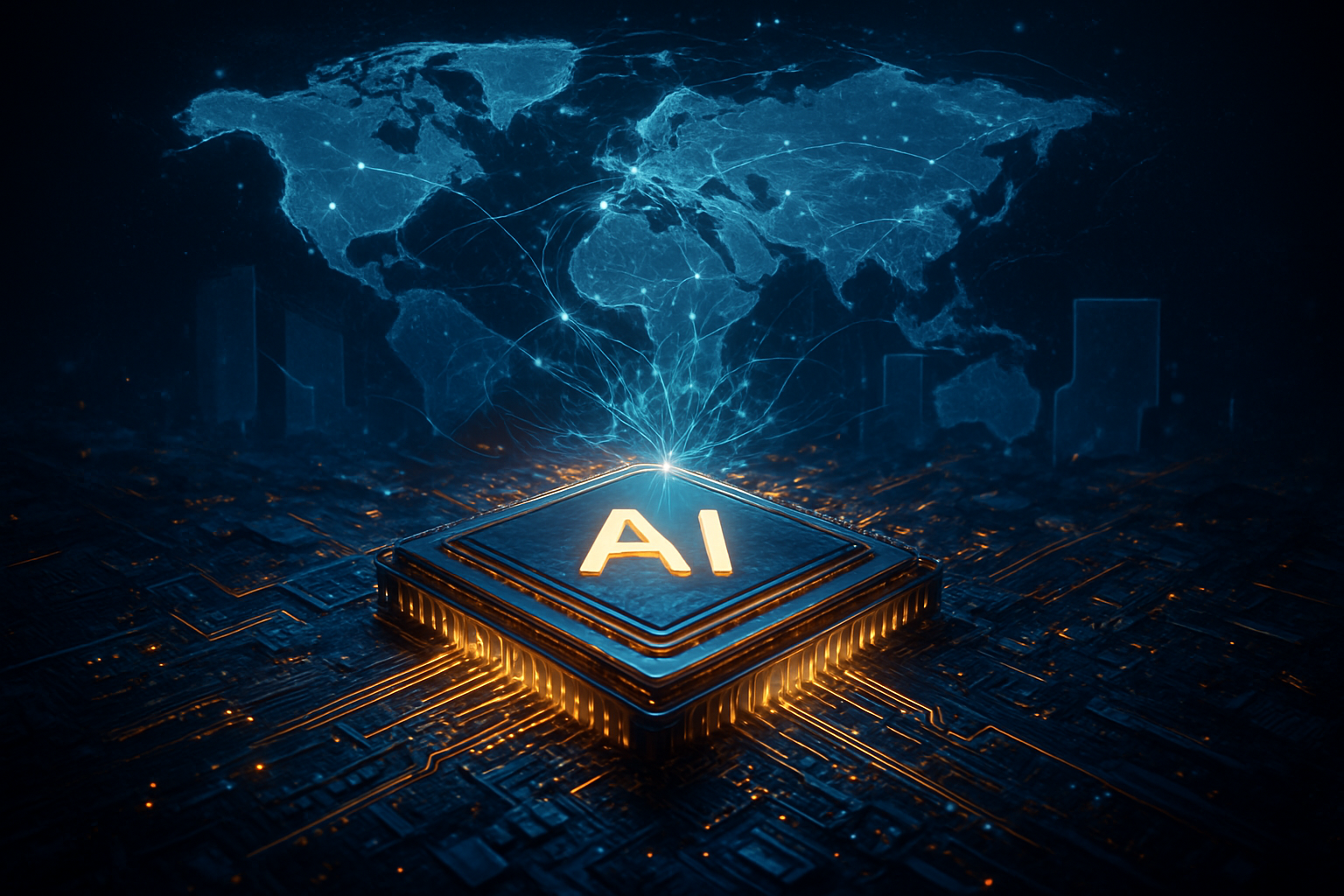
The long-promised era of "brain-like" computing has officially transitioned from academic curiosity to commercial reality. As of early 2026, a wave of breakthroughs in neuromorphic engineering is fundamentally reshaping how artificial intelligence interacts with the physical world. By mimicking the architecture of the human brain—where processing and memory are inextricably linked and neurons only fire when necessary—these new chips are enabling a generation of "always-on" devices that consume milliwatts of power while performing complex sensory tasks that previously required power-hungry GPUs.
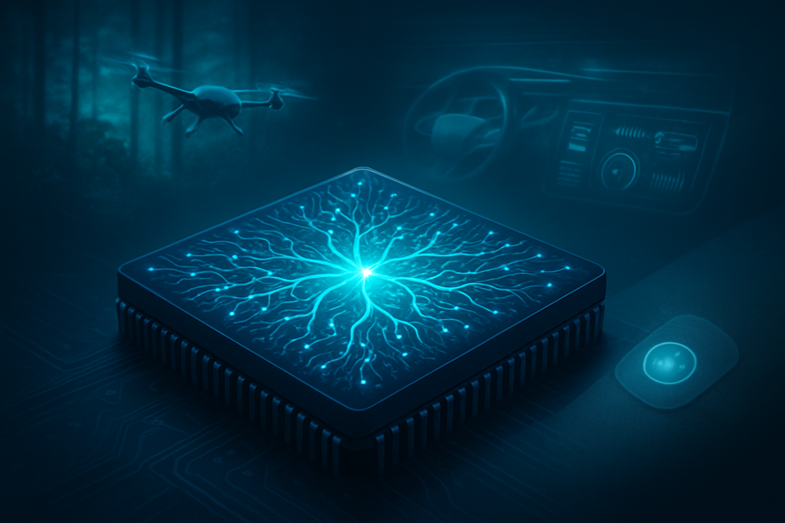
This shift marks the beginning of the end for the traditional von Neumann bottleneck, which has long separated processing and memory in standard computers. With the release of commercial-grade neuromorphic hardware this quarter, the industry is moving toward "Physical AI"—systems that can see, hear, and feel their environment in real-time with the energy efficiency of a biological organism. From autonomous drones that can navigate dense forests for hours on a single charge to wearable medical sensors that monitor heart health for years without a battery swap, neuromorphic computing is proving to be the missing link for the "trillion-sensor economy."
From Research to Real-Time: The Rise of Loihi 3 and NorthPole
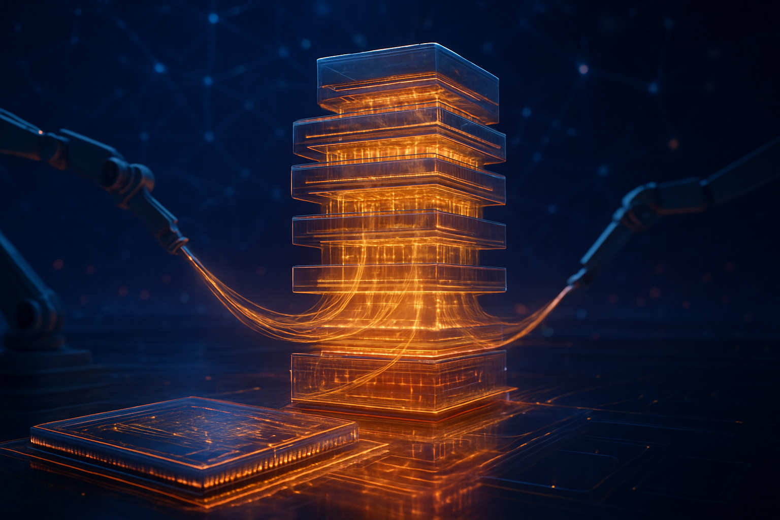
The technical landscape of early 2026 is dominated by the official release of Intel (NASDAQ:INTC) Loihi 3. Built on a cutting-edge 4nm process, Loihi 3 represents an 8x increase in density over its predecessor, packing 8 million neurons and 64 billion synapses into a single chip. Unlike traditional processors that constantly cycle through data, Loihi 3 utilizes asynchronous Spiking Neural Networks (SNNs), where information is processed as discrete "spikes" of activity. This allows the chip to consume a mere 1.2W at peak load—a staggering 250x reduction in energy compared to equivalent GPU-based inference for robotics and autonomous navigation.
Simultaneously, IBM (NYSE:IBM) has moved its "NorthPole" architecture into high-volume production. NorthPole differs from Intel’s approach by utilizing a "digital neuromorphic" design that eliminates external DRAM entirely, placing all memory directly on-chip to mimic the brain's localized processing. In recent benchmarks, NorthPole demonstrated 25x greater energy efficiency than the NVIDIA (NASDAQ:NVDA) H100 for vision-based tasks like ResNet-50. Perhaps more impressively, it has achieved sub-millisecond latency for 3-billion parameter Large Language Models (LLMs), enabling compact edge servers to perform complex reasoning without a cloud connection.
The third pillar of this technical revolution is "event-based" sensing. Traditional cameras capture 30 to 60 frames per second, processing every pixel regardless of whether it has changed. In contrast, neuromorphic vision sensors, such as those developed by Prophesee and integrated into SynSense’s Speck chip, only report changes in light at the individual pixel level. This reduces the data stream by up to 1,000x, allowing for millisecond-level reaction times in gesture control and obstacle avoidance while drawing less than 5 milliwatts of power.
The Business of Efficiency: Tech Giants vs. Neuromorphic Disruptors
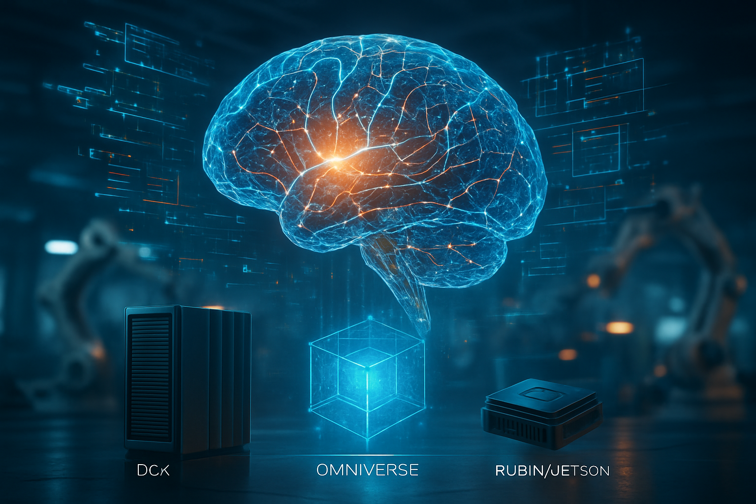
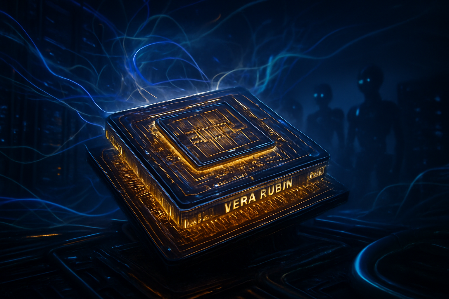
The commercialization of neuromorphic hardware has forced a strategic pivot among the world’s largest semiconductor firms. While NVIDIA (NASDAQ:NVDA) remains the undisputed king of the data center, it has responded to the neuromorphic threat by integrating "event-driven" sensor pipelines into its Blackwell and 2026-era "Vera Rubin" architectures. Through its Holoscan Sensor Bridge, NVIDIA is attempting to co-opt the low-latency advantages of neuromorphic systems by allowing sensors to stream data directly into GPU memory, bypassing traditional bottlenecks while still utilizing standard digital logic.
Arm (NASDAQ:ARM) has taken a different approach, embedding specialized "Neural Technology" directly into its GPU shaders for the 2026 mobile roadmap. By integrating mini-NPUs (Neural Processing Units) that handle sparse data-flow, Arm aims to maintain its dominance in the smartphone and wearable markets. However, specialized startups like BrainChip (ASX:BRN) and Innatera are successfully carving out a niche in the "extreme edge." BrainChip’s Akida 2.0 has already seen integration into production electric vehicles from Mercedes-Benz (OTC:MBGYY) for real-time driver monitoring, operating at a power draw of just 0.3W—a level traditional NPUs struggle to reach without significant thermal overhead.
This competition is creating a bifurcated market. High-performance "Physical AI" for humanoid robotics and autonomous vehicles is becoming a battleground between NVIDIA’s massive parallel processing and Intel’s neuromorphic efficiency. Meanwhile, the market for "always-on" consumer electronics—such as smart smoke detectors that can distinguish between a fire and a person, or AR glasses with 24-hour battery life—is increasingly dominated by neuromorphic IP that can operate in the microwatt range.
Beyond the Edge: Sustainability and the "Always-On" Society
The wider significance of these breakthroughs extends far beyond raw performance metrics; it is a critical component of the "Green AI" movement. As the energy demands of global AI infrastructure skyrocket, the ability to perform inference at 1/100th the power of a GPU is no longer just a cost-saving measure—it is a sustainability mandate. Neuromorphic chips allow for the deployment of sophisticated AI in environments where power is scarce, such as remote industrial sites, deep-sea exploration, and even long-term space missions.
Furthermore, the shift toward on-device neuromorphic processing offers a profound win for data privacy. Because these chips are efficient enough to process high-resolution sensory data locally, there is no longer a need to stream sensitive audio or video to the cloud for analysis. In 2026, "always-on" voice assistants and security cameras can operate entirely within the device's local "silicon brain," ensuring that personal data never leaves the premises. This "privacy-by-design" architecture is expected to accelerate the adoption of AI in healthcare and home automation, where consumer trust has previously been a barrier.
However, the transition is not without its challenges. The industry is currently grappling with the "software gap"—the difficulty of training traditional neural networks to run on spiking hardware. While the adoption of the NeuroBench framework in late 2025 has provided standardized metrics for efficiency, many developers still find the shift from frame-based to event-based programming to be a steep learning curve. The success of neuromorphic computing will ultimately depend on the maturity of these software ecosystems and the ability of tools like Intel’s Lava and BrainChip’s MetaTF to simplify SNN development.
The Horizon: Bio-Hybrids and the Future of Sensing
Looking ahead to the remainder of 2026 and 2027, experts predict the next frontier will be the integration of neuromorphic chips with biological interfaces. Research into "bio-hybrid" systems, where neuromorphic silicon is used to decode neural signals in real-time, is showing promise for a new generation of prosthetics that feel and move like natural limbs. These systems require the ultra-low latency and low power consumption that only neuromorphic architectures can provide to avoid the lag and heat generation of traditional processors.
In the near term, expect to see the "neuromorphic-first" approach dominate the drone industry. Companies are already testing "nano-drones" that weigh less than 30 grams but possess the visual intelligence of a predatory insect, capable of navigating complex indoor environments without human intervention. These use cases will likely expand into "smart city" infrastructure, where millions of tiny, battery-powered sensors will monitor everything from structural integrity to traffic flow, creating a self-aware urban environment that requires minimal maintenance.
A Tipping Point for Artificial Intelligence
The breakthroughs of early 2026 represent a fundamental shift in the AI trajectory. We are moving away from a world where AI is a distant, cloud-based brain and toward a world where intelligence is woven into the very fabric of our physical environment. Neuromorphic computing has proven that the path to more capable AI does not always require more power; sometimes, it simply requires a better blueprint—one that took nature millions of years to perfect.
As we look toward the coming months, the key indicators of success will be the volume of Loihi 3 deployments in industrial robotics and the speed at which "neuromorphic-inside" consumer products hit the shelves. The silicon brain has officially awakened, and its impact on the tech industry will be felt for decades to come.
This content is intended for informational purposes only and represents analysis of current AI developments.
TokenRing AI delivers enterprise-grade solutions for multi-agent AI workflow orchestration, AI-powered development tools, and seamless remote collaboration platforms.
For more information, visit https://www.tokenring.ai/.