As of early 2026, the global semiconductor industry has officially entered what analysts are calling the "Silicon Super-Cycle." Long characterized by its volatile boom-and-bust cycles, the sector has undergone a structural transformation, evolving from a provider of cyclical components into the foundational infrastructure of a new sovereign economy. Following a record-breaking 2025 that saw global revenues surge past $800 billion, consensus from major firms like McKinsey, Gartner, and IDC now confirms that the industry is on a definitive, accelerated path to exceed $1 trillion in annual revenue by 2030—with some aggressive forecasts suggesting the milestone could be reached as early as 2028.
The primary catalyst for this historic expansion is the insatiable demand for artificial intelligence, specifically the transition from simple generative chatbots to "Agentic AI" and "Physical AI." This shift has fundamentally rewired the global economy, turning compute capacity into a metric of national productivity. As the digital economy expands into every facet of industrial manufacturing, automotive transport, and healthcare, the semiconductor has become the "new oil," driving a massive wave of capital expenditure that is reshaping the geopolitical and corporate landscape of the 21st century.
The Angstrom Era: 2nm Nodes and the HBM4 Revolution
Technically, the road to $1 trillion is being paved with the most complex engineering feats in human history. As of January 2026, the industry has successfully transitioned into the "Angstrom Era," marked by the high-volume manufacturing of sub-2nm class chips. Taiwan Semiconductor Manufacturing Company (NYSE: TSM) began mass production of its 2nm (N2) node in late 2025, utilizing Nanosheet Gate-All-Around (GAA) transistors for the first time. This architecture replaces the decade-old FinFET design, allowing for a 30% reduction in power consumption—a critical requirement for the massive data centers powering today's trillion-parameter AI models. Meanwhile, Intel Corporation (NASDAQ: INTC) has made a significant comeback, reaching high-volume manufacturing on its 18A (1.8nm) node this week. Intel’s 18A is the first in the industry to combine GAA transistors with "PowerVia" backside power delivery, a technical leap that many experts believe could finally level the playing field with TSMC.
The hardware driving this revenue surge is no longer just about the logic processor; it is about the "memory wall." The debut of the HBM4 (High-Bandwidth Memory) standard in early 2026 has doubled the interface width to 2048-bit, providing the massive data throughput required for real-time AI reasoning. To house these components, advanced packaging techniques like CoWoS-L and the emergence of glass substrates have become the new industry bottlenecks. Companies are no longer just "printing" chips; they are building 3D-stacked "superchips" that integrate logic, memory, and optical interconnects into a single, highly efficient package.
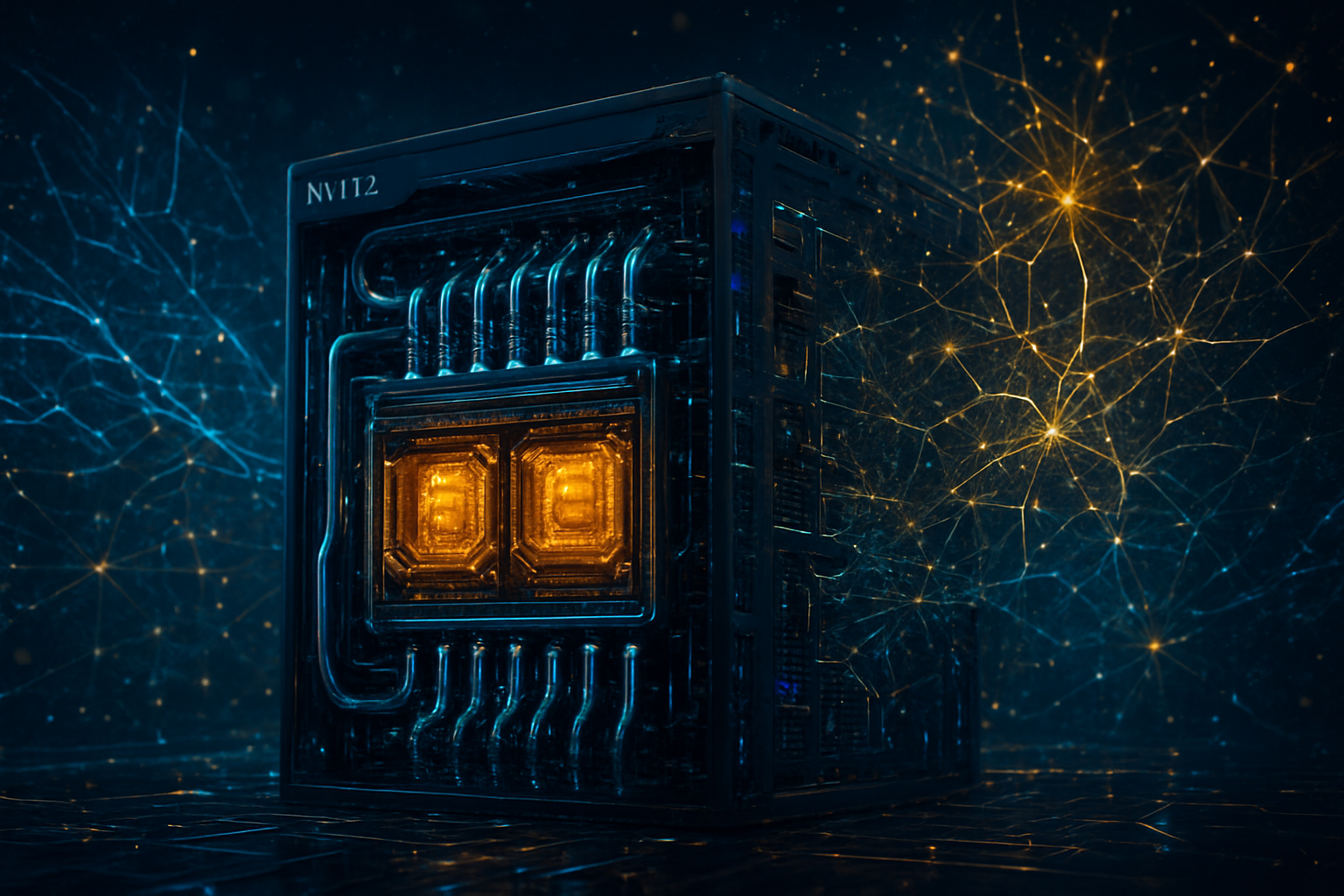
Initial reactions from the AI research community have been electric, particularly following the unveiling of the Vera Rubin architecture by NVIDIA (NASDAQ: NVDA) at CES 2026. The Rubin GPU, built on TSMC’s N3P process and utilizing HBM4, offers a 2.5x performance increase over the previous Blackwell generation. This relentless annual release cadence from chipmakers has forced AI labs to accelerate their own development cycles, as the hardware now enables the training of models that were computationally impossible just 24 months ago.
The Trillion-Dollar Corporate Landscape: Merchants vs. Hyperscalers
The race to $1 trillion has created a new class of corporate titans. NVIDIA continues to dominate the headlines, with its market capitalization hovering near the $5 trillion mark as of January 2026. By shifting to a strict one-year product cycle, NVIDIA has maintained a "moat of velocity" that competitors struggle to bridge. However, the competitive landscape is shifting as the "Magnificent Seven" move from being NVIDIA’s best customers to its most formidable rivals. Amazon (NASDAQ: AMZN), Google (NASDAQ: GOOGL), Microsoft (NASDAQ: MSFT), and Meta (NASDAQ: META) have all successfully productionized their own custom AI silicon—such as Amazon’s Trainium 3 and Google’s TPU v7.
These custom ASICs (Application-Specific Integrated Circuits) are increasingly winning the battle for "Inference"—the process of running AI models—where power efficiency and cost-per-token are more important than raw flexibility. While NVIDIA remains the undisputed king of frontier model training, the rise of custom silicon allows hyperscalers to bypass the "NVIDIA tax" for their internal workloads. This has forced Advanced Micro Devices (NASDAQ: AMD) to pivot its strategy toward being the "open alternative," with its Instinct MI400 series capturing a significant 30% share of the data center GPU market by offering massive memory capacities that appeal to open-source developers.
Furthermore, a new trend of "Sovereign AI" has emerged as a major revenue driver. Nations such as Saudi Arabia, the UAE, Japan, and France are now treating compute capacity as a strategic national reserve. Through initiatives like Saudi Arabia's ALAT and Japan’s Rapidus project, governments are spending tens of billions of dollars to build domestic AI clusters and fabrication plants. This "nationalization" of compute ensures that the demand for high-end silicon remains decoupled from traditional consumer spending cycles, providing a stable floor for the industry's $1 trillion ambitions.
Geopolitics, Energy, and the "Silicon Sovereignty" Trend
The wider significance of the semiconductor's path to $1 trillion extends far beyond balance sheets; it is now the central pillar of global geopolitics. The "Chip War" between the U.S. and China has reached a protracted stalemate in early 2026. While the U.S. has tightened export controls on ASML (NASDAQ: ASML) High-NA EUV lithography machines, China has retaliated with strict export curbs on the rare-earth elements essential for chip manufacturing. This friction has accelerated the "de-risking" of supply chains, with the U.S. CHIPS Act 2.0 providing even deeper subsidies to ensure that 20% of the world’s most advanced logic chips are produced on American soil by 2030.
However, this explosive growth has hit a physical wall: energy. AI data centers are projected to consume up to 12% of total U.S. electricity by 2030. To combat this, the industry is leading a "Nuclear Renaissance." Hyperscalers are no longer just buying green energy credits; they are directly investing in Small Modular Reactors (SMRs) to provide dedicated, carbon-free baseload power to their AI campuses. The environmental impact is also under scrutiny, as the manufacturing of 2nm chips requires astronomical amounts of ultrapure water. In response, leaders like Intel and TSMC have committed to "Net Positive Water" goals, implementing 98% recycling rates to mitigate the strain on local resources.
This era is often compared to the Industrial Revolution or the dawn of the Internet, but the speed of the "Silicon Renaissance" is unprecedented. Unlike the PC or smartphone eras, which took decades to mature, the AI-driven demand for semiconductors is scaling exponentially. The industry is no longer just supporting the digital economy; it is the digital economy. The primary concern among experts is no longer a lack of demand, but a lack of talent—with a projected global shortage of one million skilled workers needed to staff the 70+ new "mega-fabs" currently under construction worldwide.
Future Horizons: 1nm Nodes and Silicon Photonics
Looking toward the end of the decade, the roadmap for the semiconductor industry remains aggressive. By 2028, the industry expects to debut the 1nm (A10) node, which will likely utilize Complementary FET (CFET) architectures—stacking transistors vertically to double density without increasing the chip's footprint. Beyond 1nm, researchers are exploring exotic 2D materials like molybdenum disulfide to overcome the quantum tunneling effects that plague silicon at atomic scales.
Perhaps the most significant shift on the horizon is the transition to Silicon Photonics. As copper wires reach their physical limits for data transfer, the industry is moving toward light-based computing. By 2030, optical I/O will likely be the standard for chip-to-chip communication, drastically reducing the energy "tax" of moving data. Experts predict that by 2032, we will see the first hybrid electron-light processors, which could offer another 10x leap in AI efficiency, potentially pushing the industry toward a $2 trillion milestone by the 2040s.
The Inevitable Ascent: A Summary of the $1 Trillion Path
The semiconductor industry’s journey to $1 trillion by 2030 is more than just a financial forecast; it is a testament to the essential nature of compute in the modern world. The key takeaways for 2026 are clear: the transition to 2nm and 18A nodes is successful, the "Memory Wall" is being breached by HBM4, and the rise of custom and sovereign silicon has diversified the market beyond traditional PC and smartphone chips. While energy constraints and geopolitical tensions remain significant headwinds, the sheer momentum of AI integration into the global economy appears unstoppable.
This development marks a definitive turning point in technology history—the moment when silicon became the most valuable commodity on Earth. In the coming months, investors and industry watchers should keep a close eye on the yield rates of Intel’s 18A node and the rollout of NVIDIA’s Rubin platform. As the industry scales toward the $1 trillion mark, the companies that can solve the triple-threat of power, heat, and talent will be the ones that define the next decade of human progress.
This content is intended for informational purposes only and represents analysis of current AI developments.
TokenRing AI delivers enterprise-grade solutions for multi-agent AI workflow orchestration, AI-powered development tools, and seamless remote collaboration platforms.
For more information, visit https://www.tokenring.ai/.