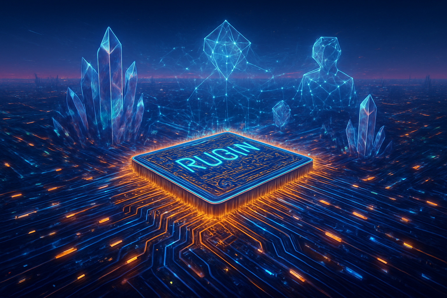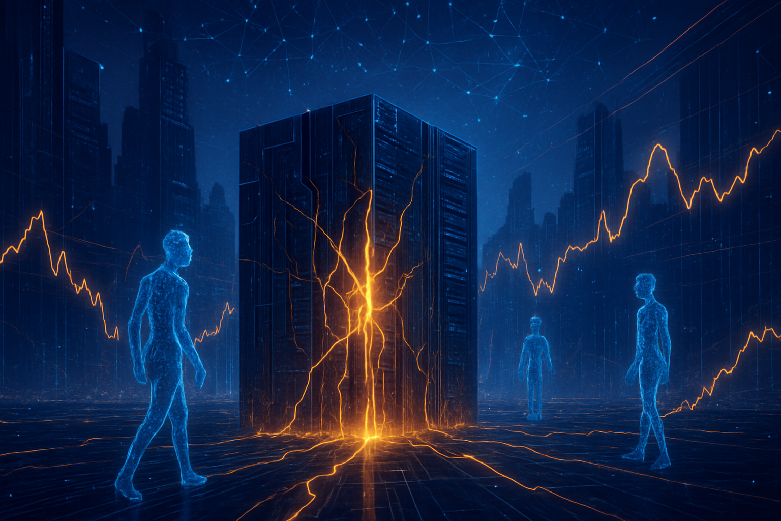
As of early 2026, the global artificial intelligence landscape has fractured into two distinct hemispheres. While the West continues to push the boundaries of single-chip efficiency with Blackwell and Rubin architectures from NVIDIA (NASDAQ: NVDA), China has rapidly consolidated its digital future around a domestic champion: Huawei. Once a secondary alternative to Western hardware, Huawei’s Ascend AI ecosystem has now become the primary pillar of China’s computational infrastructure, scaling up with unprecedented speed to mitigate the impact of tightening US export controls.
This shift marks a critical turning point in the global tech war. With the recent launch of the Ascend 950PR and the widespread deployment of the Ascend 910C, Huawei is no longer just selling chips; it is providing a full-stack, "sovereign AI" solution that includes silicon, specialized software, and massive-scale clustering technology. This domestic scaling is not merely a response to necessity—it is a strategic re-engineering of how AI is trained and deployed in the world’s second-largest economy.
The Hardware of Sovereignty: Inside the Ascend 910C and 950PR
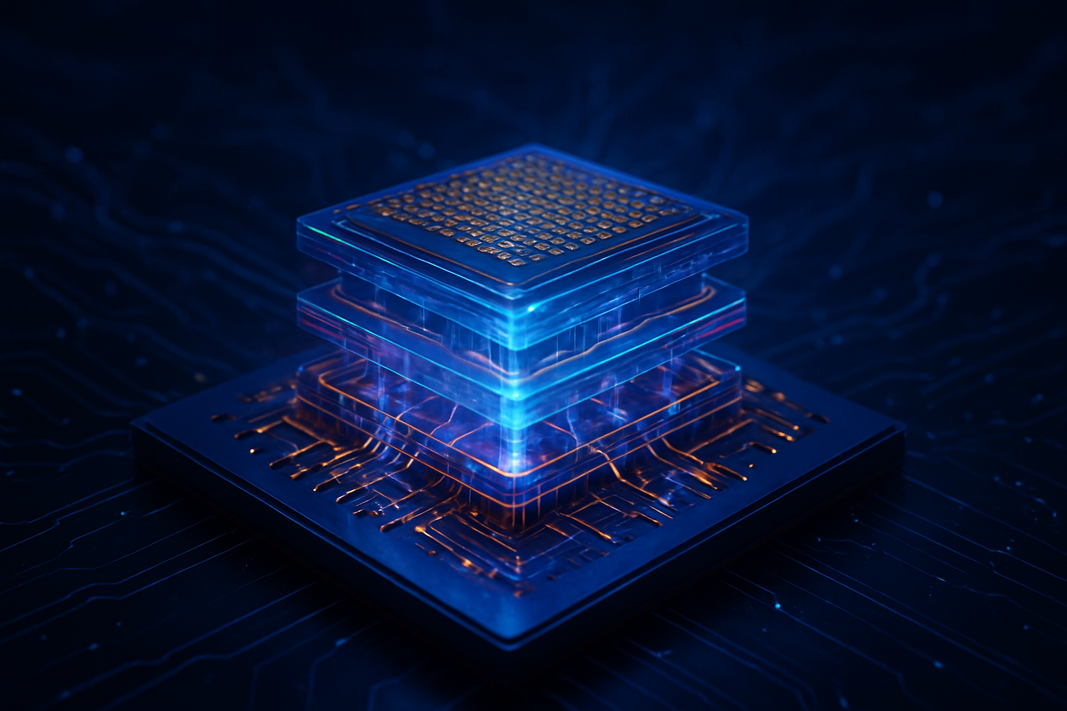
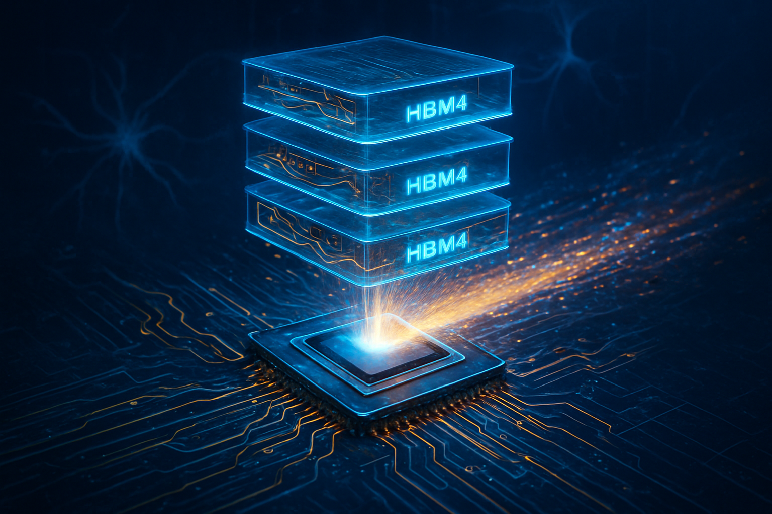
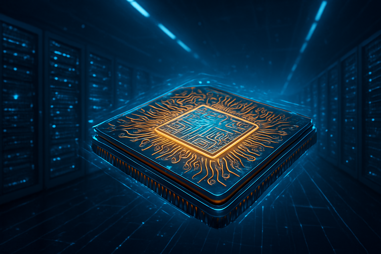
At the heart of Huawei’s 2026 strategy is the Ascend 910C, a "workhorse" chip that has achieved nearly 80% of the raw compute performance of NVIDIA’s H100. Despite being manufactured on SMIC (HKG: 0981) 7nm (N+2) nodes—which lack the efficiency of the 4nm processes used by Western rivals—the 910C utilizes a sophisticated dual-chiplet design to maximize throughput. To further close the gap, Huawei recently introduced the Ascend 950PR in Q1 2026. This new chip targets high-throughput inference and features Huawei’s first proprietary high-bandwidth memory, known as HiBL 1.0, developed in collaboration with domestic memory giant CXMT.
The technical specifications of the Ascend 950PR reflect a shift toward specialized AI tasks. While it trails NVIDIA’s B200 in raw FP16 performance, the 950PR is optimized for "Prefill and Recommendation" tasks, boasting a unified interconnect (UnifiedBus 2.0) that allows for the seamless clustering of up to one million NPUs. This "brute force" scaling strategy—connecting thousands of less-efficient chips into a single "SuperCluster"—allows Chinese firms to achieve the same total FLOPs as Western data centers, albeit at a higher power cost.
Industry experts have noted that the software layer, once Huawei’s greatest weakness, has matured significantly. The Compute Architecture for Neural Networks (CANN) 8.0/9.0 has become a viable alternative to NVIDIA’s CUDA. In late 2025, Huawei’s decision to open-source CANN triggered a massive influx of domestic developers who have since optimized kernels for major models like Llama-3 and Qwen. The introduction of automated "CUDA-to-CANN" conversion tools has lowered the migration barrier, making it easier for Chinese researchers to port their existing workloads to Ascend hardware.
A New Market Order: The Flight to Domestic Silicon
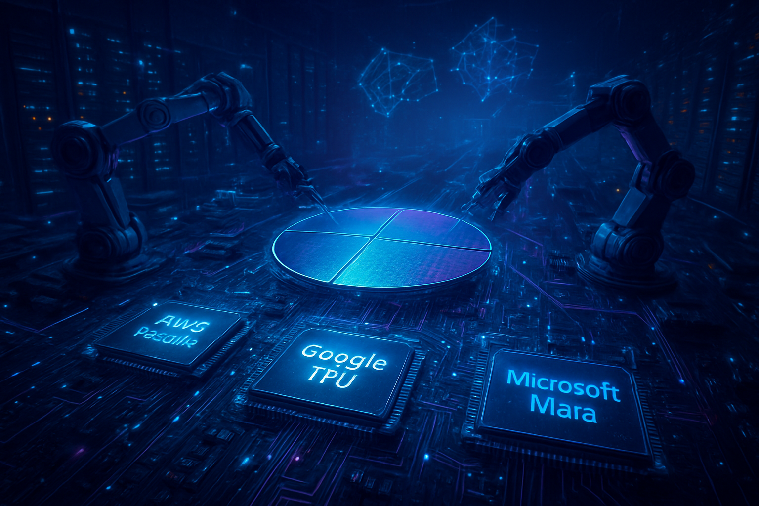
The competitive landscape for AI chips in China has undergone a radical transformation. Major tech giants that once relied on "China-compliant" (H20/H800) chips from NVIDIA or AMD (NASDAQ: AMD) are now placing multi-billion dollar orders with Huawei. ByteDance, the parent company of TikTok, reportedly finalized a $5.6 billion order for Ascend chips for the 2026-2027 cycle, signaling a definitive move away from foreign dependencies. This shift is driven by the increasing unreliability of US supply chains and the superior vertical integration offered by the Huawei-Baidu (NASDAQ: BIDU) alliance.
Baidu and Huawei now control nearly 70% of China’s GPU cloud market. By deeply integrating Baidu’s PaddlePaddle framework with Huawei’s hardware, the duo has created an optimized stack that rivals the performance of the NVIDIA-PyTorch ecosystem. Other giants like Alibaba (NYSE: BABA) and Tencent (HKG: 0700), while still developing their own internal AI chips, have deployed massive "CloudMatrix 384" clusters—Huawei’s domestic equivalent to NVIDIA’s GB200 NVL72 racks—to power their latest generative AI services.
This mass adoption has created a "virtuous cycle" for Huawei. As more companies migrate to Ascend, the software ecosystem improves, which in turn attracts more users. This has placed significant pressure on NVIDIA’s remaining market share in China. While NVIDIA still holds a technical lead, the geopolitical risk associated with its hardware has made it a "legacy" choice for state-backed enterprises and major internet firms alike, effectively creating a closed-loop market where Huawei is the undisputed leader.
The Geopolitical Divide and the "East-to-West" Strategy
The rise of the Ascend ecosystem is more than a corporate success story; it is a manifestation of China’s "Self-Reliance" mandate. As the US-led "Pax Silica" coalition tightens restrictions on advanced lithography and high-bandwidth memory from SK Hynix (KRX: 000660) and Samsung (KRX: 0005930), China has leaned into its "Eastern Data, Western Computing" project. This initiative leverages the abundance of subsidized green energy in western provinces like Ningxia and Inner Mongolia to power the massive, energy-intensive Ascend clusters required to match Western AI capabilities.
This development mirrors previous technological milestones, such as the emergence of the 5G standard, where a clear divide formed between Chinese and Western technical stacks. However, the stakes in AI are significantly higher. By building a parallel AI infrastructure, China is ensuring that its "Intelligence Economy" remains insulated from external sanctions. The success of domestic models like DeepSeek-R1, which was partially trained on Ascend hardware, has proven that algorithmic efficiency can, to some extent, compensate for the hardware performance gap.
However, concerns remain regarding the sustainability of this "brute force" approach. The reliance on multi-patterning lithography and lower-yield 7nm/5nm nodes makes the production of Ascend chips significantly more expensive than their Western counterparts. While the Chinese government provides massive subsidies to bridge this gap, the long-term economic viability depends on whether Huawei can continue to innovate in chiplet design and 3D packaging to overcome the lack of Extreme Ultraviolet (EUV) lithography.
Looking Ahead: The Road to 5nm and Beyond
The near-term roadmap for Huawei focuses on the Ascend 950DT, expected in late 2026. This "Decoding and Training" variant is designed to compete directly with Blackwell-level systems by utilizing HiZQ 2.0 HBM, which aims for a 4 TB/s bandwidth. If successful, this would represent the most significant leap in Chinese domestic chip performance to date, potentially bringing the performance gap with NVIDIA down to less than a single generation.
Challenges remain, particularly in the mass production of domestic HBM. While the CXMT-led consortium has made strides, their current HBM3-class memory is still one to two generations behind the HBM3e and HBM4 standards being pioneered by SK Hynix. Furthermore, the yield rates at SMIC’s advanced nodes remain a closely guarded secret, with some analysts estimating them as low as 40%. Improving these yields will be critical for Huawei to meet the soaring demand from the domestic market.
Experts predict that the next two years will see a "software-first" revolution in China. With hardware scaling hitting physical limits due to sanctions, the focus will shift toward specialized AI compilers and sparse-computation algorithms that extract every ounce of performance from the Ascend architecture. If Huawei can maintain its current trajectory, it may not only secure the Chinese market but also begin exporting its "AI-in-a-box" solutions to other nations seeking digital sovereignty from the US tech sphere.
Summary: A Bifurcated AI Future
The scaling of the Huawei Ascend ecosystem is a landmark event in the history of artificial intelligence. It represents the first time a domestic challenger has successfully built a comprehensive alternative to the dominant Western AI stack under extreme adversarial conditions. Key takeaways include the maturation of the CANN software ecosystem, the "brute force" success of large-scale clusters, and the definitive shift of Chinese tech giants toward local silicon.
As we move further into 2026, the global tech industry must grapple with a bifurcated reality. The era of a single, unified AI development path is over. In its place are two competing ecosystems, each with its own hardware standards, software frameworks, and strategic philosophies. For the coming months, the industry should watch closely for the first benchmarks of the Ascend 950DT and any further developments in China’s domestic HBM production, as these will determine just how high Huawei’s silicon shield can rise.
This content is intended for informational purposes only and represents analysis of current AI developments.
TokenRing AI delivers enterprise-grade solutions for multi-agent AI workflow orchestration, AI-powered development tools, and seamless remote collaboration platforms.
For more information, visit https://www.tokenring.ai/.