In a landmark achievement for computational medicine, researchers at Harvard Medical School have developed a "generalist" artificial intelligence model that is fundamentally reshaping the landscape of oncology. Known as the Clinical Histopathology Imaging Evaluation Foundation (CHIEF), this AI system has demonstrated a staggering 98% accuracy in diagnosing rare and metastatic cancers, while simultaneously predicting patient survival rates across 19 different anatomical sites. Unlike the "narrow" AI tools of the past, CHIEF operates as a foundation model, often referred to by the research community as the "ChatGPT of cancer diagnosis."
The immediate significance of CHIEF lies in its versatility and its ability to see what the human eye cannot. By analyzing standard pathology slides, the model can identify tumor cells, predict molecular mutations, and forecast long-term clinical outcomes with a level of precision that was previously unattainable. As of early 2026, CHIEF has moved from a theoretical breakthrough published in Nature to a cornerstone of digital pathology, offering a standardized, high-performance diagnostic layer that can be deployed across diverse clinical settings globally.
The Technical Core: Beyond Narrow AI
Technically, CHIEF represents a departure from traditional supervised learning models that require thousands of manually labeled images. Instead, the Harvard team utilized a self-supervised learning approach, pre-training the model on a massive dataset of 15 million unlabeled image patches. This was followed by a refinement process using 60,530 whole-slide images (WSIs) spanning 19 different organ systems, including the lung, breast, prostate, and brain. By ingesting approximately 44 terabytes of high-resolution data, CHIEF learned the "geometry and grammar" of human tissue, allowing it to generalize its knowledge across different types of cancer without needing specific re-training for each organ.
The performance metrics of CHIEF are unparalleled. In validation tests involving over 19,400 slides from 24 hospitals worldwide, the model achieved nearly 94% accuracy in general cancer detection. However, its most impressive feat is its 98% accuracy rate in identifying rare and metastatic cancers—areas where even experienced pathologists often face significant challenges. Furthermore, CHIEF can predict genetic mutations directly from a standard microscope slide, such as the EZH2 mutation in lymphoma (96% accuracy) and BRAF in thyroid cancer (89% accuracy), effectively bypassing the need for expensive and time-consuming genomic sequencing in many cases.
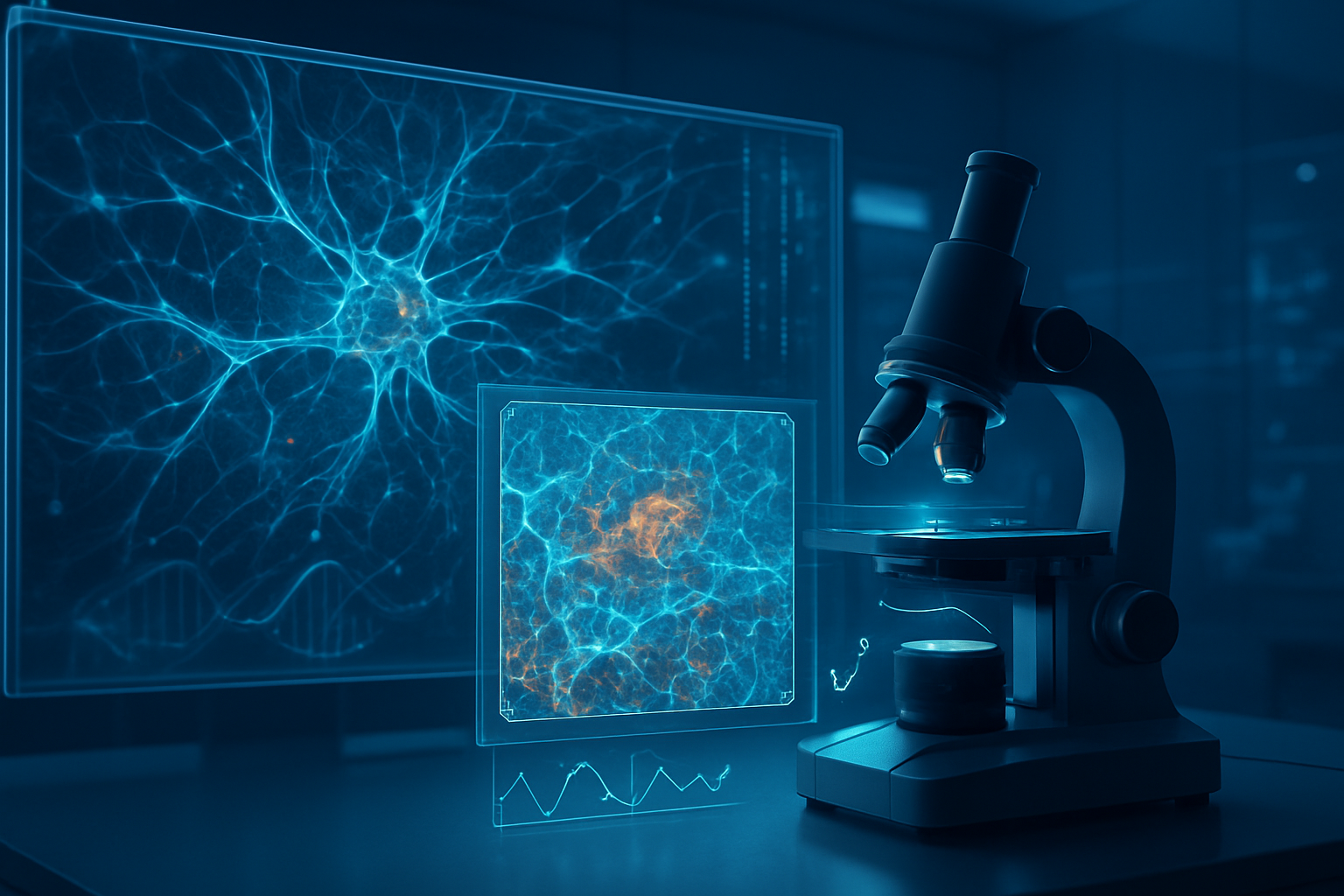
Beyond simple detection, CHIEF excels at prognosis. By analyzing the "tumor microenvironment"—the complex interplay between immune cells, blood vessels, and connective tissue—the model can distinguish between patients with long-term and short-term survival prospects with an accuracy 8% to 10% higher than previous state-of-the-art AI systems. It generates heat maps that visualize "hot spots" of tumor aggressiveness, providing clinicians with a visual roadmap of a patient's specific cancer profile.
The AI research community has hailed CHIEF as a "Swiss Army Knife" for pathology. Experts note that while previous models were "narrow"—meaning a model trained for lung cancer could not be used for breast cancer—CHIEF’s foundation model architecture allows it to be "plug-and-play." This robustness ensures that the model maintains its accuracy even when analyzing slides prepared with different staining techniques or digitized by different scanners, a hurdle that has historically limited the clinical adoption of medical AI.
Market Disruption and Corporate Strategic Shifts
The rise of foundation models like CHIEF is creating a seismic shift for major technology and healthcare companies. NVIDIA (NASDAQ:NVDA) stands as a primary beneficiary, as the massive computational power required to train and run CHIEF-scale models has cemented the company’s H100 and B200 GPU architectures as the essential infrastructure for the next generation of medical AI. NVIDIA has increasingly positioned healthcare as its most lucrative "generative AI" vertical, using breakthroughs like CHIEF to forge deeper ties with hospital networks and diagnostic manufacturers.
For traditional diagnostic giants like Roche (OTC:RHHBY), CHIEF presents a complex "threat and opportunity" dynamic. Roche’s core business includes the sale of molecular sequencing kits and diagnostic assays. CHIEF’s ability to predict genetic mutations directly from a $20 pathology slide could potentially disrupt the market for $3,000 genomic tests. To counter this, Roche has actively collaborated with academic institutions to integrate foundation models into their own digital pathology workflows, aiming to remain the "operating system" for the modern lab.
Similarly, GE Healthcare (NASDAQ:GEHC) and Johnson & Johnson (NYSE:JNJ) are racing to integrate CHIEF-like capabilities into their imaging and surgical platforms. GE Healthcare has been particularly aggressive in its vision of a "digital pathology app store," where CHIEF could serve as a foundational layer upon which other specialized diagnostic tools are built. This consolidation of AI tools into a single, generalist model reduces the "vendor fatigue" felt by hospitals, which previously had to manage dozens of siloed AI applications for different diseases.
The competitive landscape is also shifting for AI startups. While the "narrow AI" startups of the early 2020s are struggling to compete with the breadth of CHIEF, new ventures are emerging that focus on "fine-tuning" Harvard’s open-source architecture for specific clinical trials or ultra-rare diseases. This democratization of high-end AI allows smaller institutions to leverage expert-level diagnostic power without the billion-dollar R&D budgets of Big Tech.
Wider Significance: The Dawn of Generalist Medical AI
In the broader AI landscape, CHIEF marks the arrival of Generalist Medical AI (GMAI). This trend mirrors the evolution of Large Language Models (LLMs) like GPT-4, which moved away from task-specific programming toward broad, multi-purpose intelligence. CHIEF’s success proves that the "foundation model" approach is not just for text and images but is deeply applicable to the biological complexities of human disease. This shift is expected to accelerate the move toward "precision medicine," where treatment is tailored to the specific biological signature of an individual’s tumor.
However, the widespread adoption of such a powerful tool brings significant concerns. The "black box" nature of AI remains a point of contention; while CHIEF provides heat maps to explain its reasoning, the underlying neural pathways that lead to a 98% accuracy rating are not always fully transparent to human clinicians. There are also valid concerns regarding health equity. If CHIEF is trained primarily on datasets from Western hospitals, its performance on diverse global populations must be rigorously validated to ensure that its "98% accuracy" holds true for all patients, regardless of ethnicity or geographic location.
Comparatively, CHIEF is being viewed as the "AlphaFold moment" for pathology. Just as Google DeepMind’s AlphaFold solved the protein-folding problem, CHIEF is seen as solving the "generalization problem" in digital pathology. It has moved the conversation from "Can AI help a pathologist?" to "How can we safely integrate this AI as the primary diagnostic screening layer?" This transition marks a fundamental change in the role of the pathologist, who is evolving from a manual observer to a high-level data interpreter.
Future Horizons: Clinical Trials and Drug Discovery
Looking ahead, the near-term focus for CHIEF and its successors will be regulatory approval and clinical integration. While the model has been validated on retrospective data, prospective clinical trials are currently underway to determine how its use affects patient outcomes in real-time. Experts predict that within the next 24 months, we will see the first FDA-cleared "generalist" pathology models that can be used for primary diagnosis across multiple cancer types simultaneously.
The potential applications for CHIEF extend beyond the hospital walls. In the pharmaceutical industry, companies like Illumina (NASDAQ:ILMN) and others are exploring how CHIEF can be used to identify patients who are most likely to respond to specific immunotherapies. By identifying subtle morphological patterns in tumor slides, CHIEF could act as a powerful "biomarker discovery engine," significantly reducing the cost and failure rate of clinical trials for new cancer drugs.
Challenges remain, particularly in the realm of data privacy and the "edge" deployment of these models. Running a 44-terabyte-trained model requires significant local compute or secure cloud access, which may be a barrier for rural or under-resourced clinics. Addressing these infrastructure gaps will be the next major hurdle for the tech industry as it seeks to scale Harvard’s breakthrough to the global population.
Final Assessment: A Pillar of Modern Oncology
Harvard’s CHIEF AI stands as a definitive milestone in the history of medical technology. By achieving 98% accuracy in rare cancer diagnosis and providing superior survival predictions across 19 cancer types, it has proven that foundation models are the future of clinical diagnostics. The transition from narrow, organ-specific AI to generalist systems like CHIEF marks the beginning of a new era in oncology—one where "invisible" biological signals are transformed into actionable clinical insights.
As we move through 2026, the tech industry and the medical community will be watching closely to see how these models are governed and integrated into the standard of care. The key takeaways are clear: AI is no longer just a supportive tool; it is becoming the primary engine of diagnostic precision. For patients, this means faster diagnoses, more accurate prognoses, and treatments that are more closely aligned with their unique biological reality.
This content is intended for informational purposes only and represents analysis of current AI developments.
TokenRing AI delivers enterprise-grade solutions for multi-agent AI workflow orchestration, AI-powered development tools, and seamless remote collaboration platforms.
For more information, visit https://www.tokenring.ai/.