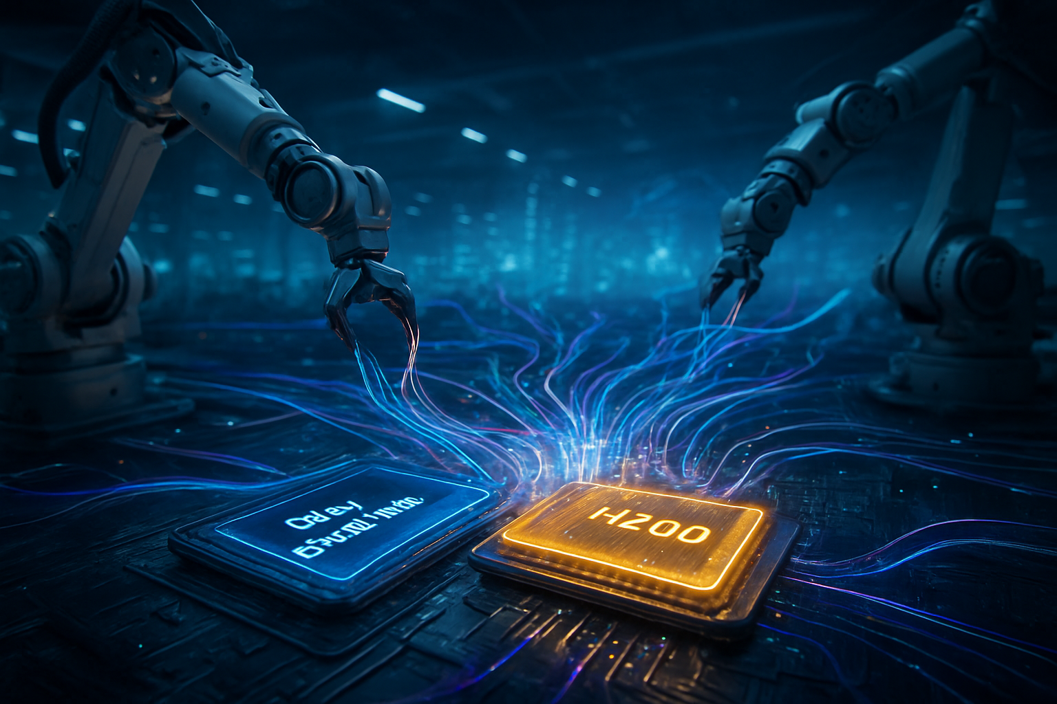
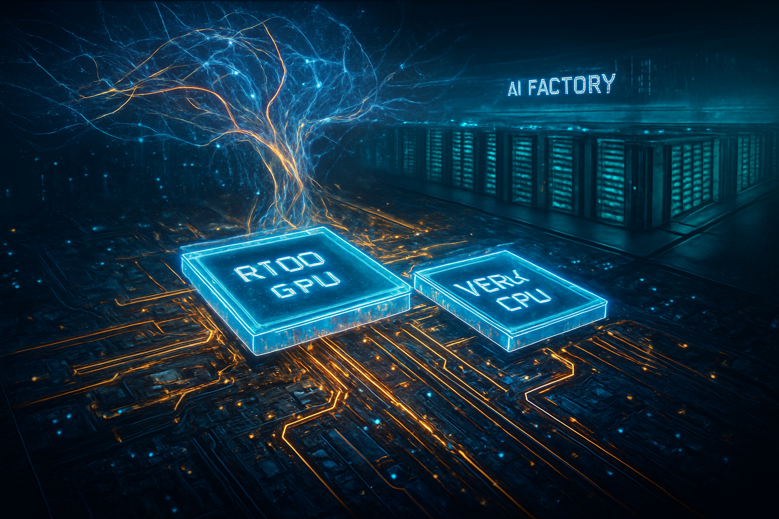
Tag: Nvidia

  • Nvidia’s $20 Billion Strategic Gambit: Acquihiring Groq to Define the Era of Real-Time Inference

    Nvidia’s $20 Billion Strategic Gambit: Acquihiring Groq to Define the Era of Real-Time Inference

    In a move that has sent shockwaves through the semiconductor industry, NVIDIA (NASDAQ: NVDA) has finalized a landmark $20 billion "license-and-acquihire" deal with the high-speed AI chip startup Groq. Announced in late December 2025, the transaction represents Nvidia’s largest strategic maneuver since its failed bid for Arm, signaling a definitive shift in the company’s focus from the heavy lifting of AI training to the lightning-fast world of real-time AI inference. By absorbing the leadership and core intellectual property of the company that pioneered the Language Processing Unit (LPU), Nvidia is positioning itself to own the entire lifecycle of the "AI Factory."

    The deal is structured to navigate an increasingly complex regulatory landscape, utilizing a "reverse acqui-hire" model that brings Groq’s visionary founders, Jonathan Ross and Sunny Madra, directly into Nvidia’s executive ranks while securing long-term licensing for Groq’s deterministic hardware architecture. As the industry moves away from static chatbots and toward "agentic AI"—autonomous systems that must reason and act in milliseconds—Nvidia’s integration of LPU technology effectively closes the performance gap that specialized ASICs (Application-Specific Integrated Circuits) had begun to exploit.

    The LPU Integration: Solving the "Memory Wall" for the Vera Rubin Era

    At the heart of this $20 billion deal is Groq’s proprietary LPU technology, which Nvidia plans to integrate into its upcoming "Vera Rubin" architecture, slated for a 2026 rollout. Unlike traditional GPUs that rely heavily on High Bandwidth Memory (HBM)—a component that has faced persistent supply shortages and high power costs—Groq’s LPU utilizes on-chip SRAM. This technical pivot allows for "Batch Size 1" processing, enabling the generation of thousands of tokens per second for a single user without the latency penalties associated with data movement in traditional architectures.

    Industry experts note that this integration addresses the "Memory Wall," a long-standing bottleneck where processor speeds outpace the ability of memory to deliver data. By incorporating Groq’s deterministic software stack, which predicts exact execution times for AI workloads, Nvidia’s next-generation "AI Factories" will be able to offer unprecedented reliability for mission-critical applications. Initial benchmarks suggest that LPU-enhanced Nvidia systems could be up to 10 times more energy-efficient per token than current H100 or B200 configurations, a critical factor as global data center power consumption reaches a tipping point.

    Strengthening the Moat: Competitive Fallout and Market Realignment

    The move is a strategic masterstroke that complicates the roadmap for Nvidia’s primary rivals, including Advanced Micro Devices (NASDAQ: AMD) and Intel (NASDAQ: INTC), as well as cloud-native chip efforts from Alphabet (NASDAQ: GOOGL) and Amazon (NASDAQ: AMZN). By bringing Jonathan Ross—the original architect of Google’s TPU—into the fold as Nvidia’s new Chief Software Architect, CEO Jensen Huang has effectively neutralized one of his most formidable intellectual competitors. Sunny Madra, who joins as VP of Hardware, is expected to spearhead the effort to make LPU technology "invisible" to developers by absorbing it into the existing CUDA ecosystem.

    For the broader startup ecosystem, the deal is a double-edged sword. While it validates the massive valuations of specialized AI silicon companies, it also demonstrates Nvidia’s willingness to spend aggressively to maintain its ~90% market share. Startups focusing on inference-only hardware now face a competitor that possesses both the industry-standard software stack and the most advanced low-latency hardware IP. Analysts suggest that this "license-and-acquihire" structure may become the new blueprint for Big Tech acquisitions, allowing giants to bypass traditional antitrust blocks while still securing the talent and tech they need to stay ahead.

    Beyond GPUs: The Rise of the Hybrid AI Factory

    The significance of this deal extends far beyond a simple hardware upgrade; it represents the maturation of the AI landscape. In 2023 and 2024, the industry was obsessed with training larger and more capable models. By late 2025, the focus has shifted entirely to inference—the actual deployment and usage of these models in the real world. Nvidia’s "AI Factory" vision now includes a hybrid silicon approach: GPUs for massive parallel training and LPU-derived cores for instantaneous, agentic reasoning.

    This shift mirrors previous milestones in computing history, such as the transition from general-purpose CPUs to specialized graphics accelerators in the 1990s. By internalizing the LPU, Nvidia is acknowledging that the "one-size-fits-all" GPU era is evolving. There are, however, concerns regarding market consolidation. With Nvidia controlling both the training and the most efficient inference hardware, the "CUDA Moat" has become more of a "CUDA Fortress," raising questions about long-term pricing power and the ability of smaller players to compete without Nvidia’s blessing.

    The Road to 2026: Agentic AI and Autonomous Systems

    Looking ahead, the immediate priority for the newly combined teams will be the release of updated TensorRT and Triton libraries. These software updates are expected to allow existing AI models to run on LPU-enhanced hardware with zero code changes, a move that would facilitate an overnight performance boost for thousands of enterprise customers. Near-term applications are likely to focus on voice-to-voice translation, real-time financial trading algorithms, and autonomous robotics, all of which require the sub-100ms response times that the Groq-Nvidia hybrid architecture promises.

    However, challenges remain. Integrating two radically different hardware philosophies—the stochastic nature of traditional GPUs and the deterministic nature of LPUs—will require a massive engineering effort. Experts predict that the first "true" hybrid chip will not hit the market until the second half of 2026. Until then, Nvidia is expected to offer "Groq-powered" inference clusters within its DGX Cloud service, providing a playground for developers to optimize their agentic workflows.

    A New Chapter in the AI Arms Race

    The $20 billion deal for Groq marks the end of the "Inference Wars" of 2025, with Nvidia emerging as the clear victor. By securing the talent of Ross and Madra and the efficiency of the LPU, Nvidia has not only upgraded its hardware but has also de-risked its supply chain by moving away from a total reliance on HBM. This transaction will likely be remembered as the moment Nvidia transitioned from a chip company to the foundational infrastructure provider for the autonomous age.

    As we move into 2026, the industry will be watching closely to see how quickly the "Vera Rubin" architecture can deliver on its promises. For now, the message from Santa Clara is clear: Nvidia is no longer just building the brains that learn; it is building the nervous system that acts. The era of real-time, agentic AI has officially arrived, and it is powered by Nvidia.


    This content is intended for informational purposes only and represents analysis of current AI developments.

    TokenRing AI delivers enterprise-grade solutions for multi-agent AI workflow orchestration, AI-powered development tools, and seamless remote collaboration platforms.
    For more information, visit https://www.tokenring.ai/.

  • Nvidia’s $5 Billion Intel Investment: Securing the Future of American AI and x86 Co-Design

    Nvidia’s $5 Billion Intel Investment: Securing the Future of American AI and x86 Co-Design

    In a move that has sent shockwaves through the global semiconductor industry, Nvidia (NASDAQ: NVDA) has officially finalized a $5 billion strategic investment in Intel (NASDAQ: INTC). The deal, completed today, December 29, 2025, grants Nvidia an approximate 5% ownership stake in its long-time rival, signaling an unprecedented era of cooperation between the two titans of American computing. This capital infusion arrives at a critical juncture for Intel, which has spent the last year navigating a complex restructuring under the leadership of CEO Lip-Bu Tan and a recent 10% equity intervention by the U.S. government.

    The partnership is far more than a financial lifeline; it represents a fundamental shift in the "chip wars." By securing a seat at Intel’s table, Nvidia has gained guaranteed access to domestic foundry capacity and, more importantly, a co-design agreement for the x86 architecture. This alliance aims to combine Nvidia’s dominant AI and graphics prowess with Intel’s legacy in CPU design and advanced manufacturing, creating a formidable domestic front against international competition and consolidating the U.S. semiconductor supply chain.

    The Technical Fusion: x86 Meets RTX

    At the heart of this deal is a groundbreaking co-design initiative: the "Intel x86 RTX SOC" (System-on-a-Chip). These new processors are designed to integrate Intel’s high-performance x86 CPU cores directly with Nvidia’s flagship RTX graphics chiplets within a single package. Unlike previous integrated graphics solutions, these "super-chips" leverage Nvidia’s NVLink interconnect technology, allowing for CPU-to-GPU bandwidth that dwarfs traditional PCIe connections. This integration is expected to redefine the high-end laptop and small-form-factor PC markets, providing a level of performance-per-watt that was previously unattainable in a unified architecture.

    The technical synergy extends into the data center. Intel is now tasked with manufacturing "Nvidia-custom" x86 CPUs. These chips will be marketed under the Nvidia brand to hyperscalers and enterprise clients, offering a high-performance x86 alternative to Nvidia’s existing ARM-based "Grace" CPUs. This dual-architecture strategy allows Nvidia to capture the vast majority of the server market that remains tethered to x86 software ecosystems while still pushing the boundaries of AI acceleration.

    Manufacturing these complex designs will rely heavily on Intel Foundry’s advanced packaging capabilities. The agreement highlights the use of Foveros 3D and EMIB (Embedded Multi-die Interconnect Bridge) technologies to stack and connect disparate silicon dies. While Nvidia is reportedly continuing its relationship with TSMC for its primary 3nm and 2nm AI GPU production due to yield considerations, the Intel partnership secures a massive domestic "Plan B" and a specialized line for these new hybrid products.

    Industry experts have reacted with a mix of awe and caution. "We are seeing the birth of a 'United States of Silicon,'" noted one senior research analyst. "By fusing the x86 instruction set with the world's leading AI hardware, Nvidia is essentially building a moat that neither ARM nor AMD can easily cross." However, some in the research community worry that such consolidation could stifle the very competition that drove the recent decade of rapid AI innovation.

    Competitive Fallout and Market Realignment

    The implications for the broader tech industry are profound. Advanced Micro Devices (NASDAQ: AMD), which has long been the only player offering both high-end x86 CPUs and competitive GPUs, now faces a combined front from its two largest rivals. The Intel-Nvidia alliance directly targets AMD’s stronghold in the APU (Accelerated Processing Unit) market, potentially squeezing AMD’s margins in both the gaming and data center sectors.

    For the "Magnificent Seven" and other hyperscalers—such as Microsoft (NASDAQ: MSFT), Alphabet (NASDAQ: GOOGL), and Amazon (NASDAQ: AMZN)—this deal simplifies the procurement of high-performance AI infrastructure. By offering a unified x86-RTX stack, Nvidia can provide a "turnkey" solution for AI-ready workstations and servers that are fully compatible with existing enterprise software. This could lead to a faster rollout of on-premise AI applications, as companies will no longer need to choose between x86 compatibility and peak AI performance.

    The ARM ecosystem also faces a strategic challenge. While Nvidia remains a major licensee of ARM technology, this $5 billion pivot toward Intel suggests that Nvidia views x86 as a vital component of its long-term strategy, particularly in the domestic market. This could slow the momentum of ARM-based Windows laptops and servers, as the "Intel x86 RTX" chips promise to deliver the performance users expect without the compatibility hurdles associated with ARM translation layers.

    A New Era for Semiconductor Sovereignty

    The wider significance of this deal cannot be overstated. It marks a pivotal moment in the quest for U.S. semiconductor sovereignty. Following the U.S. government’s 10% stake in Intel earlier in August 2025, Nvidia’s investment provides the private-sector validation needed to stabilize Intel’s foundry business. This "public-private-partnership" model ensures that the most advanced AI chips can be designed, manufactured, and packaged entirely within the United States, mitigating risks associated with geopolitical tensions in the Taiwan Strait.

    Historically, this milestone is comparable to the 1980s "Sematech" initiative, but on a much larger, corporate-driven scale. It reflects a shift from a globalized, "fabless" model back toward a more vertically integrated and geographically concentrated strategy. This consolidation of power, however, raises significant antitrust concerns. Regulators in the EU and China are already signaling they will closely scrutinize the co-design agreements to ensure that the x86 architecture remains accessible to other players and that Nvidia does not gain an unfair advantage in the AI software stack.

    Furthermore, the deal highlights the shifting definition of a "chip company." Nvidia is no longer just a GPU designer; it is now a stakeholder in the very fabric of the PC and server industry. This move mirrors the industry's broader trend toward "systems-on-silicon," where the value lies not in individual components, but in the tight integration of software, interconnects, and diverse processing units.

    The Road Ahead: 2026 and Beyond

    In the near term, the industry is bracing for the first wave of "Blue-Green" silicon (referring to Intel’s blue and Nvidia’s green branding). Prototypes of the x86 RTX SOCs are expected to be showcased at CES 2026, with mass production slated for the second half of the year. The primary challenge will be the software integration—ensuring that Nvidia’s CUDA platform and Intel’s OneAPI can work seamlessly across these hybrid chips.

    Longer term, the partnership could evolve into a full-scale manufacturing agreement where Nvidia moves more of its mainstream GPU production to Intel Foundry Services. Experts predict that if Intel’s 18A and 14A nodes reach maturity and high yields by 2027, Nvidia may shift a significant portion of its Blackwell-successor volume to domestic soil. This would represent a total transformation of the global supply chain, potentially ending the era of TSMC's absolute dominance in high-end AI silicon.

    However, the path is not without obstacles. Integrating two very different corporate cultures and engineering philosophies—Intel’s traditional "IDM" (Integrated Device Manufacturer) approach and Nvidia’s agile, software-first mindset—will be a monumental task. The success of the "Intel x86 RTX" line will depend on whether the performance gains of NVLink-on-x86 are enough to justify the premium pricing these chips will likely command.

    Final Reflections on a Seismic Shift

    Nvidia’s $5 billion investment in Intel is the most significant corporate realignment in the history of the semiconductor industry. It effectively ends the decades-long rivalry between the two companies in favor of a strategic partnership aimed at securing the future of American AI leadership. By combining Intel's manufacturing scale and x86 legacy with Nvidia's AI dominance, the two companies have created a "Silicon Superpower" that will be difficult for any competitor to match.

    As we move into 2026, the key metrics for success will be the yield rates of Intel's domestic foundries and the market adoption of the first co-designed chips. This development marks the end of the "fabless vs. foundry" era and the beginning of a "co-designed, domestic-first" era. For the tech industry, the message is clear: the future of AI is being built on a foundation of integrated, domestic silicon, and the old boundaries between CPU and GPU companies have officially dissolved.


    This content is intended for informational purposes only and represents analysis of current AI developments.

    TokenRing AI delivers enterprise-grade solutions for multi-agent AI workflow orchestration, AI-powered development tools, and seamless remote collaboration platforms.
    For more information, visit https://www.tokenring.ai/.

  • The Silicon Giant: Cerebras WSE-3 Shatters LLM Speed Records as Q2 2026 IPO Approaches

    The Silicon Giant: Cerebras WSE-3 Shatters LLM Speed Records as Q2 2026 IPO Approaches

    As the artificial intelligence industry grapples with the "memory wall" that has long constrained the performance of traditional graphics processing units (GPUs), Cerebras Systems has emerged as a formidable challenger to the status quo. On December 29, 2025, the company’s Wafer-Scale Engine 3 (WSE-3) and the accompanying CS-3 system have officially redefined the benchmarks for Large Language Model (LLM) inference, delivering speeds that were once considered theoretically impossible. By utilizing an entire 300mm silicon wafer as a single processor, Cerebras has bypassed the traditional bottlenecks of high-bandwidth memory (HBM), setting the stage for a highly anticipated initial public offering (IPO) targeted for the second quarter of 2026.

    The significance of the CS-3 system lies not just in its raw power, but in its ability to provide instantaneous, real-time responses for the world’s most complex AI models. While industry leaders have focused on throughput for thousands of simultaneous users, Cerebras has prioritized the "per-user" experience, achieving inference speeds that enable AI agents to "think" and "reason" at a pace that mimics human cognitive speed. This development comes at a critical juncture for the company as it clears the final regulatory hurdles and prepares to transition from a venture-backed disruptor to a public powerhouse on the Nasdaq (CBRS).

    Technical Dominance: Breaking the Memory Wall

    The Cerebras WSE-3 is a marvel of semiconductor engineering, boasting a staggering 4 trillion transistors and 900,000 AI-optimized cores manufactured on a 5nm process by Taiwan Semiconductor Manufacturing Company (NYSE: TSM). Unlike traditional chips from NVIDIA (NASDAQ: NVDA) or Advanced Micro Devices (NASDAQ: AMD), which must shuttle data back and forth between the processor and external memory, the WSE-3 keeps the entire model—or significant portions of it—within 44GB of on-chip SRAM. This architecture provides a memory bandwidth of 21 petabytes per second (PB/s), which is approximately 2,600 times faster than NVIDIA’s flagship Blackwell B200.

    In practical terms, this massive bandwidth translates into unprecedented LLM inference speeds. Recent benchmarks for the CS-3 system show the Llama 3.1 70B model running at a blistering 2,100 tokens per second per user—roughly eight times faster than NVIDIA’s H200 and double the speed of the Blackwell architecture for single-user latency. Even the massive Llama 3.1 405B model, which typically requires multiple networked GPUs to function, runs at 970 tokens per second on the CS-3. These speeds are not merely incremental improvements; they represent what Cerebras CEO Andrew Feldman calls the "broadband moment" for AI, where the latency of interaction finally drops below the threshold of human perception.

    The AI research community has reacted with a mixture of awe and strategic recalibration. Experts from organizations like Artificial Analysis have noted that Cerebras is effectively solving the "latency problem" for agentic workflows, where a model must perform dozens of internal reasoning steps before providing an answer. By reducing the time per step from seconds to milliseconds, the CS-3 enables a new class of "thinking" AI that can navigate complex software environments and perform multi-step tasks in real-time without the lag that characterizes current GPU-based clouds.

    Market Disruption and the Path to IPO

    Cerebras' technical achievements are being mirrored by its aggressive financial maneuvers. After a period of regulatory uncertainty in 2024 and 2025 regarding its relationship with the Abu Dhabi-based AI firm G42, Cerebras has successfully cleared its path to the public markets. Reports indicate that G42 has fully divested its ownership stake to satisfy U.S. national security reviews, and Cerebras is now moving forward with a Q2 2026 IPO target. Following a massive $1.1 billion Series G funding round in late 2025 led by Fidelity and Atreides Management, the company's valuation has surged toward the tens of billions, with analysts predicting a listing valuation exceeding $15 billion.

    The competitive implications for the tech industry are profound. While NVIDIA remains the undisputed king of training and high-throughput data centers, Cerebras is carving out a high-value niche in the inference market. Startups and enterprise giants alike—such as Meta (NASDAQ: META) and Microsoft (NASDAQ: MSFT)—stand to benefit from a diversified hardware ecosystem. Cerebras has already priced its inference API at a competitive $0.60 per 1 million tokens for Llama 3.1 70B, a move that directly challenges the margins of established cloud providers like Amazon (NASDAQ: AMZN) Web Services and Google (NASDAQ: GOOGL).

    This disruption extends beyond pricing. By offering a "weight streaming" architecture that treats an entire cluster as a single logical processor, Cerebras simplifies the software stack for developers who are tired of the complexities of managing multi-GPU clusters and NVLink interconnects. For AI labs focused on low-latency applications—such as real-time translation, high-frequency trading, and autonomous robotics—the CS-3 offers a strategic advantage that traditional GPU clusters struggle to match.

    The Global AI Landscape and Agentic Trends

    The rise of wafer-scale computing fits into a broader shift in the AI landscape toward "Agentic AI"—systems that don't just generate text but actively solve problems. As models like Llama 4 (Maverick) and DeepSeek-R1 become more sophisticated, they require hardware that can support high-speed internal "Chain of Thought" processing. The WSE-3 is perfectly positioned for this trend, as its architecture excels at the sequential processing required for reasoning agents.

    However, the shift to wafer-scale technology is not without its challenges and concerns. The CS-3 system is a high-power beast, drawing 23 kilowatts of electricity per unit. While Cerebras argues that a single CS-3 replaces dozens of traditional GPUs—thereby reducing the total power footprint for a given workload—the physical infrastructure required to support such high-density computing is a barrier to entry for smaller data centers. Furthermore, the reliance on a single, massive piece of silicon introduces manufacturing yield risks that smaller, chiplet-based designs like those from NVIDIA and AMD are better equipped to handle.

    Comparisons to previous milestones, such as the transition from CPUs to GPUs for deep learning in the early 2010s, are becoming increasingly common. Just as the GPU unlocked the potential of neural networks, wafer-scale engines are unlocking the potential of real-time, high-reasoning agents. The move toward specialized inference hardware suggests that the "one-size-fits-all" era of the GPU may be evolving into a more fragmented and specialized hardware market.

    Future Horizons: Llama 4 and Beyond

    Looking ahead, the roadmap for Cerebras involves even deeper integration with the next generation of open-source and proprietary models. Early benchmarks for Llama 4 (Maverick) on the CS-3 have already reached 2,522 tokens per second, suggesting that as models become more efficient, the hardware's overhead remains minimal. The near-term focus for the company will be diversifying its customer base beyond G42, targeting U.S. government agencies (DoE, DoD) and large-scale enterprise cloud providers who are eager to reduce their dependence on the NVIDIA supply chain.

    In the long term, the challenge for Cerebras will be maintaining its lead as competitors like Groq and SambaNova also target the low-latency inference market with their own specialized architectures. The "inference wars" of 2026 are expected to be fought on the battlegrounds of energy efficiency and software ease-of-use. Experts predict that if Cerebras can successfully execute its IPO and use the resulting capital to scale its manufacturing and software support, it could become the primary alternative to NVIDIA for the next decade of AI development.

    A New Era for AI Infrastructure

    The Cerebras WSE-3 and the CS-3 system represent more than just a faster chip; they represent a fundamental rethink of how computers should be built for the age of intelligence. By shattering the 1,000-token-per-second barrier for massive models, Cerebras has proved that the "memory wall" is not an insurmountable law of physics, but a limitation of traditional design. As the company prepares for its Q2 2026 IPO, it stands as a testament to the rapid pace of innovation in the semiconductor industry.

    The key takeaways for investors and tech leaders are clear: the AI hardware market is no longer a one-horse race. While NVIDIA's ecosystem remains dominant, the demand for specialized, ultra-low-latency inference is creating a massive opening for wafer-scale technology. In the coming months, all eyes will be on the SEC filings and the performance of the first Llama 4 deployments on CS-3 hardware. If the current trajectory holds, the "Silicon Giant" from Sunnyvale may very well be the defining story of the 2026 tech market.


    This content is intended for informational purposes only and represents analysis of current AI developments.

    TokenRing AI delivers enterprise-grade solutions for multi-agent AI workflow orchestration, AI-powered development tools, and seamless remote collaboration platforms.
    For more information, visit https://www.tokenring.ai/.

  • HBM4 Wars: Samsung and SK Hynix Fast-Track the Future of AI Memory

    HBM4 Wars: Samsung and SK Hynix Fast-Track the Future of AI Memory

    The high-stakes race for semiconductor supremacy has entered a blistering new phase as the industry’s titans prepare for the "HBM4 Wars." With artificial intelligence workloads demanding unprecedented memory bandwidth, Samsung Electronics (KRX: 005930) and SK Hynix (KRX: 000660) have both officially fast-tracked their next-generation High Bandwidth Memory (HBM4) for mass production in early 2026. This acceleration, moving the timeline up by nearly six months from original projections, signals a desperate scramble to supply the hardware backbone for NVIDIA (NASDAQ: NVDA) and its upcoming "Rubin" GPU architecture.

    As of late December 2025, the rivalry between the two South Korean memory giants has shifted from incremental improvements to a fundamental architectural overhaul. HBM4 is not merely a faster version of its predecessor, HBM3e; it represents a paradigm shift where memory and logic manufacturing converge. With internal benchmarks showing performance leaps of up to 69% in end-to-end AI service delivery, the winner of this race will likely dictate the pace of AI evolution for the next three years.

    The 2,048-Bit Revolution: Breaking the Memory Wall

    The technical leap from HBM3e to HBM4 is the most significant in the technology's history. While HBM3e utilized a 1,024-bit interface, HBM4 doubles this to a 2,048-bit interface. This architectural change allows for massive increases in data throughput without requiring unsustainable increases in clock speeds. Samsung has reported internal test speeds reaching 11.7 Gbps per pin, while SK Hynix is targeting a steady 10 Gbps. These specifications translate to a staggering bandwidth of up to 2.8 TB/s per stack—nearly triple what was possible just two years ago.

    A critical innovation in HBM4 is the transition of the "base die"—the foundational layer of the memory stack—from a standard memory process to a high-performance logic process. SK Hynix has partnered with Taiwan Semiconductor Manufacturing Company (NYSE: TSM) to produce these logic dies using TSMC’s 5nm and 12nm FinFET nodes. In contrast, Samsung is leveraging its unique "turnkey" advantage, using its own 4nm logic foundry to manufacture the base die, memory cells, and advanced packaging in-house. This "one-stop-shop" approach aims to reduce latency and power consumption by up to 40% compared to HBM3e.

    Initial reactions from the AI research community have been overwhelmingly positive, particularly regarding the 16-high (16-Hi) stack configurations. These stacks will enable single GPUs to access up to 64GB of HBM4 memory, a necessity for the trillion-parameter Large Language Models (LLMs) that are becoming the industry standard. Industry experts note that the move to "buffer-less" HBM4 designs, which remove certain interface layers to save power and space, will be crucial for the next generation of mobile and edge AI applications.

    Strategic Alliances and the Battle for NVIDIA’s Rubin

    The immediate beneficiary of this memory war is NVIDIA, whose upcoming Rubin (R100) platform is designed specifically to harness HBM4. By securing early production slots for February 2026, NVIDIA ensures that its hardware will remain the undisputed leader in AI training and inference. However, the competitive landscape for the memory makers themselves is shifting. SK Hynix, which has long enjoyed a dominant position as NVIDIA’s primary HBM supplier, now faces a resurgent Samsung that has reportedly stabilized its 4nm yields at over 90%.

    For tech giants like Google (NASDAQ: GOOGL) and Meta (NASDAQ: META), the HBM4 fast-tracking offers a lifeline for their custom AI chip programs. Both companies are looking to diversify their supply chains away from a total reliance on NVIDIA, and the availability of HBM4 allows their proprietary TPUs and MTIA chips to compete on level ground. Meanwhile, Micron Technology (NASDAQ: MU) remains a formidable third player, though it is currently trailing slightly behind the aggressive 2026 mass production timelines set by its Korean rivals.

    The strategic advantage in this era will be defined by "custom HBM." Unlike previous generations where memory was a commodity, HBM4 is becoming a semi-custom product. Samsung’s ability to offer a hybrid model—using its own foundry or collaborating with TSMC for specific clients—positions it as a flexible partner for companies like Amazon (NASDAQ: AMZN) that require highly specific memory configurations for their data centers.

    The Broader AI Landscape: Sustaining the Intelligence Explosion

    The fast-tracking of HBM4 is a direct response to the "memory wall"—the phenomenon where processor speeds outpace the ability of memory to deliver data. In the broader AI landscape, this development is essential for the transition from generative text to multimodal AI and autonomous agents. Without the bandwidth provided by HBM4, the energy costs and latency of running advanced AI models would become economically unviable for most enterprises.

    However, this rapid advancement brings concerns regarding the environmental impact and the concentration of power within the "triangular alliance" of NVIDIA, TSMC, and the memory makers. The sheer power required to operate these HBM4-equipped clusters is immense, pushing data centers to adopt liquid cooling and more efficient power delivery systems. Furthermore, the complexity of 16-high HBM4 stacks introduces significant manufacturing risks; a single defect in one of the 16 layers can render the entire stack useless, leading to potential supply shocks if yields do not remain stable.

    Comparatively, the leap to HBM4 is being viewed as the "GPT-4 moment" for hardware. Just as GPT-4 redefined what was possible in software, HBM4 is expected to unlock a new tier of real-time AI capabilities, including high-fidelity digital twins and real-time global-scale translation services that were previously hindered by memory bottlenecks.

    Future Horizons: Beyond 2026 and the 16-Hi Frontier

    Looking beyond the initial 2026 rollout, the industry is already eyeing the development of HBM5 and "3D-stacked" memory-on-logic. The long-term goal is to move memory directly on top of the GPU compute dies, virtually eliminating the distance data must travel. While HBM4 uses advanced packaging like CoWoS (Chip-on-Wafer-on-Substrate), the next decade will likely see the total integration of these components into a single "AI super-chip."

    In the near term, the challenge remains the successful mass production of 16-high stacks. While 12-high stacks are the current target for early 2026, the "Rubin Ultra" variant expected in 2027 will demand the full 64GB capacity of 16-high HBM4. Experts predict that the first half of 2026 will be characterized by a "yield war," where the company that can most efficiently manufacture these complex vertical structures will capture the lion's share of the market.

    A New Chapter in Semiconductor History

    The acceleration of HBM4 marks a pivotal moment in the history of semiconductors. The traditional boundaries between memory and logic are dissolving, replaced by a collaborative ecosystem where foundries and memory makers must work in lockstep. Samsung’s aggressive comeback and SK Hynix’s established partnership with TSMC have created a duopoly that will drive the AI industry forward for the foreseeable future.

    As we head into 2026, the key indicators of success will be the first "Production Readiness Approval" (PRA) certificates from NVIDIA and the initial performance data from the first Rubin-based clusters. For the tech industry, the HBM4 wars are more than just a corporate rivalry; they are the primary engine of the AI revolution, ensuring that the silicon can keep up with the soaring ambitions of artificial intelligence.


    This content is intended for informational purposes only and represents analysis of current AI developments.

    TokenRing AI delivers enterprise-grade solutions for multi-agent AI workflow orchestration, AI-powered development tools, and seamless remote collaboration platforms.
    For more information, visit https://www.tokenring.ai/.

  • Nvidia’s Blackwell Dynasty: B200 and GB200 Sold Out Through Mid-2026 as Backlog Hits 3.6 Million Units

    Nvidia’s Blackwell Dynasty: B200 and GB200 Sold Out Through Mid-2026 as Backlog Hits 3.6 Million Units

    In a move that underscores the relentless momentum of the generative AI era, Nvidia (NASDAQ: NVDA) CEO Jensen Huang has confirmed that the company’s next-generation Blackwell architecture is officially sold out through mid-2026. During a series of high-level briefings and earnings calls in late 2025, Huang described the demand for the B200 and GB200 chips as "insane," noting that the global appetite for high-end AI compute has far outpaced even the most aggressive production ramps. This supply-demand imbalance has reached a fever pitch, with industry reports indicating a staggering backlog of 3.6 million units from the world’s largest cloud providers alone.

    The significance of this development cannot be overstated. As of December 29, 2025, Blackwell has become the definitive backbone of the global AI economy. The "sold out" status means that any enterprise or sovereign nation looking to build frontier-scale AI models today will likely have to wait over 18 months for the necessary hardware, or settle for previous-generation Hopper H100/H200 chips. This scarcity is not just a logistical hurdle; it is a geopolitical and economic bottleneck that is currently dictating the pace of innovation for the entire technology sector.

    The Technical Leap: 208 Billion Transistors and the FP4 Revolution

    The Blackwell B200 and GB200 represent the most significant architectural shift in Nvidia’s history, moving away from monolithic chip designs to a sophisticated dual-die "chiplet" approach. Each Blackwell GPU is composed of two primary dies connected by a massive 10 TB/s ultra-high-speed link, allowing them to function as a single, unified processor. This configuration enables a total of 208 billion transistors—a 2.6x increase over the 80 billion found in the previous H100. This leap in complexity is manufactured on a custom TSMC (NYSE: TSM) 4NP process, specifically optimized for the high-voltage requirements of AI workloads.

    Perhaps the most transformative technical advancement is the introduction of the FP4 (4-bit floating point) precision mode. By reducing the precision required for AI inference, Blackwell can deliver up to 20 PFLOPS of compute performance—roughly five times the throughput of the H100's FP8 mode. This allows for the deployment of trillion-parameter models with significantly lower latency. Furthermore, despite a peak power draw that can exceed 1,200W for a GB200 "Superchip," Nvidia claims the architecture is 25x more energy-efficient on a per-token basis than Hopper. This efficiency is critical as data centers hit the physical limits of power delivery and cooling.

    Initial reactions from the AI research community have been a mix of awe and frustration. While researchers at labs like OpenAI and Anthropic have praised the B200’s ability to handle "dynamic reasoning" tasks that were previously computationally prohibitive, the hardware's complexity has introduced new challenges. The transition to liquid cooling—a requirement for the high-density GB200 NVL72 racks—has forced a massive overhaul of data center infrastructure, leading to a "liquid cooling gold rush" for specialized components.

    The Hyperscale Arms Race: CapEx Surges and Product Delays

    The "sold out" status of Blackwell has intensified a multi-billion dollar arms race among the "Big Four" hyperscalers: Microsoft (NASDAQ: MSFT), Meta Platforms (NASDAQ: META), Alphabet (NASDAQ: GOOGL), and Amazon (NASDAQ: AMZN). Microsoft remains the lead customer, with quarterly capital expenditures (CapEx) surging to nearly $35 billion by late 2025 to secure its position as the primary host for OpenAI’s Blackwell-dependent models. Microsoft’s Azure ND GB200 V6 series has become the most coveted cloud instance in the world, often reserved months in advance by elite startups.

    Meta Platforms has taken an even more aggressive stance, with CEO Mark Zuckerberg projecting 2026 CapEx to exceed $100 billion. However, even Meta’s deep pockets couldn't bypass the physical reality of the backlog. The company was reportedly forced to delay the release of its most advanced "Llama 4 Behemoth" model until late 2025, as it waited for enough Blackwell clusters to come online. Similarly, Amazon’s AWS faced public scrutiny after its Blackwell Ultra (GB300) clusters were delayed, forcing the company to pivot toward its internal Trainium2 chips to satisfy customers who couldn't wait for Nvidia's hardware.

    The competitive landscape is now bifurcated between the "compute-rich" and the "compute-poor." Startups that secured early Blackwell allocations are seeing their valuations skyrocket, while those stuck on older H100 clusters are finding it increasingly difficult to compete on inference speed and cost. This has led to a strategic advantage for Oracle (NYSE: ORCL), which carved out a niche by specializing in rapid-deployment Blackwell clusters for mid-sized AI labs, briefly becoming the best-performing tech stock of 2025.

    Beyond the Silicon: Energy Grids and Geopolitics

    The wider significance of the Blackwell shortage extends far beyond corporate balance sheets. By late 2025, the primary constraint on AI expansion has shifted from "chips" to "kilowatts." A single large-scale Blackwell cluster consisting of 1 million GPUs is estimated to consume between 1.0 and 1.4 Gigawatts of power—enough to sustain a mid-sized city. This has placed immense strain on energy grids in Northern Virginia and Silicon Valley, leading Microsoft and Meta to invest directly in Small Modular Reactors (SMRs) and fusion energy research to ensure their future data centers have a dedicated power source.

    Geopolitically, the Blackwell B200 has become a tool of statecraft. Under the "SAFE CHIPS Act" of late 2025, the U.S. government has effectively banned the export of Blackwell-class hardware to China, citing national security concerns. This has accelerated China's reliance on domestic alternatives like Huawei’s Ascend series, creating a divergent AI ecosystem. Conversely, in a landmark deal in November 2025, the U.S. authorized the export of 70,000 Blackwell units to the UAE and Saudi Arabia, contingent on those nations shifting their AI partnerships exclusively toward Western firms and investing billions back into U.S. infrastructure.

    This era of "Sovereign AI" has seen nations like Japan and the UK scrambling to secure their own Blackwell allocations to avoid dependency on U.S. cloud providers. The Blackwell shortage has effectively turned high-end compute into a strategic reserve, comparable to oil in the 20th century. The 3.6 million unit backlog represents not just a queue of orders, but a queue of national and corporate ambitions waiting for the physical capacity to be realized.

    The Road to Rubin: What Comes After Blackwell

    Even as Nvidia struggles to fulfill Blackwell orders, the company has already provided a glimpse into the future with its "Rubin" (R100) architecture. Expected to enter mass production in late 2026, Rubin will move to TSMC’s 3nm process and utilize next-generation HBM4 memory from suppliers like SK Hynix and Micron (NASDAQ: MU). The Rubin R100 is projected to offer another 2.5x leap in FP4 compute performance, potentially reaching 50 PFLOPS per GPU.

    The transition to Rubin will be paired with the "Vera" CPU, forming the Vera Rubin Superchip. This new platform aims to address the memory bandwidth bottlenecks that still plague Blackwell clusters by offering a staggering 13 TB/s of bandwidth. Experts predict that the biggest challenge for the Rubin era will not be the chip design itself, but the packaging. TSMC’s CoWoS-L (Chip-on-Wafer-on-Substrate) capacity is already booked through 2027, suggesting that the "sold out" phenomenon may become a permanent fixture of the AI industry for the foreseeable future.

    In the near term, Nvidia is expected to release a "Blackwell Ultra" (B300) refresh in early 2026 to bridge the gap. This mid-cycle update will likely focus on increasing HBM3e capacity to 288GB per GPU, allowing for even larger models to be held in active memory. However, until the global supply chain for advanced packaging and high-bandwidth memory can scale by orders of magnitude, the industry will remain in a state of perpetual "compute hunger."

    Conclusion: A Defining Moment in AI History

    The 18-month sell-out of Nvidia’s Blackwell architecture marks a watershed moment in the history of technology. It is the first time in the modern era that the limiting factor for global economic growth has been reduced to a single specific hardware architecture. Jensen Huang’s "insane" demand is a reflection of a world that has fully committed to an AI-first future, where the ability to process data is the ultimate competitive advantage.

    As we look toward 2026, the key takeaways are clear: Nvidia’s dominance remains unchallenged, but the physical limits of power, cooling, and semiconductor packaging have become the new frontier. The 3.6 million unit backlog is a testament to the scale of the AI revolution, but it also serves as a warning about the fragility of a global economy dependent on a single supply chain.

    In the coming weeks and months, investors and tech leaders should watch for the progress of TSMC’s capacity expansions and any shifts in U.S. export policies. While Blackwell has secured Nvidia’s dynasty for the next two years, the race to build the infrastructure that can actually power these chips is only just beginning.


    This content is intended for informational purposes only and represents analysis of current AI developments.

    TokenRing AI delivers enterprise-grade solutions for multi-agent AI workflow orchestration, AI-powered development tools, and seamless remote collaboration platforms.
    For more information, visit https://www.tokenring.ai/.

  • The 2nm Bottleneck: Apple Secures Lion’s Share of TSMC’s Next-Gen Capacity as Industry Braces for Scarcity

    The 2nm Bottleneck: Apple Secures Lion’s Share of TSMC’s Next-Gen Capacity as Industry Braces for Scarcity

    As 2025 draws to a close, the semiconductor industry is entering a period of unprecedented supply-side tension. Taiwan Semiconductor Manufacturing Company (NYSE: TSM) has officially signaled a "capacity crunch" for its upcoming 2nm (N2) process node, revealing that production slots are effectively sold out through the end of 2026. In a move that mirrors its previous dominance of the 3nm node, Apple (NASDAQ: AAPL) has reportedly secured over 50% of the initial 2nm volume, leaving a roster of high-performance computing (HPC) giants and mobile competitors to fight for the remaining fabrication windows.

    This scarcity marks a critical juncture for the artificial intelligence and consumer electronics sectors. With the first 2nm-powered devices expected to hit the market in late 2026, the bottleneck at TSMC is no longer just a manufacturing hurdle—it is a strategic gatekeeper. For companies like NVIDIA (NASDAQ: NVDA) and AMD (NASDAQ: AMD), the limited availability of 2nm wafers is forcing a recalibration of product roadmaps, as the industry grapples with the escalating costs and technical complexities of the most advanced silicon on the planet.

    The N2 Leap: GAAFET and the End of the FinFET Era

    The transition to the N2 node represents TSMC’s most significant architectural shift in over a decade. After years of refining the FinFET (Fin Field-Effect Transistor) structure, the foundry is officially moving to Gate-All-Around FET (GAAFET) technology, specifically utilizing a nanosheet architecture. In this design, the gate surrounds the channel on all four sides, providing vastly superior electrostatic control. This technical pivot is essential for maintaining the pace of Moore’s Law, as it significantly reduces current leakage—a primary obstacle in the sub-3nm era.

    Technically, the N2 node delivers substantial gains over the current N3E (3nm) standard. Early performance metrics indicate a 10–15% speed improvement at the same power levels, or a 25–30% reduction in power consumption at the same clock speeds. Furthermore, transistor density is expected to increase by approximately 1.1x. However, this first generation of 2nm will not yet include "Backside Power Delivery"—a feature TSMC calls the "Super Power Rail." That innovation is reserved for the N2P and A16 (1.6nm) nodes, which are slated for late 2026 and 2027, respectively.

    Initial reactions from the semiconductor research community have been a mix of awe and caution. While the efficiency gains of GAAFET are undeniable, the cost of entry has reached a fever pitch. Reports suggest that 2nm wafers are priced at approximately $30,000 per unit—a 50% premium over 3nm wafers. Industry experts note that while Apple can absorb these costs by positioning its A20 and M6 chips as premium offerings, smaller players may find the financial barrier to 2nm entry nearly insurmountable, potentially widening the gap between the "silicon elite" and the rest of the market.

    The Capacity War: Apple’s Dominance and the Ripple Effect

    Apple’s aggressive booking of over half of TSMC’s 2nm capacity for 2026 serves as a defensive moat against its competitors. By locking down the A20 chip production for the iPhone 18 series, Apple ensures it will be the first to offer consumer-grade 2nm hardware. This strategy also extends to its Mac and Vision Pro lines, with the M6 and R2 chips expected to utilize the same N2 capacity. This "buyout" strategy forces other tech giants to scramble for what remains, creating a high-stakes queue that favors those with the deepest pockets.

    The implications for the AI hardware market are particularly profound. NVIDIA, which has been the primary beneficiary of the AI boom, has reportedly had to adjust its "Rubin" GPU architecture plans. While the highest-end variants of the Rubin Ultra may eventually see 2nm production, the bulk of the initial Rubin (R100) volume is expected to remain on refined 3nm nodes due to the 2nm supply constraints. Similarly, AMD is facing a tight window for its Zen 6 "Venice" processors; while AMD was among the first to tape out 2nm designs, its ability to scale those products in 2026 will be severely limited by Apple’s massive footprint at TSMC’s Hsinchu and Kaohsiung fabs.

    This crunch has led to a renewed interest in secondary sourcing. Both AMD and Google (NASDAQ: GOOGL) are reportedly evaluating Samsung’s (KRX: 005930) 2nm (SF2) process as a potential alternative. However, yield concerns continue to plague Samsung, leaving TSMC as the only reliable provider for high-volume, leading-edge silicon. For startups and mid-sized AI labs, the 2nm crunch means that access to the most efficient "AI at the edge" hardware will be delayed, potentially slowing the deployment of sophisticated on-device AI models that require the power-per-watt efficiency only 2nm can provide.

    Silicon Geopolitics and the AI Landscape

    The 2nm capacity crunch is more than a supply chain issue; it is a reflection of the broader AI landscape's insatiable demand for compute. As AI models migrate from massive data centers to local devices—a trend often referred to as "Edge AI"—the efficiency of the underlying silicon becomes the primary differentiator. The N2 node is the first process designed from the ground up to support the power envelopes required for running multi-billion parameter models on smartphones and laptops without devastating battery life.

    This development also highlights the increasing concentration of technological power. With TSMC remaining the sole provider of viable 2nm logic, the world’s most advanced AI and consumer tech roadmaps are tethered to a handful of square miles in Taiwan. While TSMC is expanding its Arizona (Fab 21) operations, high-volume 2nm production in the United States is not expected until at least 2027. This geographic concentration remains a point of concern for global supply chain resilience, especially as geopolitical tensions continue to simmer.

    Comparatively, the move to 2nm feels like the "Great 3nm Scramble" of 2023, but with higher stakes. In the previous cycle, the primary driver was traditional mobile performance. Today, the driver is the "AI PC" and "AI Phone" revolution. The ability to run generative AI locally is seen as the next major growth engine for the tech industry, and the 2nm node is the essential fuel for that engine. The fact that capacity is already booked through 2026 suggests that the industry expects the AI-driven upgrade cycle to be both long and aggressive.

    Looking Ahead: From N2 to the 1.4nm Frontier

    As TSMC ramps up its Fab 20 in Hsinchu and Fab 22 in Kaohsiung to meet the 2nm demand, the roadmap beyond 2026 is already taking shape. The near-term focus will be the introduction of N2P, which will integrate the much-anticipated Backside Power Delivery. This refinement is expected to offer an additional 5-10% performance boost by moving the power distribution network to the back of the wafer, freeing up more space for signal routing on the front.

    Looking further out, TSMC has already begun discussing the A14 (1.4nm) node, which is targeted for 2027 and 2028. This next frontier will likely involve High-NA (Numerical Aperture) EUV lithography, a technology that Intel (NASDAQ: INTC) has been aggressively pursuing to regain its "process leadership" crown. The competition between TSMC’s N2/A14 and Intel’s 18A/14A processes will define the next five years of semiconductor history, determining whether TSMC maintains its near-monopoly or if a more balanced ecosystem emerges.

    The immediate challenge for the industry, however, remains the 2026 capacity gap. Experts predict that we may see a "tiered" market emerge, where only the most expensive flagship devices utilize 2nm silicon, while "Pro" and standard models are increasingly stratified by process node rather than just feature sets. This could lead to a longer replacement cycle for mid-range devices, as the most meaningful performance leaps are reserved for the ultra-premium tier.

    Conclusion: A New Era of Scarcity

    The 2nm capacity crunch at TSMC is a stark reminder that even in an era of digital abundance, the physical foundations of technology are finite. Apple’s successful maneuver to secure the majority of N2 capacity for its A20 chips gives it a formidable lead in the "AI at the edge" race, but it leaves the rest of the industry in a precarious position. For the next 24 months, the story of AI will be written as much by manufacturing yields and wafer allocations as it will be by software breakthroughs.

    As we move into 2026, the primary metric to watch will be TSMC’s yield rates for the new GAAFET architecture. If the transition proves smoother than the difficult 3nm ramp, we may see additional capacity unlocked for secondary customers. However, if yields struggle, the "capacity crunch" could turn into a full-scale hardware drought, potentially delaying the next generation of AI-integrated products across the board. For now, the silicon world remains a game of musical chairs—and Apple has already claimed the best seats in the house.


    This content is intended for informational purposes only and represents analysis of current AI developments.

    TokenRing AI delivers enterprise-grade solutions for multi-agent AI workflow orchestration, AI-powered development tools, and seamless remote collaboration platforms.
    For more information, visit https://www.tokenring.ai/.

  • Edge AI Revolution Gains Momentum in Automotive and Robotics Driven by New Low-Power Silicon

    Edge AI Revolution Gains Momentum in Automotive and Robotics Driven by New Low-Power Silicon

    The landscape of artificial intelligence is undergoing a seismic shift as the focus moves from massive data centers to the very "edge" of physical reality. As of late 2025, a new generation of low-power silicon is catalyzing a revolution in the automotive and robotics sectors, transforming machines from pre-programmed automatons into perceptive, adaptive entities. This transition, often referred to as the era of "Physical AI," was punctuated by Qualcomm’s (NASDAQ: QCOM) landmark acquisition of Arduino in October 2025, a move that has effectively bridged the gap between high-end mobile computing and the grassroots developer community.

    This surge in edge intelligence is not merely a technical milestone; it is a strategic pivot for the entire tech industry. By enabling real-time image recognition, voice processing, and complex motion planning directly on-device, companies are eliminating the latency and privacy risks associated with cloud-dependent AI. For the automotive industry, this means safer, more intuitive cabins; for industrial robotics, it marks the arrival of "collaborative" systems that can navigate unstructured environments and labor-constrained markets with unprecedented efficiency.

    The Silicon Powering the Edge: Technical Breakthroughs of 2025

    The technical foundation of this revolution lies in the dramatic improvement of TOPS-per-watt (Tera-Operations Per Second per watt) efficiency. Qualcomm’s new Dragonwing IQ-X Series, built on a 4nm process, has set a new benchmark for industrial processors, delivering up to 45 TOPS of AI performance while maintaining the thermal stability required for extreme environments. This hardware is the backbone of the newly released Arduino Uno Q, a "dual-brain" development board that pairs a Qualcomm Dragonwing QRB2210 with an STM32U575 microcontroller. This architecture allows developers to run Linux-based AI models alongside real-time control loops for less than $50, democratizing access to high-performance edge computing.

    Simultaneously, NVIDIA (NASDAQ: NVDA) has pushed the high-end envelope with its Jetson AGX Thor, based on the Blackwell architecture. Released in August 2025, the Thor module delivers a staggering 2070 TFLOPS of AI compute within a flexible 40W–130W power envelope. Unlike previous generations, Thor is specifically optimized for "Physical AI"—the ability for a robot to understand 3D space and human intent in real-time. This is achieved through dedicated hardware acceleration for transformer models, which are now the standard for both visual perception and natural language interaction in industrial settings.

    Industry experts have noted that these advancements represent a departure from the "general-purpose" NPU (Neural Processing Unit) designs of the early 2020s. Today’s silicon features specialized pipelines for multimodal awareness. For instance, Qualcomm’s Snapdragon Ride Elite platform utilizes a custom Oryon CPU and an upgraded Hexagon NPU to simultaneously process driver monitoring, external environment mapping, and high-fidelity infotainment voice commands without thermal throttling. This level of integration was previously thought to require multiple discrete chips and significantly higher power draw.

    Competitive Landscapes and Strategic Shifts

    The acquisition of Arduino by Qualcomm has sent ripples through the competitive landscape, directly challenging the dominance of ARM (NASDAQ: ARM) and Intel (NASDAQ: INTC) in the prototyping and IoT markets. By integrating its silicon into the Arduino ecosystem, Qualcomm has secured a pipeline of future engineers and startups who will now build their products on Qualcomm-native stacks. This move is a direct defensive and offensive play against NVIDIA’s growing influence in the robotics space through its Isaac and Jetson platforms.

    Other major players are also recalibrating. NXP Semiconductors (NASDAQ: NXPI) recently completed its $307 million acquisition of Kinara to bolster its edge inference capabilities for automotive cabins. Meanwhile, Teradyne (NASDAQ: TER), the parent company of Universal Robots, has moved to consolidate its lead in collaborative robotics (cobots) by releasing the UR AI Accelerator. This kit, which integrates NVIDIA’s Jetson AGX Orin, provides a 100x speed-up in motion planning, allowing UR robots to handle "unstructured" tasks like palletizing mismatched boxes—a task that was a significant hurdle just two years ago.

    The competitive advantage has shifted toward companies that can offer a "full-stack" solution: silicon, optimized software libraries, and a robust developer community. While Intel (NASDAQ: INTC) continues to push its OpenVINO toolkit, the momentum has clearly shifted toward NVIDIA and Qualcomm, who have more aggressively courted the "Physical AI" market. Startups in the space are now finding it easier to secure funding if their hardware is compatible with these dominant edge ecosystems, leading to a consolidation of software standards around ROS 2 and Python-based AI frameworks.

    Broader Significance: Decentralization and the Labor Market

    The shift toward decentralized AI intelligence carries profound implications for global industry and data privacy. By processing data locally, automotive manufacturers can guarantee that sensitive interior video and audio never leave the vehicle, addressing a primary consumer concern. Furthermore, the reliability of edge AI is critical for mission-critical systems; a robot on a high-speed assembly line or an autonomous vehicle on a highway cannot afford the 100ms latency spikes often inherent in cloud-based processing.

    In the industrial sector, the integration of AI by giants like FANUC (OTCMKTS: FANUY) is a direct response to the global labor shortage. By partnering with NVIDIA to bring "Physical AI" to the factory floor, FANUC has enabled its robots to perform autonomous kitting and high-precision assembly on moving lines. These robots no longer require rigid, pre-programmed paths; they "see" the parts and adjust their movements in real-time. This flexibility allows manufacturers to deploy automation in environments that were previously too complex or too costly to automate, effectively bridging the gap in constrained labor markets.

    This era of edge AI is often compared to the mobile revolution of the late 2000s. Just as the smartphone brought internet connectivity to the pocket, low-power AI silicon is bringing "intelligence" to the physical objects around us. However, this milestone is arguably more significant, as it involves the delegation of physical agency to machines. The ability for a robot to safely work alongside a human without a safety cage, or for a car to navigate a complex urban intersection without cloud assistance, represents a fundamental shift in how humanity interacts with technology.

    The Horizon: Humanoids and TinyML

    Looking ahead to 2026 and beyond, the industry is bracing for the mass deployment of humanoid robots. NVIDIA’s Project GR00T and similar initiatives from automotive-adjacent companies are leveraging this new low-power silicon to create general-purpose robots capable of learning from human demonstration. These machines will likely find their first homes in logistics and healthcare, where the ability to navigate human-centric environments is paramount. Near-term developments will likely focus on "TinyML" scaling—bringing even more sophisticated AI models to microcontrollers that consume mere milliwatts of power.

    Challenges remain, particularly regarding the standardization of "AI safety" at the edge. As machines become more autonomous, the industry must develop rigorous frameworks to ensure that edge-based decisions are explainable and fail-safe. Experts predict that the next two years will see a surge in "Edge-to-Cloud" hybrid models, where the edge handles real-time perception and action, while the cloud is used for long-term learning and fleet-wide optimization.

    The consensus among industry analysts is that we are witnessing the "end of the beginning" for AI. The focus is no longer on whether a model can pass a bar exam, but whether it can safely and efficiently operate a 20-ton excavator or a 2,000-pound electric vehicle. As silicon continues to shrink in power consumption and grow in intelligence, the boundary between the digital and physical worlds will continue to blur.

    Summary and Final Thoughts

    The Edge AI revolution of 2025 marks a turning point where intelligence has become a localized, physical utility. Key takeaways include:

    • Hardware as the Catalyst: Qualcomm (NASDAQ: QCOM) and NVIDIA (NASDAQ: NVDA) have redefined the limits of low-power compute, making real-time "Physical AI" a reality.
    • Democratization: The acquisition of Arduino has lowered the barrier to entry, allowing a massive community of developers to build AI-powered systems.
    • Industrial Transformation: Companies like FANUC (OTCMKTS: FANUY) and Universal Robots (NASDAQ: TER) are successfully deploying these technologies to solve real-world labor and efficiency challenges.

    As we move into 2026, the tech industry will be watching the first wave of mass-produced humanoid robots and the continued integration of AI into every facet of the automotive experience. This development's significance in AI history cannot be overstated; it is the moment AI stepped out of the screen and into the world.


    This content is intended for informational purposes only and represents analysis of current AI developments.

    TokenRing AI delivers enterprise-grade solutions for multi-agent AI workflow orchestration, AI-powered development tools, and seamless remote collaboration platforms.
    For more information, visit https://www.tokenring.ai/.

  • Advanced Packaging Becomes the Strategic Battleground for the Next Phase of AI Scaling

    Advanced Packaging Becomes the Strategic Battleground for the Next Phase of AI Scaling

    The Silicon Squeeze: How Advanced Packaging Became the New Front Line in the AI Arms Race

    As of December 26, 2025, the semiconductor industry has reached a pivotal inflection point. For decades, the primary metric of progress was the shrinking of the transistor—the relentless march of Moore’s Law. However, as physical limits and skyrocketing costs make traditional scaling increasingly difficult, the focus has shifted from the chip itself to how those chips are connected. Advanced packaging has emerged as the new strategic battleground, serving as the essential bridge between raw silicon and the massive computational demands of generative AI.

    The magnitude of this shift was cemented earlier this year by a historic $5 billion investment from NVIDIA (NASDAQ: NVDA) into Intel (NASDAQ: INTC). This deal, which saw NVIDIA take a roughly 4% equity stake in its long-time rival, marks the beginning of a "coopetition" era. While NVIDIA continues to dominate the AI GPU market, its growth is currently dictated not by how many chips it can design, but by how many it can package. By securing Intel’s domestic advanced packaging capacity, NVIDIA is attempting to bypass the persistent bottlenecks at TSMC (NYSE: TSM) and insulate itself from the geopolitical risks inherent in the Taiwan Strait.

    The Technical Frontier: CoWoS, Foveros, and the Rise of the Chiplet

    The technical complexity of modern AI hardware has rendered traditional "monolithic" chips—where everything is on one piece of silicon—nearly obsolete for high-end applications. Instead, the industry has embraced heterogeneous integration, a method of stacking various components like CPUs, GPUs, and High Bandwidth Memory (HBM) into a single, high-performance package. The current gold standard is TSMC’s Chip-on-Wafer-on-Substrate (CoWoS), which is the foundation for NVIDIA’s Blackwell architecture. However, CoWoS capacity has remained the primary constraint for AI GPU shipments throughout 2024 and 2025, leading to lead times that have occasionally stretched beyond six months.

    Intel has countered with its own sophisticated toolkit, most notably EMIB (Embedded Multi-die Interconnect Bridge) and Foveros. Unlike CoWoS, which uses a large silicon interposer, EMIB utilizes small silicon bridges embedded directly into the organic substrate, offering a more cost-effective and scalable way to link chiplets. Meanwhile, Foveros Direct 3D represents the cutting edge of vertical integration, using copper-to-copper hybrid bonding to stack logic components with an interconnect pitch of less than 9 microns. This density allows for data transfer speeds and power efficiency that were previously impossible, effectively creating a "3D" computer on a single package.

    Industry experts and the AI research community have reacted to these developments with a mix of awe and pragmatism. "We are no longer just designing circuits; we are designing entire ecosystems within a square inch of silicon," noted one senior researcher at the Advanced Packaging Piloting Facility. The consensus is clear: the "Packaging Wall" is the new barrier to AI scaling. If the interconnects between memory and logic cannot keep up with the processing speed of the GPU, the entire system throttles, rendering the most advanced transistors useless.

    Market Warfare: Diversification and the Foundry Pivot

    The strategic implications of the NVIDIA-Intel alliance are profound. For NVIDIA, the $5 billion investment is a masterclass in supply chain resilience. While TSMC remains its primary manufacturing partner, the reliance on a single source for CoWoS packaging was a systemic vulnerability. By integrating Intel’s packaging services, NVIDIA gains access to a massive, US-based manufacturing footprint just as it prepares to launch its next-generation "Rubin" architecture in 2026. This move also puts pressure on AMD (NASDAQ: AMD), which remains heavily tethered to TSMC’s ecosystem and must now compete for a limited pool of advanced packaging slots.

    For Intel, the deal is a much-needed lifeline and a validation of its "IDM 2.0" strategy. After years of struggling to catch up in transistor density, Intel is positioning its Foundry Services as an open platform for the world's AI giants. The fact that NVIDIA—Intel's fiercest competitor in the data center—is willing to pay $5 billion to use Intel’s packaging is a powerful signal to other players like Qualcomm (NASDAQ: QCOM) and Apple (NASDAQ: AAPL) that Intel’s back-end technology is world-class. It transforms Intel from a struggling chipmaker into a critical infrastructure provider for the entire AI economy.

    This shift is also disrupting the traditional vendor-customer relationship. We are seeing the rise of "bespoke silicon," where companies like Amazon (NASDAQ: AMZN) and Google (NASDAQ: GOOGL) design their own AI accelerators but rely on the specialized packaging capabilities of Intel or TSMC to bring them to life. In this new landscape, the company that controls the assembly line—the "packaging house"—holds as much leverage as the company that designs the chip.

    Geopolitics and the $1.4 Billion CHIPS Act Infusion

    The strategic importance of packaging has not escaped the notice of global superpowers. The U.S. government, through the CHIPS Act, has recognized that having the world's best chip designers is meaningless if the chips must be sent overseas for the final, most critical stages of assembly. In January 2025, the Department of Commerce finalized over $1.4 billion in awards specifically for packaging innovation, including a $1.1 billion grant to Natcast to establish the National Advanced Packaging Manufacturing Program (NAPMP).

    This federal funding is targeted at solving the most difficult physics problems in the industry: power delivery and thermal management. As chips become more densely packed, they generate heat at levels that can melt traditional materials. The NAPMP is currently funding research into advanced glass substrates and silicon photonics—using light instead of electricity to move data between chiplets. These technologies are seen as essential for the next decade of AI growth, where the energy cost of moving data will outweigh the cost of computing it.

    Compared to previous milestones in AI, such as the transition to 7nm or 5nm nodes, the "Packaging Era" is more about efficiency and integration than raw speed. It is a recognition that the AI revolution is as much a challenge of materials science and mechanical engineering as it is of software and algorithms. However, this transition also raises concerns about further consolidation in the industry. The extreme capital requirements for advanced packaging facilities—often costing upwards of $20 billion—mean that only a handful of companies can afford to play at the highest level, potentially stifling smaller innovators.

    The Horizon: Glass Substrates and the 2026 Roadmap

    Looking ahead, the next two years will be defined by the transition to glass substrates. Unlike traditional organic materials, glass offers superior flatness and thermal stability, allowing for even tighter interconnects and larger package sizes. Intel is currently leading the charge in this area, with plans to integrate glass substrates into high-volume manufacturing by late 2026. This could provide a significant leap in performance for AI models that require massive amounts of "on-package" memory to function efficiently.

    We also expect to see the "chipletization" of everything. By 2027, it is predicted that even mid-range consumer devices will utilize advanced packaging to combine specialized AI "tiles" with standard processing cores. This will enable a new generation of edge AI applications, from real-time holographic communication to autonomous robotics, all running on hardware that is more power-efficient than today’s flagship GPUs. The challenge remains yield: as packages become more complex, a single defect in one chiplet can ruin the entire assembly, making process control and metrology the next major areas of investment for companies like Applied Materials (NASDAQ: AMAT).

    Conclusion: A New Era of Hardware Sovereignty

    The emergence of advanced packaging as a strategic battleground marks the end of the "monolithic" era of computing. The $5 billion handshake between NVIDIA and Intel, coupled with the aggressive intervention of the U.S. government, signals that the future of AI will be built on the back-end. The ability to stack, connect, and cool silicon has become the ultimate differentiator in a world where data is the new oil and compute is the new currency.

    As we move into 2026, the industry's focus will remain squarely on capacity. Watch for the ramp-up of Intel’s 18A node and the first shipments of NVIDIA’s Rubin GPUs, which will serve as the ultimate test for these new packaging technologies. The companies that successfully navigate this "Silicon Squeeze" will not only lead the AI market but will also define the technological sovereignty of nations in the decades to come.


    This content is intended for informational purposes only and represents analysis of current AI developments.

    TokenRing AI delivers enterprise-grade solutions for multi-agent AI workflow orchestration, AI-powered development tools, and seamless remote collaboration platforms.
    For more information, visit https://www.tokenring.ai/.

  • AMD Challenges NVIDIA Blackwell Dominance with New Instinct MI350 Series AI Accelerators

    AMD Challenges NVIDIA Blackwell Dominance with New Instinct MI350 Series AI Accelerators

    Advanced Micro Devices (NASDAQ:AMD) is mounting its most formidable challenge yet to NVIDIA’s (NASDAQ:NVDA) long-standing dominance in the AI hardware market. With the official launch of the Instinct MI350 series, featuring the flagship MI355X, AMD has introduced a powerhouse accelerator that finally achieves performance parity—and in some cases, superiority—over NVIDIA’s Blackwell B200 architecture. This release marks a pivotal shift in the AI industry, signaling that the "CUDA moat" is no longer the impenetrable barrier it once was for the world's largest AI developers.

    The significance of the MI350 series lies not just in its raw compute power, but in its strategic focus on memory capacity and cost efficiency. As of late 2025, the demand for inference—running already-trained AI models—has overtaken the demand for training, and AMD has optimized the MI350 series specifically for this high-growth sector. By offering 288GB of high-bandwidth memory (HBM3E) per chip, AMD is enabling enterprises to run the world's largest models, such as Llama 4 and GPT-5, on fewer nodes, significantly reducing the total cost of ownership for data center operators.

    Redefining the Standard: The CDNA 4 Architecture and 3nm Innovation

    At the heart of the MI350 series is the new CDNA 4 architecture, built on TSMC’s (NYSE:TSM) cutting-edge 3nm (N3P) process. This transition from the 5nm node used in the previous MI300 generation has allowed AMD to cram 185 billion transistors into its compute chiplets, representing a 21% increase in transistor density. The most striking technical advancement is the introduction of native support for ultra-low-precision FP4 and FP6 datatypes. These formats are essential for modern LLM inference, allowing for massive throughput increases without sacrificing the accuracy of the model's outputs.

    The flagship MI355X is a direct assault on the specifications of NVIDIA’s B200. It boasts a staggering 288GB of HBM3E memory with 8 TB/s of bandwidth—roughly 1.6 times the capacity of a standard Blackwell GPU. This allows the MI355X to handle massive "KV caches," the temporary memory used by AI models to track long conversations or documents, far more effectively than its competitors. In terms of raw performance, the MI355X delivers 10.1 PFLOPs of peak AI performance (FP4/FP8 sparse), which AMD claims results in a 35x generational improvement in inference tasks compared to the MI300 series.

    Initial reactions from the industry have been overwhelmingly positive, particularly regarding AMD's thermal management. The MI350X is designed for traditional air-cooled environments, while the high-performance MI355X utilizes Direct Liquid Cooling (DLC) to manage its 1400W power draw. Industry experts have noted that AMD's decision to maintain a consistent platform footprint allows data centers to upgrade from MI300 to MI350 with minimal infrastructure changes, a logistical advantage that NVIDIA’s more radical Blackwell rack designs sometimes lack.

    A New Market Reality: Hyperscalers and the End of Monoculture

    The launch of the MI350 series is already reshaping the strategic landscape for tech giants and AI startups alike. Meta Platforms (NASDAQ:META) has emerged as AMD’s most critical partner, deploying the MI350X at scale for its Llama 3.1 and early Llama 4 deployments. Meta’s pivot toward AMD is driven by its "PyTorch-first" infrastructure, which allows it to bypass NVIDIA’s proprietary software in favor of AMD’s open-source ROCm 7 stack. This move by Meta serves as a blueprint for other hyperscalers looking to reduce their reliance on a single hardware vendor.

    Microsoft (NASDAQ:MSFT) and Oracle (NYSE:ORCL) have also integrated the MI350 series into their cloud offerings, with Azure’s ND MI350 v6 virtual machines now serving as a primary alternative to NVIDIA-based instances. For these cloud providers, the MI350 series offers a compelling economic proposition: AMD claims a 40% better "Tokens per Dollar" ratio than Blackwell systems. This cost efficiency is particularly attractive to AI startups that are struggling with the high costs of compute, providing them with a viable path to scale their services without the "NVIDIA tax."

    Even the most staunch NVIDIA loyalists are beginning to diversify. In a significant market shift, both OpenAI and xAI have confirmed deep design engagements with AMD for the upcoming MI400 series. This indicates that the competitive pressure from AMD is forcing a "multi-sourcing" strategy across the entire AI ecosystem. As supply chain constraints for HBM3E continue to linger, having a second high-performance option like the MI350 series is no longer just a cost-saving measure—it is a requirement for operational resilience.

    The Broader AI Landscape: From Training to Inference Dominance

    The MI350 series arrives at a time when the AI landscape is maturing. While the initial "gold rush" focused on training massive foundational models, the industry's focus in late 2025 has shifted toward the sustainable deployment of these models. AMD’s 35x leap in inference performance aligns perfectly with this trend. By optimizing for the specific bottlenecks of inference—namely memory bandwidth and capacity—AMD is positioning itself as the "inference engine" of the world, leaving NVIDIA to defend its lead in the more specialized (but slower-growing) training market.

    This development also highlights the success of the open-source software movement within AI. The rapid improvement of ROCm has largely neutralized the advantage NVIDIA held with CUDA. Because modern AI frameworks like JAX and PyTorch are now hardware-agnostic, the underlying silicon can be swapped with minimal friction. This "software-defined" hardware market is a major departure from previous semiconductor cycles, where software lock-in could protect a market leader for decades.

    However, the rise of the MI350 series also brings concerns regarding power consumption and environmental impact. With the MI355X drawing up to 1400W, the energy demands of AI data centers continue to skyrocket. While AMD has touted improved performance-per-watt, the sheer scale of deployment means that energy availability remains the primary bottleneck for the industry. Comparisons to previous milestones, like the transition from CPUs to GPUs for general compute, suggest we are in the midst of a once-in-a-generation architectural shift that will define the power grid requirements of the next decade.

    Looking Ahead: The Road to MI400 and Helios AI Racks

    The MI350 series is merely a stepping stone in AMD’s aggressive annual release cycle. Looking toward 2026, AMD has already begun teasing the MI400 series, which is expected to utilize the CDNA "Next" architecture and HBM4 memory. The MI400 is projected to feature up to 432GB of memory per GPU, further extending AMD’s lead in capacity. Furthermore, AMD is moving toward a "rack-scale" strategy with its Helios AI Racks, designed to compete directly with NVIDIA’s GB200 NVL72.

    The Helios platform will integrate the MI400 with AMD’s upcoming Zen 6 "Venice" EPYC CPUs and Pensando "Vulcano" 800G networking chips. This vertical integration is intended to provide a turnkey solution for exascale AI clusters, targeting a 10x performance improvement for Mixture of Experts (MoE) models. Experts predict that the battle for the "AI Rack" will be the next major frontier, as the complexity of interconnecting thousands of GPUs becomes the new primary challenge for AI infrastructure.

    Conclusion: A Duopoly Reborn

    The launch of the AMD Instinct MI350 series marks the official end of the NVIDIA monopoly in high-performance AI compute. By delivering a product that matches the Blackwell B200 in performance while offering superior memory and better cost efficiency, AMD has cemented its status as the definitive second source for AI silicon. This development is a win for the entire industry, as competition will inevitably drive down prices and accelerate the pace of innovation.

    As we move into 2026, the key metric to watch will be the rate of enterprise adoption. While hyperscalers like Meta and Microsoft have already embraced AMD, the broader enterprise market—including financial services, healthcare, and manufacturing—is still in the early stages of its AI hardware transition. If AMD can continue to execute on its roadmap and maintain its software momentum, the MI350 series will be remembered as the moment the AI chip war truly began.


    This content is intended for informational purposes only and represents analysis of current AI developments.

    TokenRing AI delivers enterprise-grade solutions for multi-agent AI workflow orchestration, AI-powered development tools, and seamless remote collaboration platforms.
    For more information, visit https://www.tokenring.ai/.

  • AI-Driven DRAM Shortage Intensifies as SK Hynix and Samsung Pivot to HBM4 Production

    AI-Driven DRAM Shortage Intensifies as SK Hynix and Samsung Pivot to HBM4 Production

    The explosive growth of generative artificial intelligence has triggered a massive structural shortage in the global DRAM market, with industry analysts warning that prices are likely to reach a historic peak by mid-2026. As of late December 2025, the memory industry is undergoing its most significant transformation in decades, driven by a desperate need for High-Bandwidth Memory (HBM) to power the next generation of AI supercomputers.

    The shift has fundamentally altered the competitive landscape, as major manufacturers like SK Hynix (KRX: 000660) and Samsung Electronics (KRX: 005930) aggressively reallocate up to 40% of their advanced wafer capacity toward specialized AI memory. This pivot has left the commodity PC and smartphone markets in a state of supply rationing, signaling the arrival of a "memory super-cycle" that experts believe could reshape the semiconductor industry through the end of the decade.

    The Technical Leap to HBM4 and the Wafer War

    The current shortage is primarily fueled by the rapid transition from HBM3E to the upcoming HBM4 standard. While HBM3E is the current workhorse for NVIDIA (NASDAQ: NVDA) H200 and Blackwell GPUs, HBM4 represents a massive architectural leap. Technical specifications for HBM4 include a doubling of the memory interface from 1024-bit to 2048-bit, enabling bandwidth speeds of up to 2.8 TB/s per stack. This evolution is necessary to feed the massive data requirements of trillion-parameter models, but it comes at a significant cost to production efficiency.

    Manufacturing HBM4 is exponentially more complex than standard DDR5 memory. The process requires advanced Through-Silicon Via (TSV) stacking and, for the first time, utilizes foundry-level logic processes for the base die. Because HBM requires roughly twice the wafer area of standard DRAM for the same number of bits, and current yields are hovering between 50% and 60%, every AI-grade chip produced effectively "cannibalizes" the capacity of three to four standard PC RAM chips. This technical bottleneck is the primary engine driving the 171.8% year-over-year price surge observed in late 2025.

    Industry experts and researchers at firms like TrendForce note that this is a departure from previous cycles where oversupply eventually corrected prices. Instead, the complexity of HBM4 production has created a "yield wall." Even as manufacturers like Micron Technology (NASDAQ: MU) attempt to scale, the physical limitations of stacking 12 and 16 layers of DRAM with precision are keeping supply tight and prices at record highs.

    Market Upheaval: SK Hynix Challenges the Throne

    The AI boom has upended the traditional hierarchy of the memory market. For the first time in nearly 40 years, Samsung’s undisputed lead in memory revenue was successfully challenged by SK Hynix in early 2025. By leveraging its "first-mover" advantage and a tight partnership with NVIDIA, SK Hynix has captured approximately 60% of the HBM market share. Although Samsung has recently cleared technical hurdles for its 12-layer HBM3E and begun volume shipments to reclaim some ground, the race for dominance in the HBM4 era remains a dead heat.

    This competition is forcing strategic shifts across the board. Micron Technology recently made the drastic decision to wind down its famous "Crucial" consumer brand, signaling a total exit from the DIY PC RAM market to focus exclusively on high-margin enterprise AI and automotive sectors. Meanwhile, tech giants like OpenAI are moving to secure their own futures; reports indicate a landmark deal where OpenAI has secured long-term supply agreements for nearly 40% of global DRAM wafer output through 2029 to support its massive "Stargate" data center initiative.

    For AI labs and tech giants, memory has become the new "oil." Companies that failed to secure long-term HBM contracts in 2024 are now finding themselves priced out of the market or facing lead times that stretch into 2027. This has created a strategic advantage for well-capitalized firms that can afford to subsidize the skyrocketing costs of memory to maintain their lead in the AI arms race.

    A Wider Crisis for the Global Tech Landscape

    The implications of this shortage extend far beyond the walls of data centers. As manufacturers pivot 40% of their wafer capacity to HBM, the supply of "commodity" DRAM—the memory found in laptops, smartphones, and home appliances—has been severely rationed. Major PC manufacturers like Dell (NYSE: DELL) and Lenovo have already begun hiking system prices by 15% to 20% to offset these costs, reversing a decade-long trend of falling memory prices for consumers.

    This structural shift mirrors previous silicon shortages, such as the 2020-2022 automotive chip crisis, but with a more permanent outlook. The "memory super-cycle" is not just a temporary spike; it represents a fundamental change in how silicon is valued. Memory is no longer a cheap, interchangeable commodity but a high-performance logic component. There are growing concerns that this "AI tax" on memory will lead to a contraction in the global PC market, as entry-level devices are forced to ship with inadequate RAM to remain affordable.

    Furthermore, the concentration of memory production into AI-focused high-margin products raises geopolitical concerns. With the majority of HBM production concentrated in South Korea and a significant portion of the supply pre-sold to a handful of American tech giants, smaller nations and industries are finding themselves at the bottom of the priority list for essential computing components.

    The Road to 2026: What Lies Ahead

    Looking toward the near future, the industry is bracing for an even tighter squeeze. Both SK Hynix and Samsung have reportedly accelerated their HBM4 production schedules, moving mass production forward to February 2026 to meet the demands of NVIDIA’s "Rubin" architecture. Analysts project that DRAM prices will rise an additional 40% to 50% through the first half of 2026 before any potential plateau is reached.

    The next frontier in this evolution is "Custom HBM." In late 2026 and 2027, we expect to see the first memory stacks where the logic die is custom-built for specific AI chips, such as those from Amazon (NASDAQ: AMZN) or Google (NASDAQ: GOOGL). This will further complicate the manufacturing process, making memory even more of a specialized, high-cost component. Relief is not expected until 2027, when new mega-fabs like Samsung’s P4L and SK Hynix’s M15X reach volume production.

    The primary challenge for the industry will be balancing this AI gold rush with the needs of the broader electronics ecosystem. If the shortage of commodity DRAM becomes too severe, it could stifle innovation in other sectors, such as edge computing and the Internet of Things (IoT), which rely on cheap, abundant memory to function.

    Final Assessment: A Permanent Shift in Computing

    The current AI-driven DRAM shortage marks a turning point in the history of computing. We are witnessing the end of the era of "cheap memory" and the beginning of a period where the ability to store and move data is as valuable—and as scarce—as the ability to process it. The pivot to HBM4 is not just a technical upgrade; it is a declaration that the future of the semiconductor industry is inextricably linked to the trajectory of artificial intelligence.

    In the coming weeks and months, market watchers should keep a close eye on the yield rates of HBM4 pilot lines and the quarterly earnings of PC OEMs. If yield rates fail to improve, the 2026 price peak could be even higher than currently forecasted. For now, the "memory super-cycle" shows no signs of slowing down, and its impact will be felt in every corner of the technology world for years to come.


    This content is intended for informational purposes only and represents analysis of current AI developments.

    TokenRing AI delivers enterprise-grade solutions for multi-agent AI workflow orchestration, AI-powered development tools, and seamless remote collaboration platforms.
    For more information, visit https://www.tokenring.ai/.