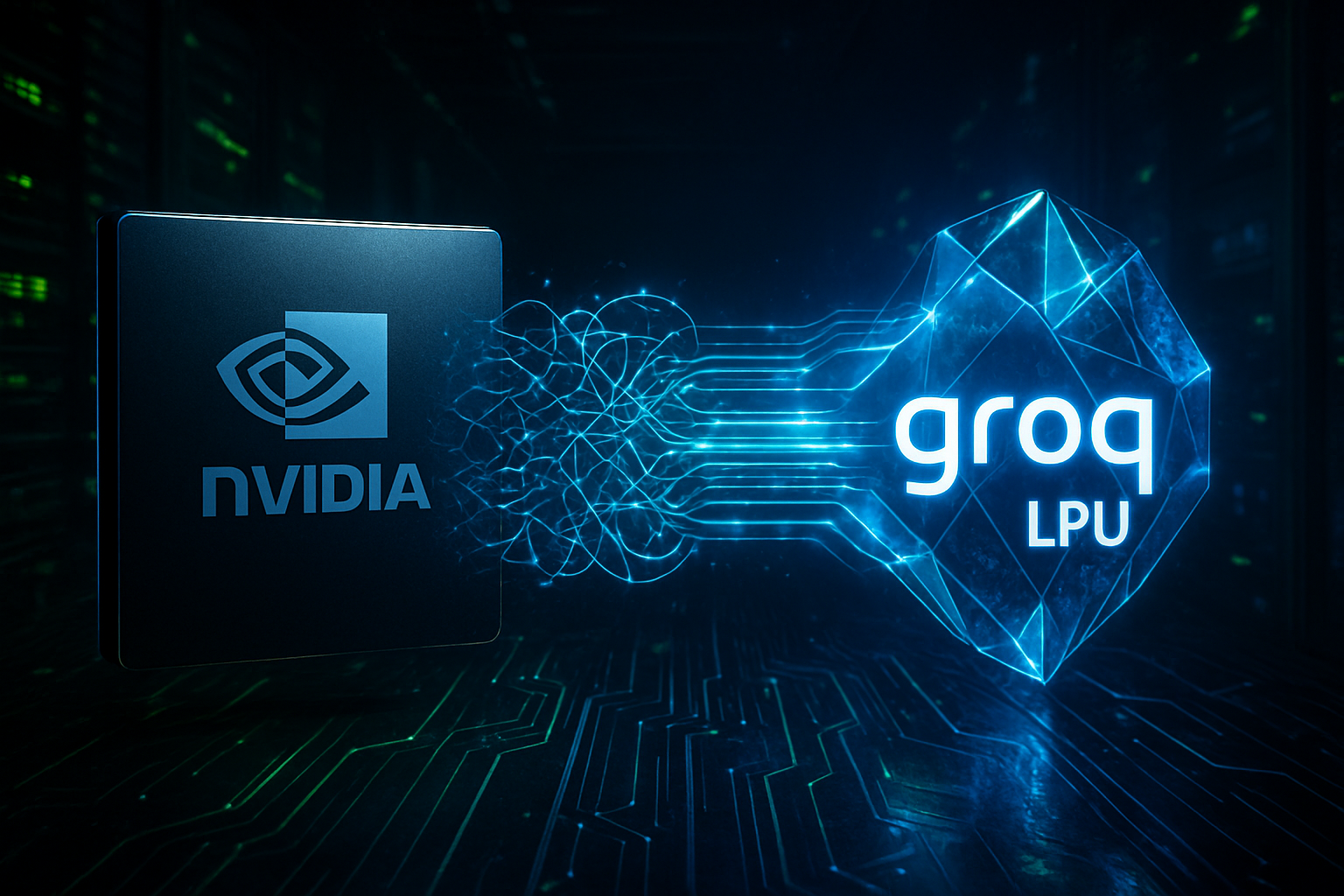
In a move that has sent shockwaves through Silicon Valley and the global semiconductor industry, Nvidia (NASDAQ: NVDA) finalized a landmark $20 billion asset and talent acquisition of the high-performance AI chip startup Groq in late December 2025. Announced on Christmas Eve, the deal represents one of the most significant strategic maneuvers in Nvidia’s history, effectively absorbing the industry’s leading low-latency inference technology and its world-class engineering team.
The acquisition is a decisive strike aimed at cementing Nvidia’s dominance as the artificial intelligence industry shifts its primary focus from training massive models to the "Inference Era"—the real-time execution of those models in consumer and enterprise applications. By bringing Groq’s revolutionary Language Processing Unit (LPU) architecture under its wing, Nvidia has not only neutralized its most formidable technical challenger but also secured a vital technological hedge against the ongoing global shortage of High Bandwidth Memory (HBM).
The LPU Breakthrough: Solving the Memory Wall
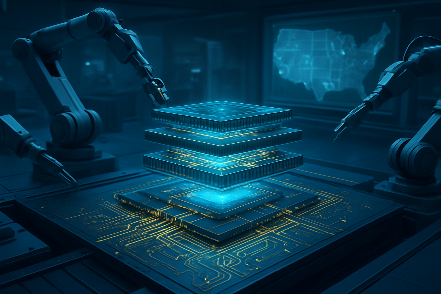
At the heart of this $20 billion deal is Groq’s proprietary LPU architecture, which has consistently outperformed traditional GPUs in real-time language tasks throughout 2024 and 2025. Unlike Nvidia’s current H100 and B200 chips, which rely on HBM to manage data, Groq’s LPUs utilize on-chip SRAM (Static Random-Access Memory). This fundamental architectural difference eliminates the "memory wall"—a bottleneck where the processor spends more time waiting for data to arrive from memory than actually performing calculations.
Technical specifications released during the acquisition reveal that Groq’s LPUs deliver nearly 10x the throughput of standard GPUs for Large Language Model (LLM) inference while consuming approximately 90% less power. This deterministic performance allows for the near-instantaneous token generation required for the next generation of interactive AI agents. Industry experts note that Nvidia plans to integrate this LPU logic directly into its upcoming "Vera Rubin" chip architecture, scheduled for a 2026 release, marking a radical evolution in Nvidia’s hardware roadmap.
Strengthening the Software Moat and Neutralizing Rivals
The acquisition is as much about software as it is about silicon. Nvidia is already moving to integrate Groq’s software libraries into its ubiquitous CUDA platform. This "dual-stack" strategy will allow developers to use a single programming environment to train models on Nvidia GPUs and then deploy them for ultra-fast inference on LPU-enhanced hardware. By folding Groq’s innovations into CUDA, Nvidia is making its software ecosystem even more indispensable to the AI industry, creating a formidable barrier to entry for competitors.
From a competitive standpoint, the deal effectively removes Groq from the board as an independent entity just as it was beginning to gain significant traction with major cloud providers. While companies like Advanced Micro Devices, Inc. (NASDAQ: AMD) and Intel Corporation (NASDAQ: INTC) have been racing to catch up to Nvidia’s training capabilities, Groq was widely considered the only startup with a credible lead in specialized inference hardware. By paying a 3x premium over Groq’s last private valuation, Nvidia has ensured that this technology—and the talent behind it, including Groq founder and TPU pioneer Jonathan Ross—stays within the Nvidia ecosystem.
Navigating the Shift to the Inference Era
The broader significance of this acquisition lies in the changing landscape of AI compute. In 2023 and 2024, the market was defined by a desperate "land grab" for training hardware as companies raced to build foundational models. However, by late 2025, the focus shifted toward the economics of running those models at scale. As AI moves into everyday devices and real-time assistants, the cost and latency of inference have become the primary concerns for tech giants and startups alike.
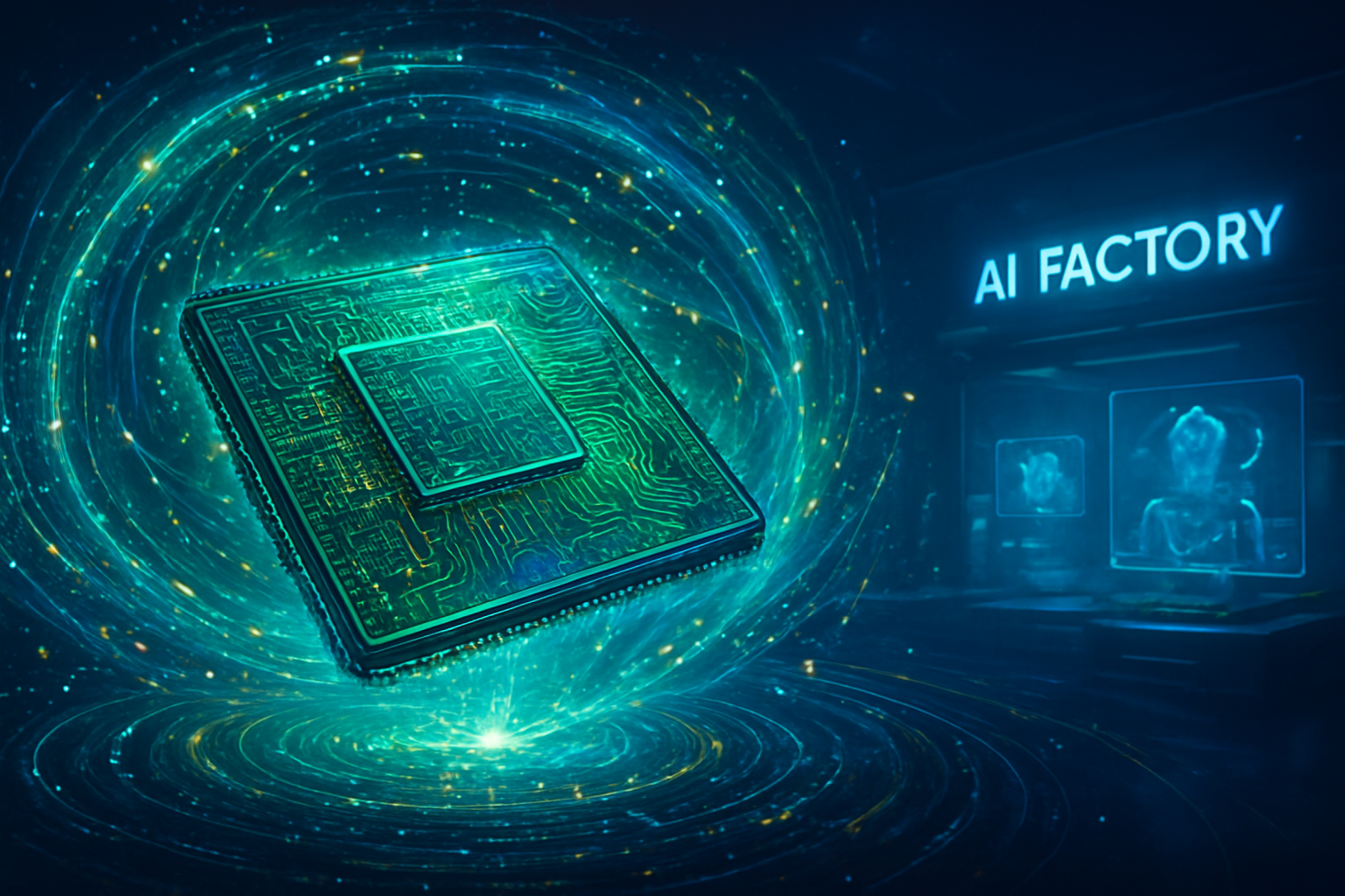
Nvidia’s move also addresses a critical vulnerability in the AI supply chain: the reliance on HBM. With HBM production capacity frequently strained by high demand from multiple chipmakers, Groq’s SRAM-based approach offers Nvidia a strategic alternative that does not depend on the same constrained manufacturing processes. This diversification of its hardware portfolio makes Nvidia’s "AI Factory" vision more resilient to the geopolitical and logistical shocks that have plagued the semiconductor industry in recent years.
The Road Ahead: Real-Time Agents and Vera Rubin
Looking forward, the integration of Groq’s technology is expected to accelerate the deployment of "Agentic AI"—autonomous systems capable of complex reasoning and real-time interaction. In the near term, we can expect Nvidia to launch specialized inference cards based on Groq’s designs, targeting the rapidly growing market for edge computing and private enterprise AI clouds.
The long-term play, however, is the Vera Rubin platform. Analysts predict that the 2026 chip generation will be the first to truly hybridize GPU and LPU architectures, creating a "universal AI processor" capable of handling both massive training workloads and ultra-low-latency inference on a single die. The primary challenge remaining for Nvidia will be navigating the inevitable antitrust scrutiny from regulators in the US and EU, who are increasingly wary of Nvidia’s near-monopoly on the "oxygen" of the AI economy.
A New Chapter in AI History
The acquisition of Groq marks the end of an era for AI hardware startups and the beginning of a consolidated phase where the "Big Three" of AI compute—Nvidia, and to a lesser extent, the custom silicon efforts of Microsoft (NASDAQ: MSFT) and Alphabet Inc. (NASDAQ: GOOGL)—vye for total control of the stack. By securing Jonathan Ross and his team, Nvidia has not only bought technology but also the visionary leadership that helped define the modern AI era at Google.
As we enter 2026, the key takeaway is clear: Nvidia is no longer just a "graphics" or "training" company; it has evolved into the definitive infrastructure provider for the entire AI lifecycle. The success of the Groq integration will be the defining story of the coming year, as the industry watches to see if Nvidia can successfully merge two distinct hardware philosophies into a single, unstoppable AI powerhouse.
This content is intended for informational purposes only and represents analysis of current AI developments.
TokenRing AI delivers enterprise-grade solutions for multi-agent AI workflow orchestration, AI-powered development tools, and seamless remote collaboration platforms.
For more information, visit https://www.tokenring.ai/.