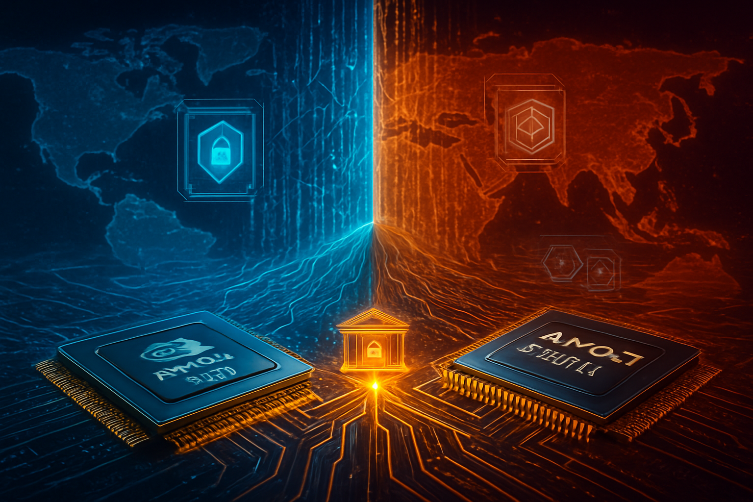
The semiconductor industry has officially entered a new era. As of February 2026, the long-predicted transition from organic packaging materials to glass substrates has moved from laboratory curiosity to a critical manufacturing reality. This shift marks the first major departure in decades from Ajinomoto Build-up Film (ABF), the industry-standard organic resin that has underpinned chip packaging since the 1990s. The move is not merely an incremental upgrade; it is a desperate and necessary response to the "Warpage Wall," a physical limitation that threatened to halt the scaling of the world’s most powerful AI accelerators.
For companies like NVIDIA Corporation (NASDAQ: NVDA) and Advanced Micro Devices, Inc. (NASDAQ: AMD), the glass breakthrough is the "oxygen" required for their next generation of hardware. By replacing organic cores with ultra-rigid glass, manufacturers are now able to package massive, multi-die chiplets that would have physically buckled under the heat and pressure of traditional manufacturing. This month, the first production-grade AI modules featuring glass-based architectures have begun shipping, signaling a fundamental change in how the silicon brains of the AI revolution are built.
Shattering the Warpage Wall: The Technical Leap Forward
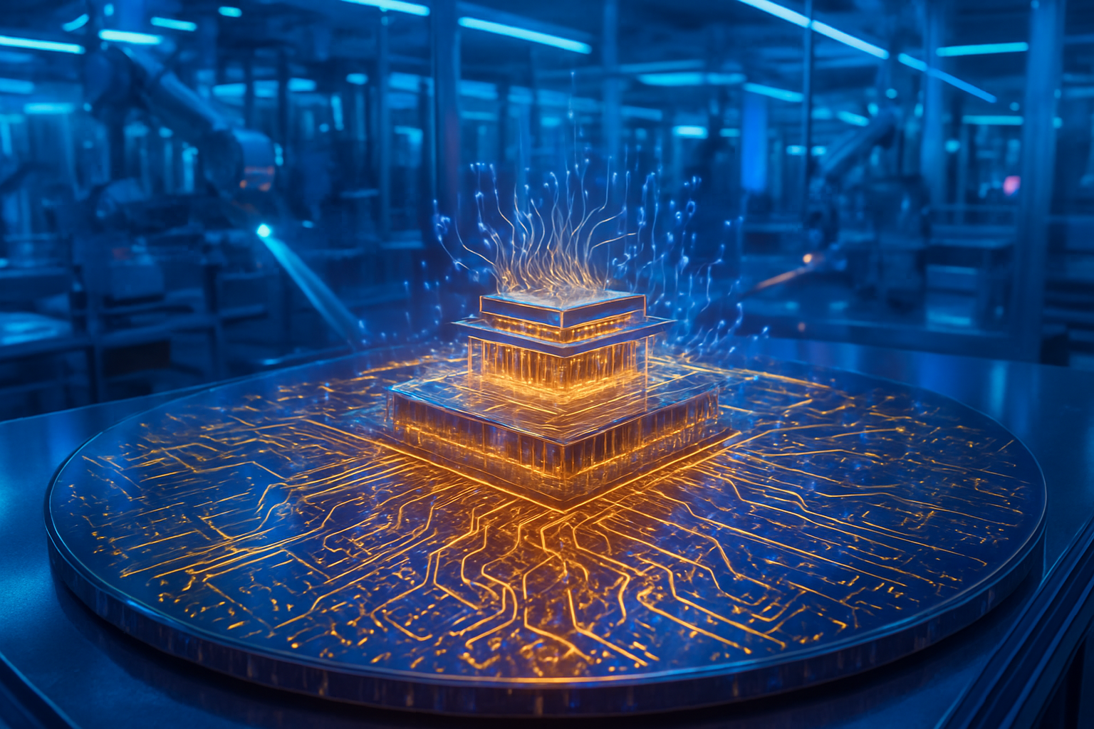
The technical driver behind this transition is a phenomenon known as the "Warpage Wall." As AI accelerators grow larger to accommodate more transistors and High Bandwidth Memory (HBM), the thermal expansion differences between silicon and organic ABF substrates become catastrophic. At the extreme operating temperatures of modern data centers, organic materials expand and contract at rates far different from the silicon chips they support. This leads to "warping"—a physical bending of the package that snaps microscopic interconnects and craters manufacturing yields. Glass, however, possesses a Coefficient of Thermal Expansion (CTE) that nearly matches silicon. This thermal harmony allows for a 50% reduction in warpage, enabling the creation of packages that are twice the size of current lithography limits, reaching up to 1,700 mm².
Beyond thermal stability, glass offers a level of flatness that organic materials cannot replicate. Glass substrates are approximately three times flatter than their organic counterparts, providing a superior foundation for advanced lithography. This extreme flatness allows for the deployment of ultra-fine Redistribution Layers (RDL) with features smaller than 2µm. Furthermore, glass is an exceptional insulator with a low dielectric constant, which reduces signal interference and power loss. Early benchmarks from February 2026 indicate that chips using glass substrates are achieving a 30% to 50% improvement in power efficiency—a critical metric for the power-hungry AI industry.
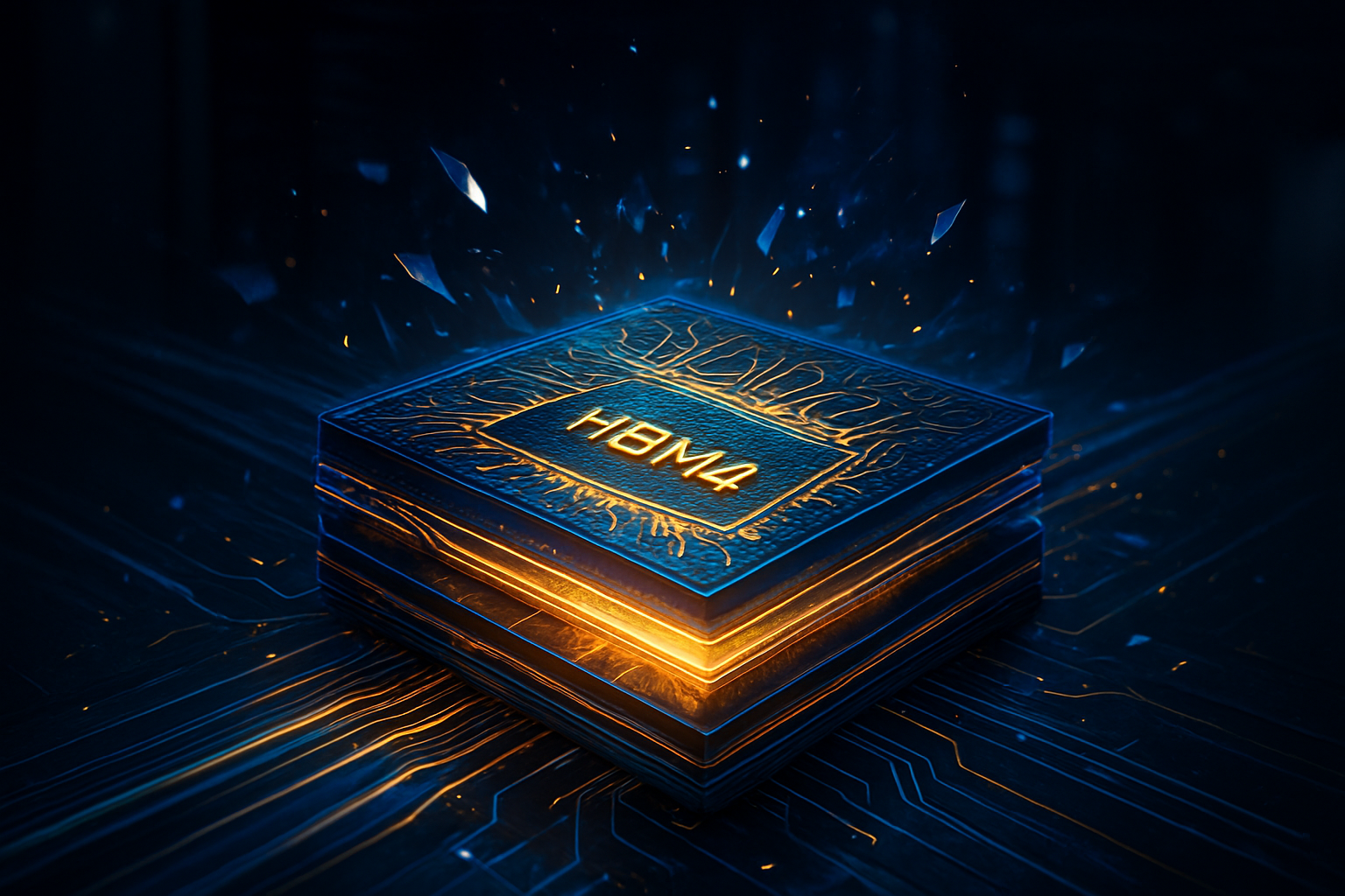
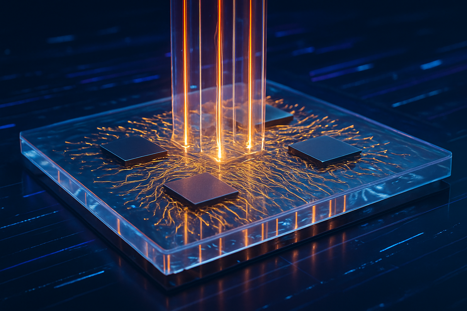
The "holy grail" of this advancement is the Through-Glass Via (TGV). While traditional organic substrates rely on mechanical drilling that is limited to a roughly 325µm pitch, glass allows for laser-induced etching to create vias at a pitch of 100µm or less. Because density scales quadratically with pitch, this move from 325µm to 100µm delivers a staggering 10.56x increase in interconnect density. This enables up to 50,000 I/O connections per package, providing the massive vertical power delivery and data throughput required by the high-current demands of the newest GPU architectures.
The Corporate Race for Glass Supremacy
The competitive landscape of the semiconductor industry has been jolted by this transition, with Intel Corporation (NASDAQ: INTC) currently leading the charge. In late January 2026, Intel unveiled its first mass-market CPU featuring a glass core, the Xeon 6+ "Clearwater Forest." This achievement followed years of R&D at its Chandler, Arizona facility. By successfully implementing a "thick-core" 10-2-10 architecture—ten RDL layers on each side of a 1.6mm glass core—Intel has positioned itself as the primary architect of the glass era, leveraging its internal packaging capabilities to gain a strategic advantage over competitors who rely solely on external foundries.
However, the competition is fierce. SK Hynix Inc. (KRX: 000660), through its specialized subsidiary Absolics, has become the first to achieve large-scale commercialization for third-party clients. Operating out of a new $600 million facility in Georgia, USA, Absolics is already supplying glass substrate samples to AMD and Amazon.com, Inc. (NASDAQ: AMZN) for their custom AI silicon. Meanwhile, Samsung Electronics (KRX: 000660) has mobilized its "Triple Alliance"—integrating its electronics, display, and electro-mechanics divisions—to accelerate its own glass production. Samsung shifted its glass project to a dedicated Commercialization Unit this month, aiming to capture the high-end System-in-Package (SiP) market by the end of 2026.
Taiwan Semiconductor Manufacturing Company (NYSE: TSM) is taking a slightly different but equally ambitious path. TSMC is focusing on Panel-Level Packaging (PLP) using rectangular glass panels as large as 750x620mm. This approach, known as CoPoS (Chip-on-Panel-on-Substrate), aims to maximize area utilization and lower costs for the massive scale required by the upcoming "Vera Rubin" architecture from NVIDIA. While Intel and SK Hynix are ahead in immediate deployments, TSMC’s panel-level scale could define the cost structure of the industry by 2027 and 2028.
A Fundamental Shift in the AI Landscape
The adoption of glass substrates is more than a packaging upgrade; it is the physical realization of "More than Moore." As traditional transistor scaling slows down, the industry has turned to "system-level" scaling. Glass provides the rigid backbone necessary to stitch together dozens of chiplets into a single, massive compute engine. Without glass, the thermal and mechanical stresses of modern AI chips would have hit a hard ceiling, potentially stalling the progress of Large Language Models (LLMs) and generative AI research that depends on ever-more-powerful hardware.
This breakthrough also has significant implications for data center efficiency and environmental sustainability. The 30-50% reduction in power consumption afforded by glass’s superior electrical properties arrives at a time when AI energy demand is under intense global scrutiny. By reducing signal loss and improving thermal management, glass substrates allow data centers to pack more compute density into the same physical footprint without an exponential increase in cooling requirements. This makes the "Glass Age" a pivotal moment in the transition toward more sustainable high-performance computing.
However, the transition is not without its risks. The move to glass requires a complete overhaul of the packaging supply chain. Traditional substrate makers who cannot pivot from organic materials risk obsolescence. Furthermore, the brittleness of glass poses unique handling challenges during the manufacturing process, and while yields are improving—Absolics reports levels between 75% and 85%—they still lag behind the mature organic processes of yesteryear. The industry is effectively "re-learning" how to build chips, a process that carries significant capital risk.
The Horizon: From AI Accelerators to Optical Integration
Looking ahead, the roadmap for glass substrates extends far beyond simple GPU packaging. Experts predict that by 2028, the industry will begin integrating Co-Packaged Optics (CPO) directly onto glass substrates. Because glass is transparent and can be etched with high precision, it is the ideal medium for routing both electrical signals and light. This could lead to a future where chip-to-chip communication happens via on-package lasers and waveguides, virtually eliminating the latency and power bottlenecks of copper wiring.
We also expect to see "Glass-First" designs for consumer electronics. While the current focus is on $40,000 AI GPUs, the mechanical benefits of glass—allowing for thinner, more rigid, and more thermally efficient devices—will eventually trickle down to high-end laptops and smartphones. As manufacturing yields stabilize throughout 2026 and 2027, the "Glass Age" will move from the data center to the pocket. The next milestone to watch will be the full-scale deployment of NVIDIA’s Rubin platform, which is expected to be the ultimate proof-of-concept for the viability of glass at the highest levels of global computing.
Conclusion: A New Foundation for Intelligence
The breakthrough of glass substrates in February 2026 marks a watershed moment in semiconductor history. By overcoming the "Warpage Wall," the industry has cleared the path for the next decade of AI scaling, ensuring that the physical limitations of organic materials do not hinder the digital aspirations of the AI research community. The transition reflects a broader trend in the tech industry: when software demands reach the limits of physics, the industry innovates its way into entirely new materials.
As we look toward the remainder of 2026, the primary indicators of success will be the production yields at the new glass facilities in Arizona and Georgia, and the thermal performance of the first "Clearwater Forest" and "Rubin" chips in the wild. The silicon era has not ended, but it has found a new, clearer foundation. The "Glass Age" is no longer a future prediction—it is the operational reality of the global AI economy.
This content is intended for informational purposes only and represents analysis of current AI developments.
TokenRing AI delivers enterprise-grade solutions for multi-agent AI workflow orchestration, AI-powered development tools, and seamless remote collaboration platforms.
For more information, visit https://www.tokenring.ai/.