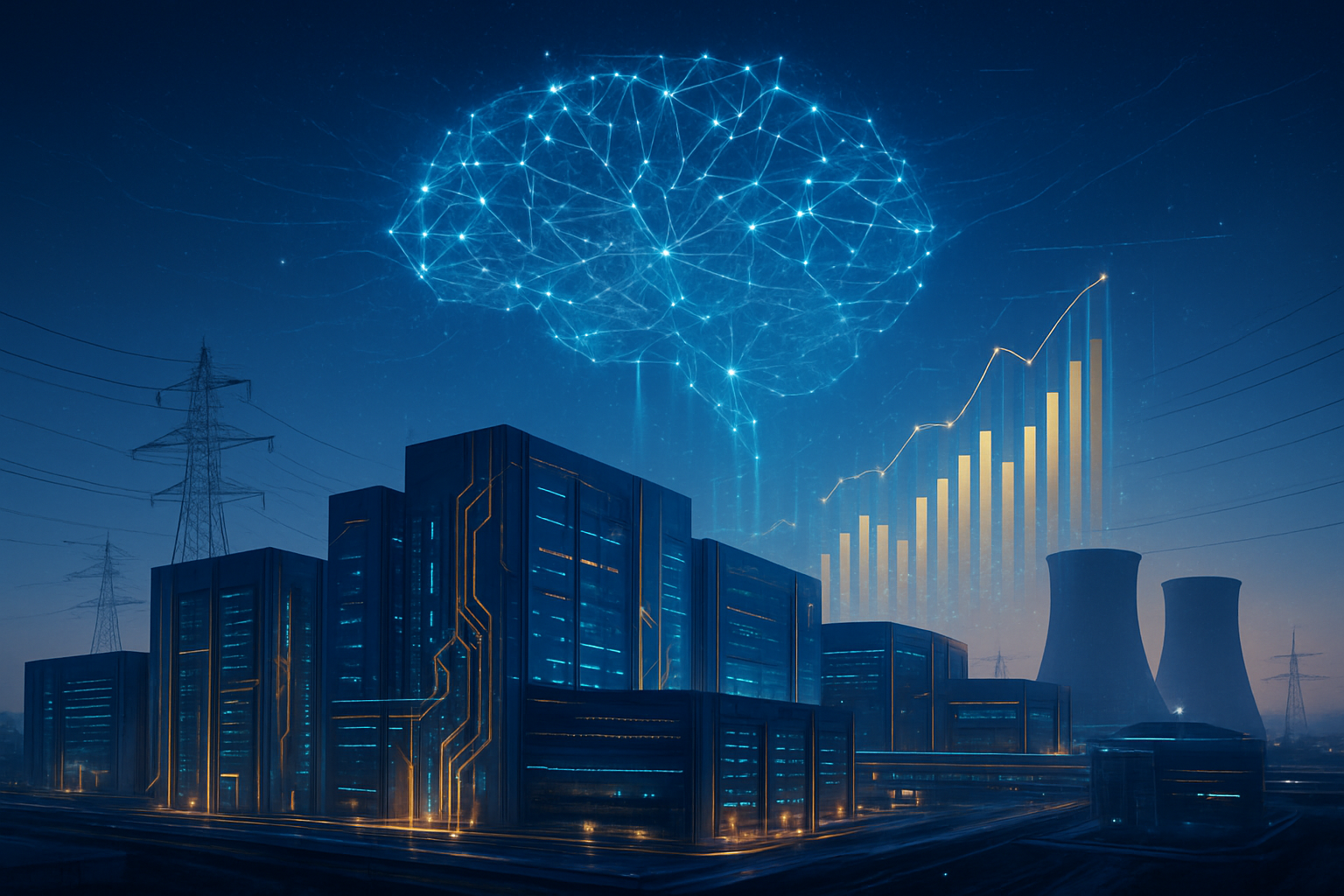
As 2025 draws to a close, the final economic post-mortems reveal a startling reality: the United States economy has become structurally dependent on the artificial intelligence revolution. According to a landmark year-end analysis of Bureau of Economic Analysis (BEA) data, investment in AI-related equipment and software was responsible for a staggering 92% of all U.S. GDP growth during the first half of the year. This shift marks the most significant sectoral concentration of economic expansion in modern history, positioning AI not just as a technological trend, but as the primary life-support system for national prosperity.
The report, spearheaded by Harvard economist and former Council of Economic Advisers Chair Jason Furman, highlights a "dangerously narrow" growth profile. While the headline GDP figures remained resilient throughout 2025, the underlying data suggests that without the massive capital expenditures from tech titans, the U.S. would have faced a year of near-stagnation. This "AI-driven GDP" phenomenon has redefined the relationship between Silicon Valley and Wall Street, as the physical construction of data centers and the procurement of high-end semiconductors effectively "saved" the 2025 economy from a widely predicted recession.
The Infrastructure Arms Race
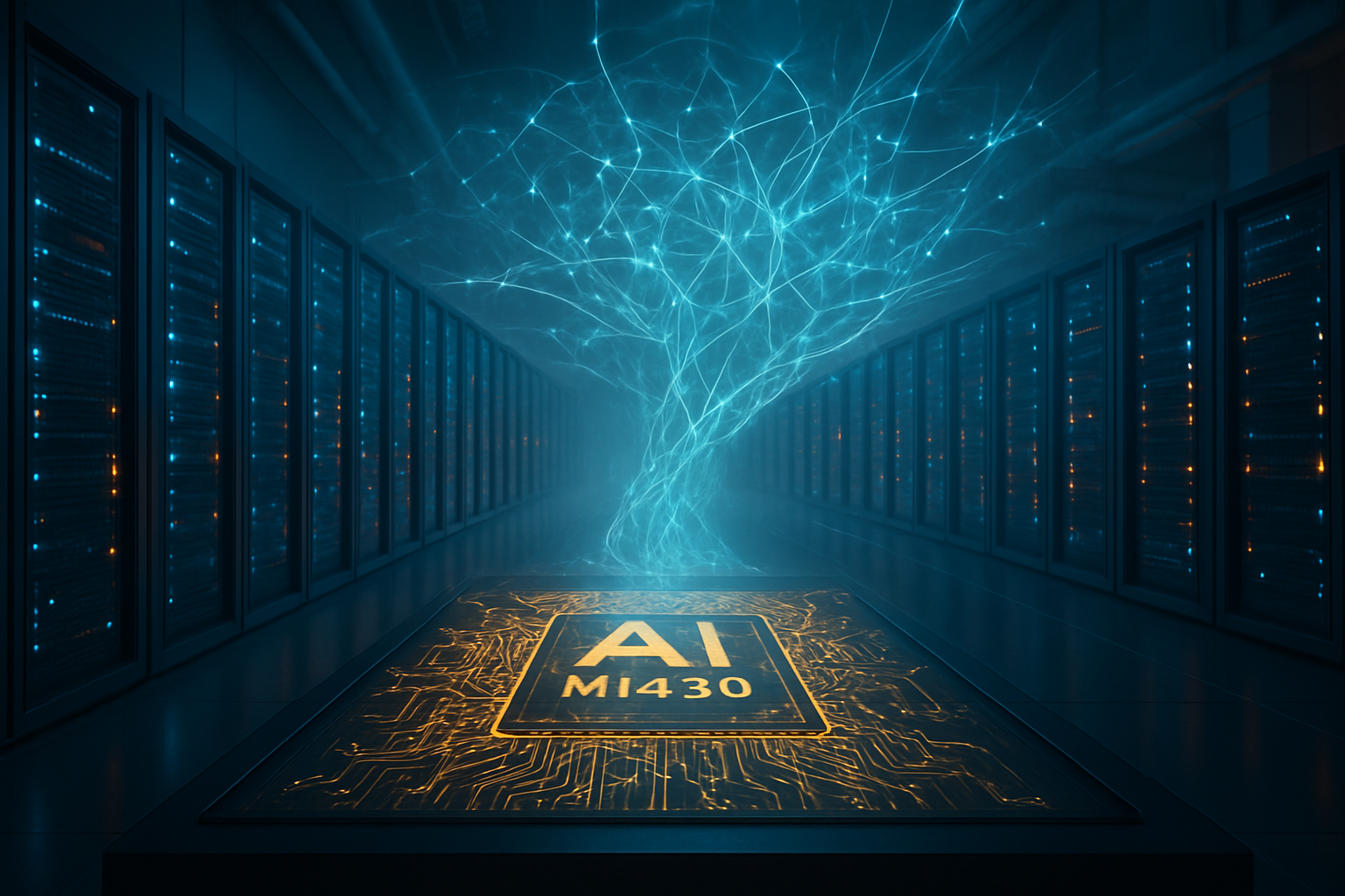
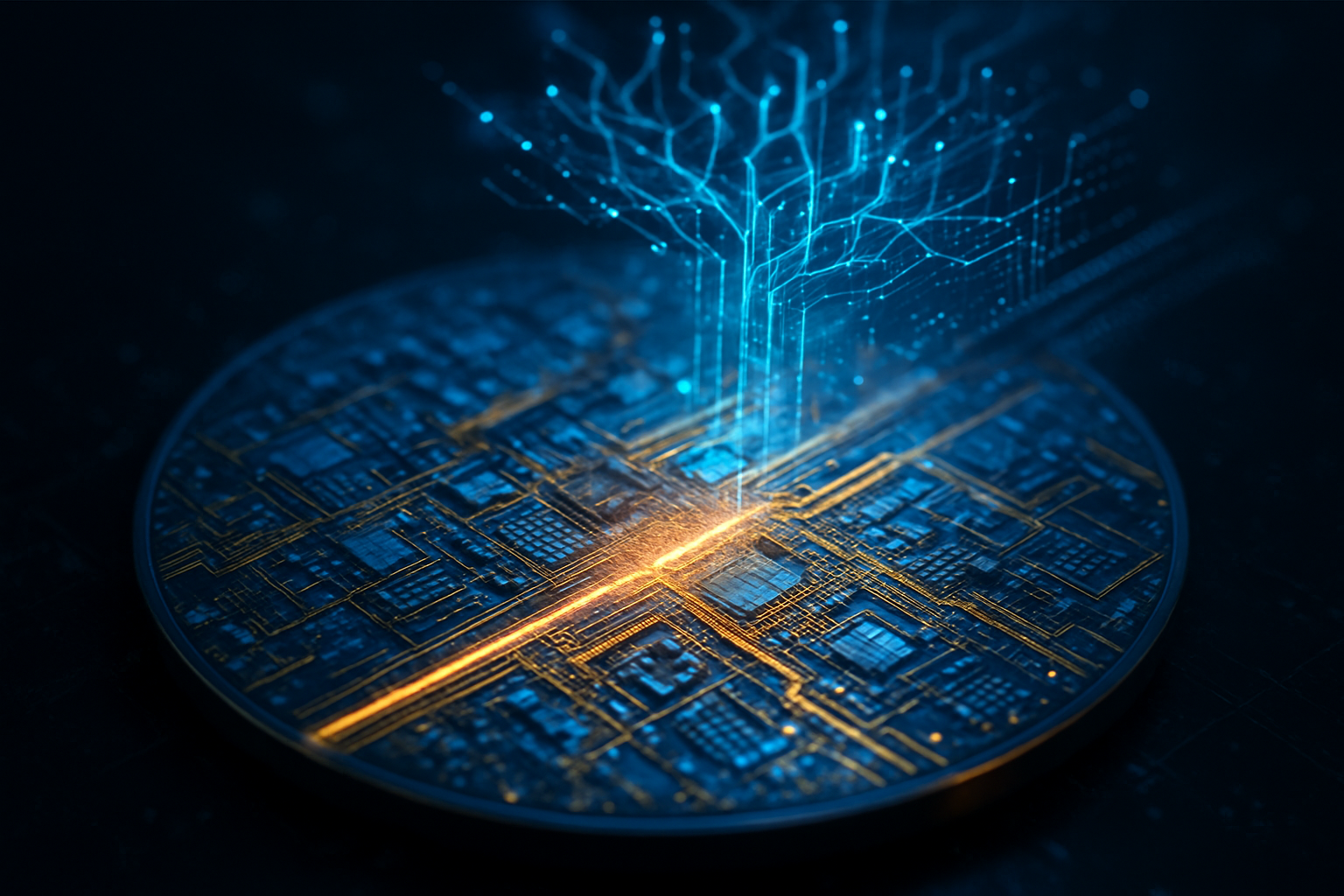
The technical foundation of this economic surge lies in a massive "arms race" for specialized hardware and high-density infrastructure. The Furman report specifically cites a 39% annualized growth rate in the "information processing equipment and software" category during the first half of 2025. This growth was driven by the rollout of next-generation silicon, most notably the Blackwell architecture from Nvidia (NASDAQ: NVDA), which saw its market capitalization cross the $5 trillion threshold this year. Unlike previous tech cycles where software drove value, 2025 was the year of "hard infra," characterized by the deployment of massive GPU clusters and custom AI accelerators like Alphabet's (NASDAQ: GOOGL) TPU v6.
Technically, the shift in 2025 was defined by the transition from model training to large-scale inference. While 2024 focused on building the "brains" of AI, 2025 saw the construction of the "nervous system"—the global infrastructure required to run these models for hundreds of millions of users simultaneously. This necessitated a new class of data centers, such as Microsoft's (NASDAQ: MSFT) "Fairwater" facility, which utilizes advanced liquid cooling and modular power designs to support power densities exceeding 100 kilowatts per rack. These specifications are a quantum leap over the 10-15 kW standards of the previous decade, representing a total overhaul of the nation's industrial computing capacity.
Industry experts and the AI research community have reacted to these findings with a mix of awe and trepidation. While the technical achievements in scaling are unprecedented, many researchers argue that the "92% figure" reflects a massive front-loading of hardware that has yet to be fully utilized. The sheer volume of compute power now coming online has led to what Microsoft CEO Satya Nadella recently termed a "model overhang"—a state where the raw capabilities of the hardware and the models themselves have temporarily outpaced the ability of enterprises to integrate them into daily workflows.
Hyper-Scale Hegemony and Market Dynamics
The implications for the technology sector have been transformative, cementing a "Hyper-Scale Hegemony" among a handful of firms. Amazon (NASDAQ: AMZN) led the charge in capital expenditure, projecting a total spend of up to $125 billion for 2025, largely dedicated to its "Project Rainier" initiative—a network of 30 massive AI-optimized data centers. This level of spending has created a significant barrier to entry, as even well-funded startups struggle to compete with the sheer physical footprint and energy procurement capabilities of the "Big Five." Meta (NASDAQ: META) similarly surprised analysts by increasing its 2025 capex to over $70 billion, doubling down on open-source Llama models to commoditize the underlying AI software while maintaining control over the hardware layer.
This environment has also birthed massive private-public partnerships, most notably the $500 billion "Project Stargate" initiative involving OpenAI and Oracle (NYSE: ORCL). This venture represents a strategic pivot toward multi-gigawatt supercomputing networks that operate almost like sovereign utilities. For major AI labs, the competitive advantage has shifted from who has the best algorithm to who has the most reliable access to power and cooling. This has forced companies like Apple (NASDAQ: AAPL) to deepen their infrastructure partnerships, as the local "on-device" AI processing of 2024 gave way to a hybrid model requiring massive cloud-based "Private Cloud Compute" clusters to handle more complex reasoning tasks.
However, this concentration of growth has raised concerns about market fragility. Financial institutions like JPMorgan Chase (NYSE: JPM) have warned of a "boom-bust" risk if the return on investment (ROI) for these trillion-dollar expenditures does not materialize by mid-2026. While the "picks and shovels" providers like Nvidia have seen record profits, the "application layer"—the startups and enterprises using AI to sell products—is under increasing pressure to prove that AI can generate new revenue streams rather than just reducing costs through automation.
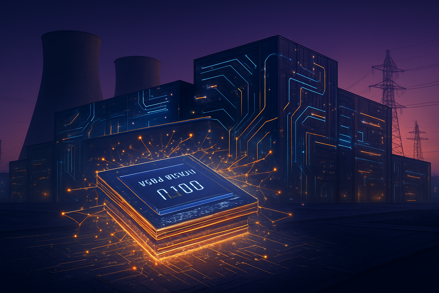
The Broader Landscape: Power and Labor
Beyond the balance sheets, the wider significance of the 2025 AI boom is being felt in the very fabric of the U.S. power grid and labor market. The primary bottleneck for AI growth in 2025 shifted from chip availability to electricity. Data center energy demand has reached such heights that it is now a significant factor in national energy policy, driving a resurgence in nuclear power investments and causing utility price spikes in tech hubs like Northern Virginia. This has led to a "K-shaped" economic reality: while AI infrastructure drives GDP, it does not necessarily drive widespread employment. Data centers are capital-intensive but labor-light, meaning the 92% GDP contribution has not translated into a proportional surge in middle-class job creation.
Economists at Goldman Sachs (NYSE: GS) have introduced the concept of "Invisible GDP" to describe the current era. They argue that traditional metrics may actually be undercounting AI's impact because much of the value—such as increased coding speed for software engineers or faster drug discovery—is treated as an intermediate input rather than a final product. Conversely, Bank of America (NYSE: BAC) analysts point to an "Import Leak," noting that while AI investment boosts U.S. GDP, a significant portion of that capital flows overseas to semiconductor fabrication plants in Taiwan and assembly lines in Southeast Asia, which could dampen the long-term domestic multiplier effect.
This era also mirrors previous industrial milestones, such as the railroad boom of the 19th century or the build-out of the fiber-optic network in the late 1990s. Like those eras, 2025 has been defined by "over-building" in anticipation of future demand. The concern among some historians is that while the infrastructure will eventually be transformative, the "financial indigestion" following such a rapid build-out could lead to a significant market correction before the full benefits of AI productivity are realized by the broader public.
The 2026 Horizon: From Building to Using
Looking toward 2026, the focus is expected to shift from "building" to "using." Experts predict that the next 12 to 18 months will be the "Year of ROI," where the market will demand proof that the trillions spent on infrastructure can translate into bottom-line corporate profits beyond the tech sector. We are already seeing the horizon of "Agentic AI"—systems capable of executing complex, multi-step business processes autonomously—which many believe will be the "killer app" that justifies the 2025 spending spree. If these agents can successfully automate high-value tasks in legal, medical, and financial services, the 2025 infrastructure boom will be seen as a masterstroke of foresight.
However, several challenges remain on the horizon. Regulatory scrutiny is intensifying, with both U.S. and EU authorities looking closely at the energy consumption of data centers and the competitive advantages held by the hyperscalers. Furthermore, the transition to Artificial General Intelligence (AGI) remains a wildcard. Sam Altman of OpenAI has hinted that 2026 could see the arrival of systems capable of "novel insights," a development that would fundamentally change the economic calculus of AI from a productivity tool to a primary generator of new knowledge and intellectual property.
Conclusion: A Foundation for the Future
The economic story of 2025 is one of unprecedented concentration and high-stakes betting. By accounting for 92% of U.S. GDP growth in the first half of the year, AI infrastructure has effectively become the engine of the American economy. This development is a testament to the transformative power of generative AI, but it also serves as a reminder of the fragility that comes with such narrow growth. The "AI-driven GDP" has provided a crucial buffer against global economic headwinds, but it has also set a high bar for the years to follow.
As we enter 2026, the world will be watching to see if the massive digital cathedrals built in 2025 can deliver on their promise. The significance of this year in AI history cannot be overstated; it was the year the "AI Summer" turned into a permanent industrial season. Whether this leads to a sustained era of hyper-productivity or a painful period of consolidation will be the defining question of the next decade. For now, the message from 2025 is clear: the AI revolution is no longer a future prospect—it is the foundation upon which the modern economy now stands.
This content is intended for informational purposes only and represents analysis of current AI developments.
TokenRing AI delivers enterprise-grade solutions for multi-agent AI workflow orchestration, AI-powered development tools, and seamless remote collaboration platforms.
For more information, visit https://www.tokenring.ai/.