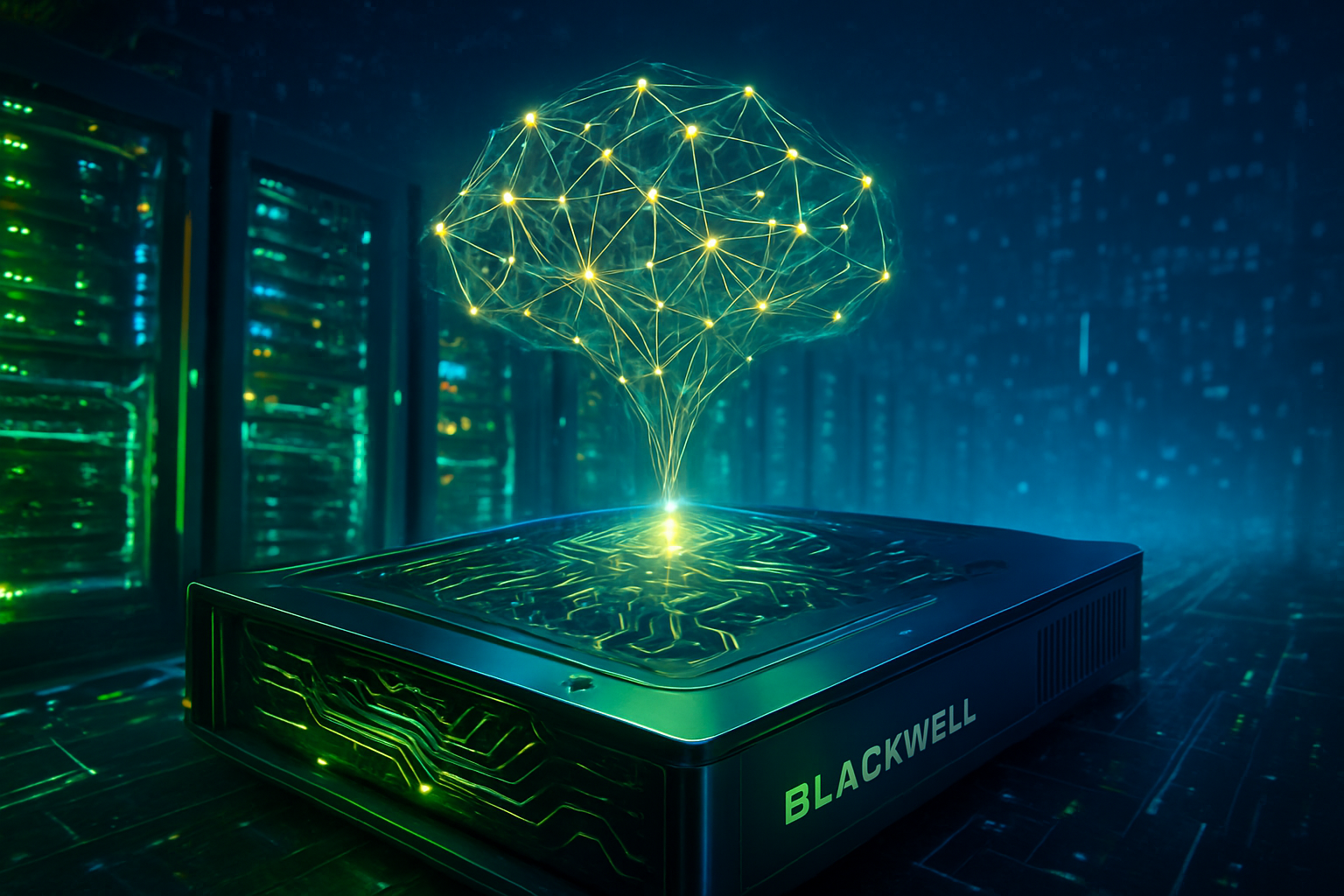
In a move that has sent shockwaves through Silicon Valley and global markets, Nvidia (NASDAQ: NVDA) has finalized a staggering $20 billion strategic intellectual property (IP) deal with the AI chip sensation Groq. Beyond the massive capital outlay, the deal includes the high-profile hiring of Groq’s visionary founder, Jonathan Ross, and nearly 80% of the startup’s engineering talent. This "license-and-acquihire" maneuver signals a definitive shift in Nvidia’s strategy, as the company moves to consolidate its dominance over the burgeoning AI inference market.
The deal, announced as we close out 2025, represents a pivotal moment in the hardware arms race. While Nvidia has long been the undisputed king of AI "training"—the process of building massive models—the industry’s focus has rapidly shifted toward "inference," the actual running of those models for end-users. By absorbing Groq’s specialized Language Processing Unit (LPU) technology and the mind of the man who originally led Google’s (NASDAQ: GOOGL) TPU program, Nvidia is positioning itself to own the entire AI lifecycle, from the first line of code to the final millisecond of a user’s query.
The LPU Advantage: Solving the Memory Bottleneck
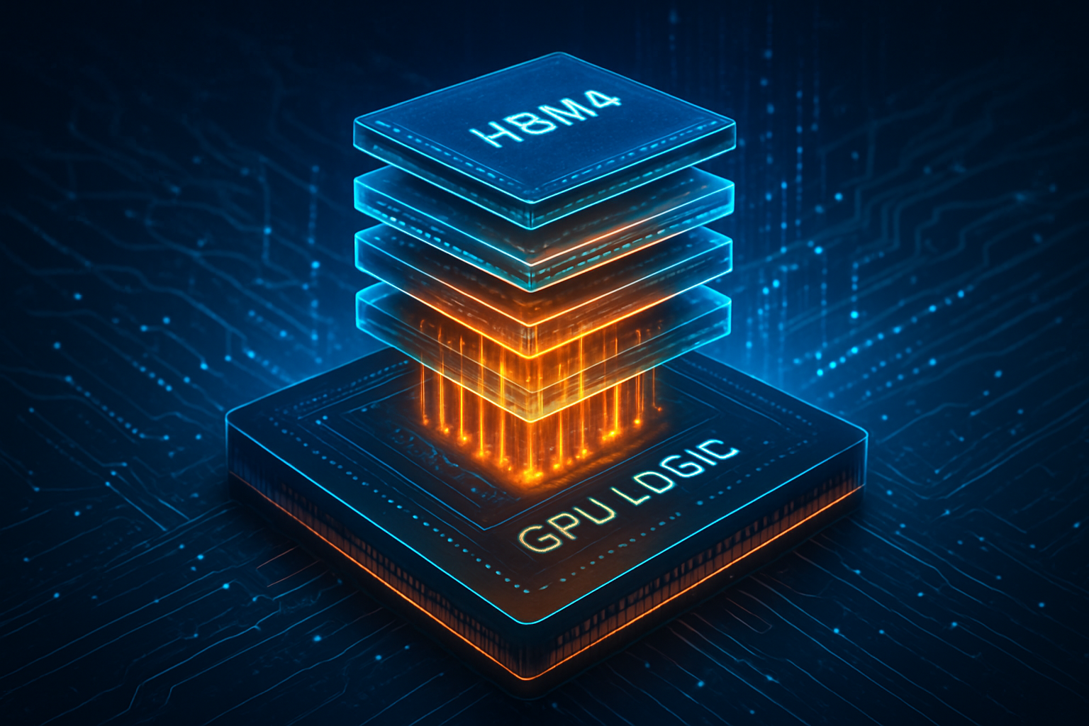
At the heart of this deal is Groq’s radical LPU architecture, which differs fundamentally from the GPU (Graphics Processing Unit) architecture that propelled Nvidia to its multi-trillion-dollar valuation. Traditional GPUs rely on High Bandwidth Memory (HBM), which, while powerful, creates a "Von Neumann bottleneck" during inference. Data must travel between the processor and external memory stacks, causing latency that can hinder real-time AI interactions. In contrast, Groq’s LPU utilizes massive amounts of on-chip SRAM (Static Random-Access Memory), allowing model weights to reside directly on the processor.
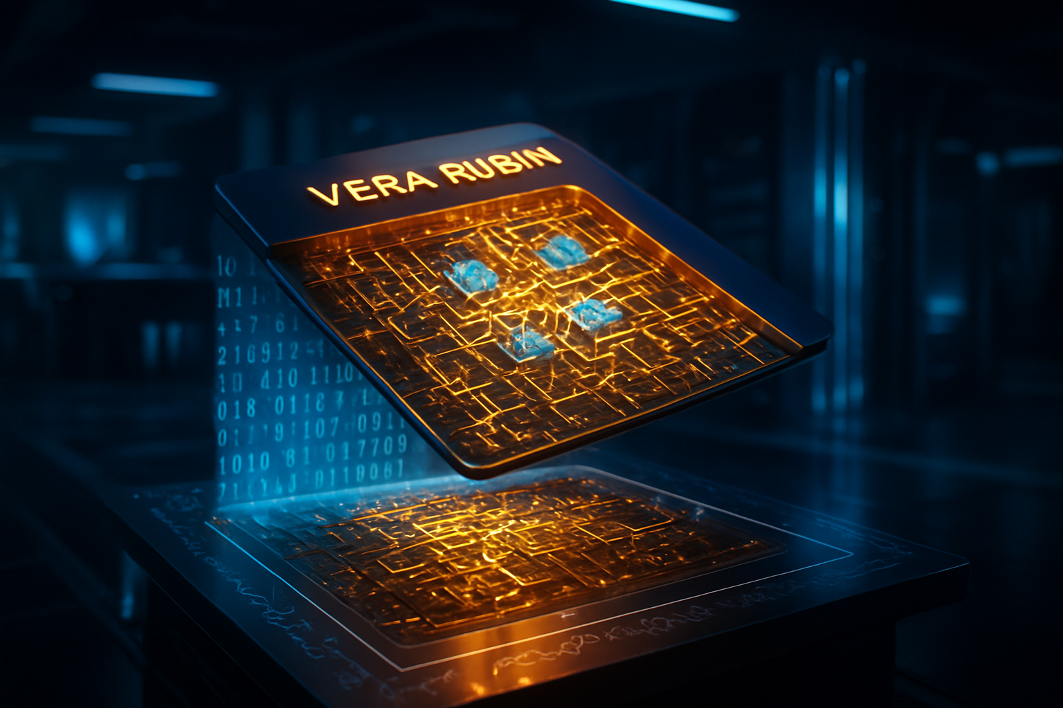
The technical specifications of this integration are formidable. Groq’s architecture provides a deterministic execution model, meaning the performance is mathematically predictable to the nanosecond—a far cry from the "jitter" or variable latency found in probabilistic GPU scheduling. By integrating this into Nvidia’s upcoming "Vera Rubin" chip architecture, experts predict token-generation speeds could jump from the current 100 tokens per second to over 500 tokens per second for models like Llama 3. This enables "Batch Size 1" processing, where a single user receives an instantaneous response without the need for the system to wait for other requests to fill a queue.
Initial reactions from the AI research community have been a mix of awe and apprehension. Dr. Elena Rodriguez, a senior fellow at the AI Hardware Institute, noted, "Nvidia isn't just buying a faster chip; they are buying a different way of thinking about compute. The deterministic nature of the LPU is the 'holy grail' for real-time applications like autonomous robotics and high-frequency trading." However, some industry purists worry that such consolidation may stifle the architectural diversity that has fueled recent innovation.
A Strategic Masterstroke: Market Positioning and Antitrust Maneuvers
The structure of the deal—a $20 billion IP license combined with a mass hiring event—is a calculated effort to bypass the regulatory hurdles that famously tanked Nvidia’s attempt to acquire ARM in 2022. By not acquiring Groq Inc. as a legal entity, Nvidia avoids the protracted 18-to-24-month antitrust reviews from global regulators. This "hollow-out" strategy, pioneered by Microsoft (NASDAQ: MSFT) and Amazon (NASDAQ: AMZN) earlier in the decade, allows Nvidia to secure the technology and talent it needs while leaving a shell of the original company to manage its existing "GroqCloud" service.
For competitors like AMD (NASDAQ: AMD) and Intel (NASDAQ: INTC), this deal is a significant blow. AMD had recently made strides in the inference space with its MI300 series, but the integration of Groq’s LPU technology into the CUDA ecosystem creates a formidable barrier to entry. Nvidia’s ability to offer ultra-low-latency inference as a native feature of its hardware stack makes it increasingly difficult for startups or established rivals to argue for a "specialized" alternative.
Furthermore, this move neutralizes one of the most credible threats to Nvidia’s cloud dominance. Groq had been rapidly gaining traction among developers who were frustrated by the high costs and latency of running large language models (LLMs) on standard GPUs. By bringing Jonathan Ross into the fold, Nvidia has effectively removed the "father of the TPU" from the competitive board, ensuring his next breakthroughs happen under the Nvidia banner.
The Inference Era: A Paradigm Shift in AI
The wider significance of this deal cannot be overstated. We are witnessing the end of the "Training Era" and the beginning of the "Inference Era." In 2023 and 2024, the primary constraint on AI was the ability to build models. In 2025, the constraint is the ability to run them efficiently, cheaply, and at scale. Groq’s LPU technology is significantly more energy-efficient for inference tasks than traditional GPUs, addressing a major concern for data center operators and environmental advocates alike.
This milestone is being compared to the 2006 launch of CUDA, the software platform that originally transformed Nvidia from a gaming company into an AI powerhouse. Just as CUDA made GPUs programmable for general tasks, the integration of LPU architecture into Nvidia’s stack makes real-time, high-speed AI accessible for every enterprise. It marks a transition from AI being a "batch process" to AI being a "living interface" that can keep up with human thought and speech in real-time.
However, the consolidation of such critical IP raises concerns about a "hardware monopoly." With Nvidia now controlling both the training and the most efficient inference paths, the tech industry must grapple with the implications of a single entity holding the keys to the world’s AI infrastructure. Critics argue that this could lead to higher prices for cloud compute and a "walled garden" that forces developers into the Nvidia ecosystem.
Looking Ahead: The Future of Real-Time Agents
In the near term, expect Nvidia to release a series of "Inference-First" modules designed specifically for edge computing and real-time voice and video agents. These products will likely leverage the newly acquired LPU IP to provide human-like interaction speeds in devices ranging from smart glasses to industrial robots. Jonathan Ross is reportedly leading a "Special Projects" division at Nvidia, tasked with merging the LPU’s deterministic pipeline with Nvidia’s massive parallel processing capabilities.
The long-term applications are even more transformative. We are looking at a future where AI "agents" can reason and respond in milliseconds, enabling seamless real-time translation, complex autonomous decision-making in split-second scenarios, and personalized AI assistants that feel truly instantaneous. The challenge will be the software integration; porting the world’s existing AI models to a hybrid GPU-LPU architecture will require a massive update to the CUDA toolkit, a task that Ross’s team is expected to spearhead throughout 2026.
A New Chapter for the AI Titan
Nvidia’s $20 billion bet on Groq is more than just an acquisition of talent; it is a declaration of intent. By securing the most advanced inference technology on the market, CEO Jensen Huang has shored up the one potential weakness in Nvidia’s armor. The "license-and-acquihire" model has proven to be an effective, if controversial, tool for market leaders to stay ahead of the curve while navigating a complex regulatory environment.
As we move into 2026, the industry will be watching closely to see how quickly the "Groq-infused" Nvidia hardware hits the market. This development will likely be remembered as the moment when the "Inference Gap" was closed, paving the way for the next generation of truly interactive, real-time artificial intelligence. For now, Nvidia remains the undisputed architect of the AI age, with a lead that looks increasingly insurmountable.
This content is intended for informational purposes only and represents analysis of current AI developments.
TokenRing AI delivers enterprise-grade solutions for multi-agent AI workflow orchestration, AI-powered development tools, and seamless remote collaboration platforms.
For more information, visit https://www.tokenring.ai/.