In a year defined by the transition from digital assistants to autonomous reasoning agents, Time Magazine has officially named "The Architects of AI" as its 2025 Person of the Year. The announcement, released on December 11, 2025, marks a pivotal moment in cultural history, recognizing a collective of engineers, CEOs, and researchers who have moved artificial intelligence from a speculative Silicon Valley trend into the foundational infrastructure of global society. Time Editor-in-Chief Sam Jacobs noted that the choice reflects a year in which AI's "full potential roared into view," making it clear that for the modern world, there is "no turning back or opting out."
The 2025 honor is not bestowed upon the software itself, but rather the individuals and organizations that "imagined, designed, and built the intelligence era." Featured on the cover are titans of the industry including Jensen Huang of NVIDIA (NASDAQ: NVDA), Sam Altman of OpenAI, and Dr. Fei-Fei Li of World Labs. This recognition comes as the world grapples with the sheer scale of AI’s integration, from the $500 billion "Stargate" data center projects to the deployment of models capable of solving complex mathematical proofs and autonomously managing corporate workflows.
The Dawn of 'System 2' Reasoning: Technical Breakthroughs of 2025
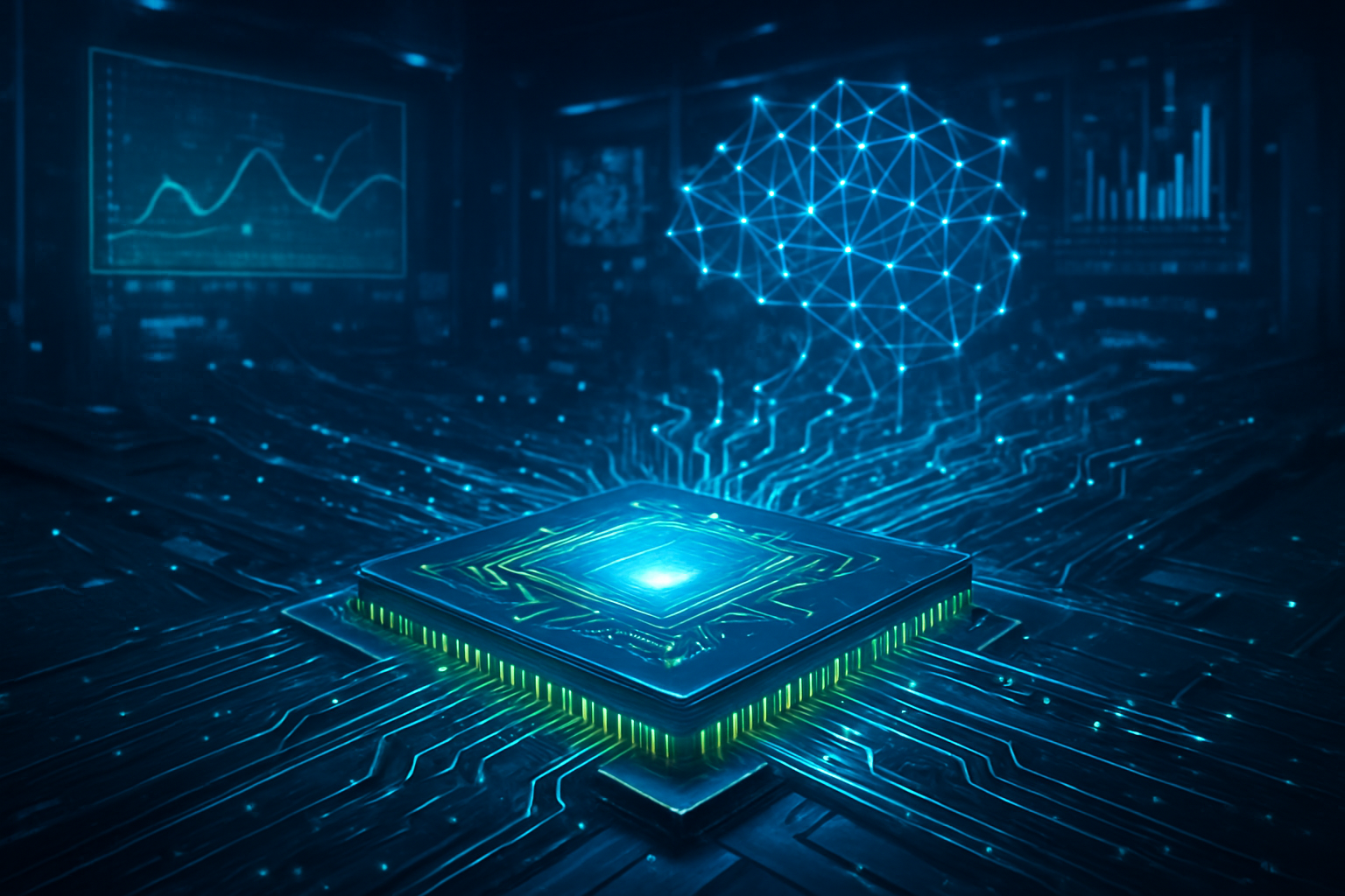
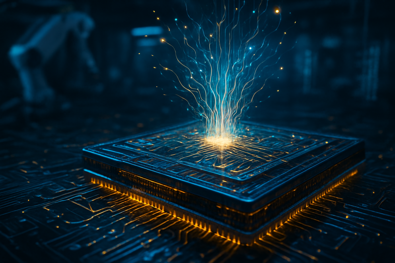
The technical landscape of 2025 was defined by the arrival of "System 2" thinking—a shift from the rapid, pattern-matching responses of early LLMs to deliberative, multi-step reasoning. Leading the charge was the release of OpenAI’s GPT-5.2 and Alphabet Inc.’s (NASDAQ: GOOGL) Gemini 3. These models introduced "Thinking Modes" that allow the AI to pause, verify intermediate steps, and self-correct before providing an answer. In benchmark testing, GPT-5.2 achieved a perfect 100% on the AIME 2025 (American Invitational Mathematics Examination), while Gemini 3 Pro demonstrated "Long-Horizon Reasoning," enabling it to manage multi-hour coding sessions without context drift.
Beyond pure reasoning, 2025 saw the rise of "Native Multimodality." Unlike previous versions that "stitched" together text and image encoders, Gemini 3 and OpenAI’s latest architectures process audio, video, and code within a single unified transformer stack. This has enabled "Native Video Understanding," where AI agents can watch a live video feed and interact with the physical world in real-time. This capability was further bolstered by the release of Meta Platforms, Inc.’s (NASDAQ: META) Llama 4, which brought high-performance, open-source reasoning to the developer community, challenging the dominance of closed-source labs.
The AI research community has reacted with a mix of awe and caution. While the leap in "vibe coding"—the ability to generate entire software applications from abstract sketches—has revolutionized development, experts point to the "DeepSeek R1" event in early 2025 as a wake-up call. This high-performance, low-cost model from China proved that massive compute isn't the only path to intelligence, forcing Western labs to pivot toward algorithmic efficiency. The resulting "efficiency wars" have driven down inference costs by 90% over the last twelve months, making high-level reasoning accessible to nearly every smartphone user.
Market Dominance and the $5 Trillion Milestone
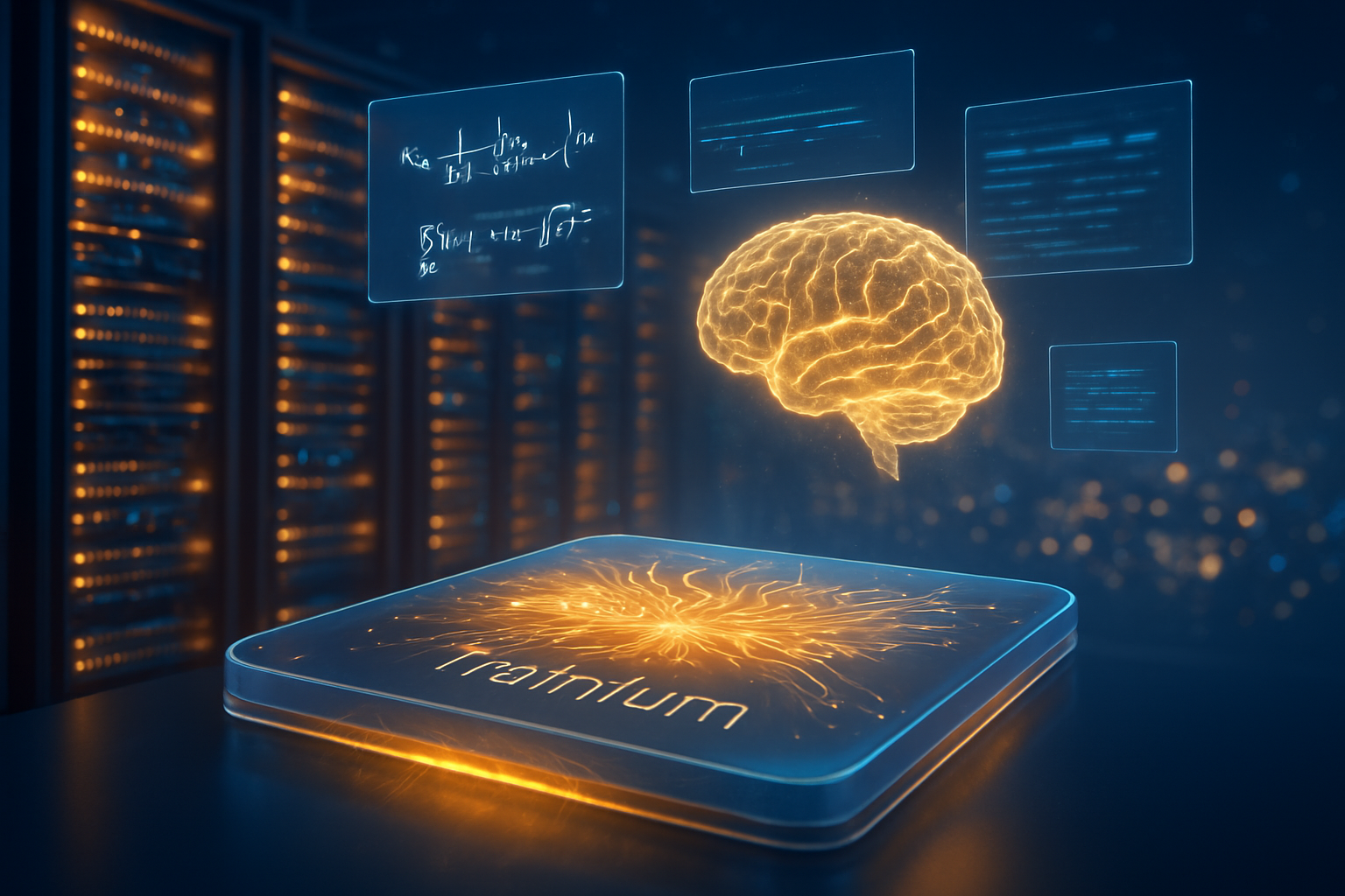
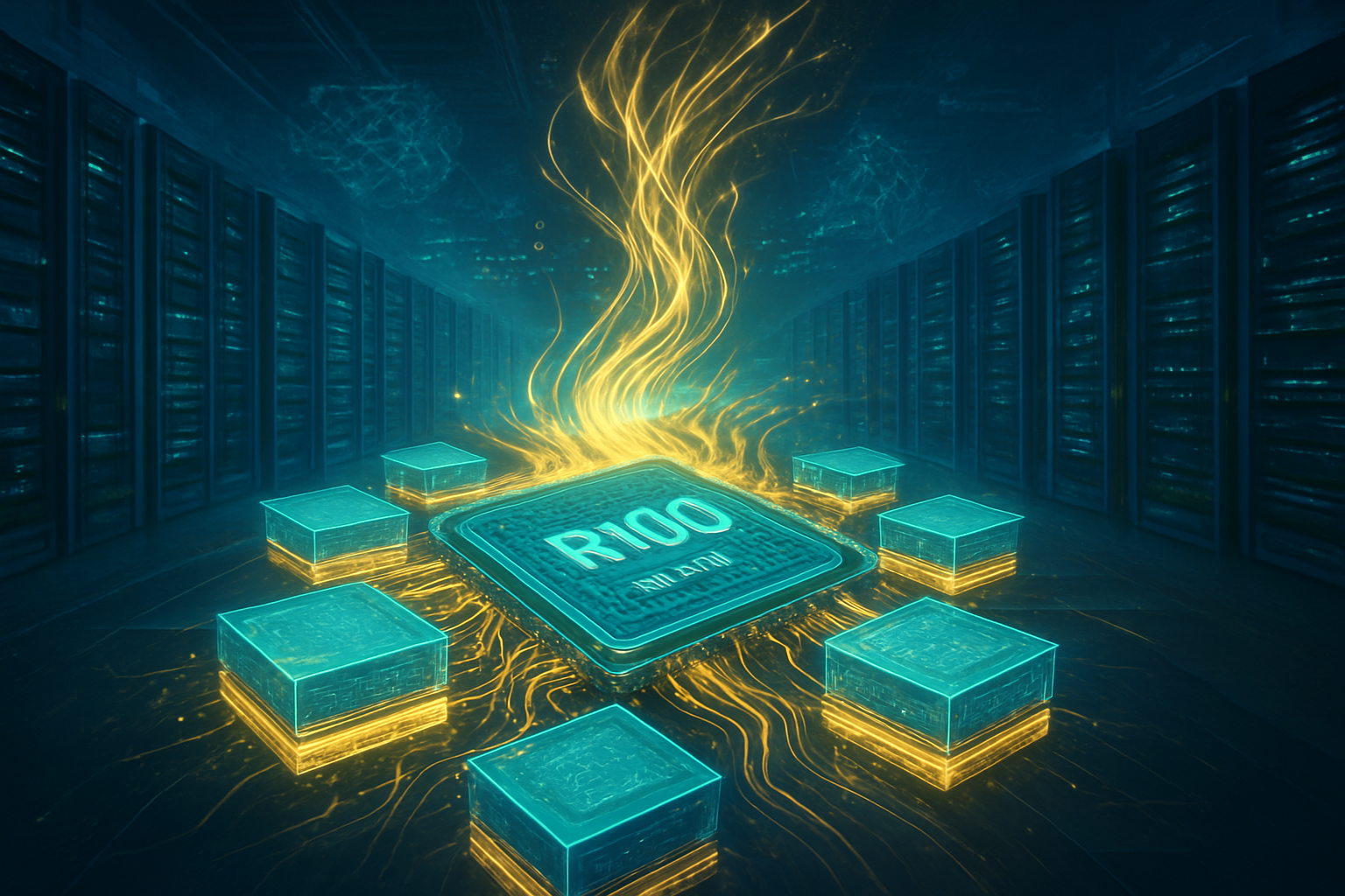
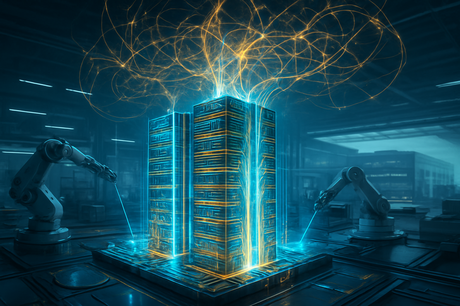
The business implications of these advancements have been nothing short of historic. In mid-2025, NVIDIA (NASDAQ: NVDA) became the world’s first $5 trillion company, fueled by insatiable demand for its Blackwell and subsequent "Rubin" GPU architectures. The company’s dominance is no longer just in hardware; its CUDA software stack has become the "operating system" for the AI era. Meanwhile, Advanced Micro Devices, Inc. (NASDAQ: AMD) has successfully carved out a significant share of the inference market, with its MI350 series becoming the preferred choice for cost-conscious enterprise deployments.
The competitive landscape shifted significantly with the formalization of the Stargate Project, a $500 billion joint venture between OpenAI, SoftBank Group Corp. (TYO: 9984), and Oracle Corporation (NYSE: ORCL). This initiative has decentralized the AI power structure, moving OpenAI away from its exclusive reliance on Microsoft Corporation (NASDAQ: MSFT). While Microsoft remains a critical partner, the Stargate Project’s massive 10-gigawatt data centers in Texas and Ohio have allowed OpenAI to pursue "Sovereign AI" infrastructure, designing custom silicon in partnership with Broadcom Inc. (NASDAQ: AVGO) to optimize its most compute-heavy models.
Startups have also found new life in the "Agentic Economy." Companies like World Labs and Anthropic have moved beyond general-purpose chatbots to "Specialist Agents" that handle everything from autonomous drug discovery to legal discovery. The disruption to existing SaaS products has been profound; legacy software providers that failed to integrate native reasoning into their core products have seen their valuations plummet as "AI-native" competitors automate entire departments that previously required dozens of human operators.
A Global Inflection Point: Geopolitics and Societal Risks
The recognition of AI as the "Person of the Year" also underscores its role as a primary instrument of geopolitical power. In 2025, AI became the center of a new "Cold War" between the U.S. and China, with both nations racing to secure the energy and silicon required for AGI. The "Stargate" initiative is viewed by many as a national security project as much as a commercial one. However, this race for dominance has raised significant environmental concerns, as the energy requirements for these "megaclusters" have forced a massive re-evaluation of global power grids and a renewed push for modular nuclear reactors.
Societally, the impact has been a "double-edged sword," as Time’s editorial noted. While AI-driven generative chemistry has reduced the timeline for validating new drug molecules from years to weeks, the labor market is feeling the strain. Reports in late 2025 suggest that up to 20% of roles in sectors like data entry, customer support, and basic legal research have faced significant disruption. Furthermore, the "worrying" side of AI was highlighted by high-profile lawsuits regarding "chatbot psychosis" and the proliferation of hyper-realistic deepfakes that have challenged the integrity of democratic processes worldwide.
Comparisons to previous milestones, such as the 1982 "Machine of the Year" (The Computer), are frequent. However, the 2025 recognition is distinct because it focuses on the Architects—emphasizing that while the technology is transformative, the ethical and strategic choices made by human leaders will determine its ultimate legacy. The "Godmother of AI," Fei-Fei Li, has used her platform to advocate for "Human-Centered AI," ensuring that the drive for intelligence does not outpace the development of safety frameworks and economic safety nets.
The Horizon: From Reasoning to Autonomy
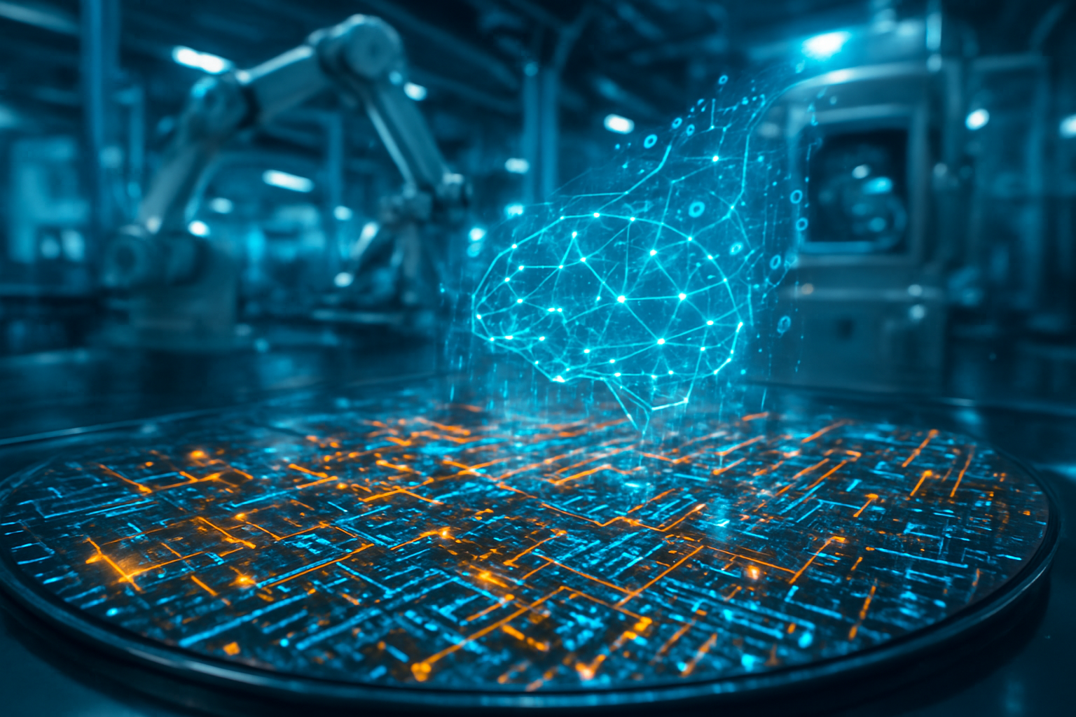
Looking ahead to 2026, experts predict the focus will shift from "Reasoning" to "Autonomy." We are entering the era of the "Agentic Web," where AI models will not just answer questions but will possess the agency to execute complex, multi-step tasks across the internet and physical world without human intervention. This includes everything from autonomous supply chain management to AI-driven scientific research labs that run 24/7.
The next major hurdle is the "Energy Wall." As the Stargate Project scales toward its 10-gigawatt goal, the industry must solve the cooling and power distribution challenges that come with such unprecedented density. Additionally, the development of "On-Device Reasoning"—bringing GPT-5 level intelligence to local hardware without relying on the cloud—is expected to be the next major battleground for companies like Apple Inc. (NASDAQ: AAPL) and Qualcomm Incorporated (NASDAQ: QCOM).
A Permanent Shift in the Human Story
The naming of "The Architects of AI" as the 2025 Person of the Year serves as a definitive marker for the end of the "Information Age" and the beginning of the "Intelligence Age." The key takeaway from 2025 is that AI is no longer a tool we use, but an environment we inhabit. It has become the invisible hand guiding global markets, scientific discovery, and personal productivity.
As we move into 2026, the world will be watching how these "Architects" handle the immense responsibility they have been granted. The significance of this development in AI history cannot be overstated; it is the year the technology became undeniable. Whether this leads to a "golden age" of productivity or a period of unprecedented social upheaval remains to be seen, but one thing is certain: the world of 2025 is fundamentally different from the one that preceded it.
This content is intended for informational purposes only and represents analysis of current AI developments.
TokenRing AI delivers enterprise-grade solutions for multi-agent AI workflow orchestration, AI-powered development tools, and seamless remote collaboration platforms.
For more information, visit https://www.tokenring.ai/.