Tag: Nvidia

  • The Great AI Rebound: Micron and Nvidia Lead ‘Supercycle’ Rally as Wall Street Rejects the Bubble Narrative

    The Great AI Rebound: Micron and Nvidia Lead ‘Supercycle’ Rally as Wall Street Rejects the Bubble Narrative

    The artificial intelligence sector experienced a thunderous resurgence on December 18, 2025, as a "blowout" earnings report from Micron Technology (NASDAQ: MU) effectively silenced skeptics and reignited a massive rally across the semiconductor landscape. After weeks of market anxiety characterized by a "Great Rotation" out of high-growth tech and into value sectors, the narrative has shifted back to the fundamental strength of AI infrastructure. Micron’s shares surged over 14% in mid-day trading, lifting the broader Nasdaq by 450 points and dragging industry titan Nvidia Corporation (NASDAQ: NVDA) up nearly 3% in its wake.

    This rally is more than just a momentary spike; it represents a fundamental validation of the AI "memory supercycle." With Micron announcing that its entire production capacity for High Bandwidth Memory (HBM) is already sold out through the end of 2026, the message to Wall Street is clear: the demand for AI hardware is not just sustained—it is accelerating. This development has provided a much-needed confidence boost to investors who feared that the massive capital expenditures of 2024 and early 2025 might lead to a glut of unused capacity. Instead, the industry is grappling with a structural supply crunch that is redefining the value of silicon.

    The Silicon Fuel: HBM4 and the Blackwell Ultra Era

    The technical catalyst for this rally lies in the rapid evolution of High Bandwidth Memory, the critical "fuel" that allows AI processors to function at peak efficiency. Micron confirmed during its earnings call that its next-generation HBM4 is on track for a high-yield production ramp in the second quarter of 2026. Built on a 1-beta process, Micron’s HBM4 is achieving data transfer speeds exceeding 11 Gbps. This represents a significant leap over the current HBM3E standard, offering the massive bandwidth necessary to feed the next generation of Large Language Models (LLMs) that are now approaching the 100-trillion parameter mark.

    Simultaneously, Nvidia is solidifying its dominance with the full-scale production of the Blackwell Ultra GB300 series. The GB300 offers a 1.5x performance boost in AI inferencing over the original Blackwell architecture, largely due to its integration of up to 288GB of HBM3E and early HBM4E samples. This "Ultra" cycle is a strategic pivot by Nvidia to maintain a relentless one-year release cadence, ensuring that competitors like Advanced Micro Devices (NASDAQ: AMD) are constantly chasing a moving target. Industry experts have noted that the Blackwell Ultra’s ability to handle massive context windows for real-time video and multimodal AI is a direct result of this tighter integration between logic and memory.

    Initial reactions from the AI research community have been overwhelmingly positive, particularly regarding the thermal efficiency of the new 12- and 16-layer HBM stacks. Unlike previous iterations that struggled with heat dissipation at high clock speeds, the 2025-era HBM4 utilizes advanced molded underfill (MR-MUF) techniques and hybrid bonding. This allows for denser stacking without the thermal throttling that plagued early AI accelerators, enabling the 15-exaflop rack-scale systems that are currently being deployed by cloud giants.

    A Three-Way War for Memory Supremacy

    The current rally has also clarified the competitive landscape among the "Big Three" memory makers. While SK Hynix (KRX: 000660) remains the market leader with a 55% share of the HBM market, Micron has successfully leapfrogged Samsung Electronics (KRX: 000660) to secure the number two spot in HBM bit shipments. Micron’s strategic advantage in late 2025 stems from its position as the primary U.S.-based supplier, making it a preferred partner for sovereign AI projects and domestic cloud providers looking to de-risk their supply chains.

    However, Samsung is mounting a significant comeback. After trailing in the HBM3E race, Samsung has reportedly entered the final qualification stage for its "Custom HBM" for Nvidia’s upcoming Vera Rubin platform. Samsung’s unique "one-stop-shop" strategy—manufacturing both the HBM layers and the logic die in-house—allows it to offer integrated solutions that its competitors cannot. This competition is driving a massive surge in profitability; for the first time in history, memory makers are seeing gross margins approaching 68%, a figure typically reserved for high-end logic designers.

    For the tech giants, this supply-constrained environment has created a strategic moat. Companies like Meta (NASDAQ: META) and Amazon (NASDAQ: AMZN) have moved to secure multi-year supply agreements, effectively "pre-buying" the next two years of AI capacity. This has left smaller AI startups and tier-2 cloud providers in a difficult position, as they must now compete for a dwindling pool of unallocated chips or turn to secondary markets where prices for standard DDR5 DRAM have jumped by over 420% due to wafer capacity being diverted to HBM.

    The Structural Shift: From Commodity to Strategic Infrastructure

    The broader significance of this rally lies in the transformation of the semiconductor industry. Historically, the memory market was a boom-and-bust commodity business. In late 2025, however, memory is being treated as "strategic infrastructure." The "memory wall"—the bottleneck where processor speed outpaces data delivery—has become the primary challenge for AI development. As a result, HBM is no longer just a component; it is the gatekeeper of AI performance.

    This shift has profound implications for the global economy. The HBM Total Addressable Market (TAM) is now projected to hit $100 billion by 2028, a milestone reached two years earlier than most analysts predicted in 2024. This rapid expansion suggests that the "AI trade" is not a speculative bubble but a fundamental re-architecting of global computing power. Comparisons to the 1990s internet boom are becoming less frequent, replaced by parallels to the industrialization of electricity or the build-out of the interstate highway system.

    Potential concerns remain, particularly regarding the concentration of supply in the hands of three companies and the geopolitical risks associated with manufacturing in East Asia. However, the aggressive expansion of Micron’s domestic manufacturing capabilities and Samsung’s diversification of packaging sites have partially mitigated these fears. The market's reaction on December 18 indicates that, for now, the appetite for growth far outweighs the fear of overextension.

    The Road to Rubin and the 15-Exaflop Future

    Looking ahead, the roadmap for 2026 and 2027 is already coming into focus. Nvidia’s Vera Rubin architecture, slated for a late 2026 release, is expected to provide a 3x performance leap over Blackwell. Powered by new R100 GPUs and custom ARM-based CPUs, Rubin will be the first platform designed from the ground up for HBM4. Experts predict that the transition to Rubin will mark the beginning of the "Physical AI" era, where models are large enough and fast enough to power sophisticated humanoid robotics and autonomous industrial fleets in real-time.

    AMD is also preparing its response with the MI400 series, which promises a staggering 432GB of HBM4 per GPU. By positioning itself as the leader in memory capacity, AMD is targeting the massive LLM inference market, where the ability to fit a model entirely on-chip is more critical than raw compute cycles. The challenge for both companies will be securing enough 3nm and 2nm wafer capacity from TSMC to meet the insatiable demand.

    In the near term, the industry will focus on the "Sovereign AI" trend, as nation-states begin to build out their own independent AI clusters. This will likely lead to a secondary "mini-cycle" of demand that is decoupled from the spending of U.S. hyperscalers, providing a safety net for chipmakers if domestic commercial demand ever starts to cool.

    Conclusion: The AI Trade is Back for the Long Haul

    The mid-december rally of 2025 has served as a definitive turning point for the tech sector. By delivering record-breaking earnings and a "sold-out" outlook, Micron has provided the empirical evidence needed to sustain the AI bull market. The synergy between Micron’s memory breakthroughs and Nvidia’s relentless architectural innovation has created a feedback loop that continues to defy traditional market cycles.

    This development is a landmark in AI history, marking the moment when the industry moved past the "proof of concept" phase and into a period of mature, structural growth. The AI trade is no longer about the potential of what might happen; it is about the reality of what is being built. Investors should watch closely for the first HBM4 qualification results in early 2026 and any shifts in capital expenditure guidance from the major cloud providers. For now, the "AI Chip Rally" suggests that the foundation of the digital future is being laid in silicon, and the builders are working at full capacity.


    This content is intended for informational purposes only and represents analysis of current AI developments.

    TokenRing AI delivers enterprise-grade solutions for multi-agent AI workflow orchestration, AI-powered development tools, and seamless remote collaboration platforms.
    For more information, visit https://www.tokenring.ai/.


    Disclaimer: The dates and events described in this article are based on the user-provided context of December 18, 2025.

  • The Defensive Frontier: New ETFs Signal a Massive Shift Toward AI Security and Embodied Robotics

    The Defensive Frontier: New ETFs Signal a Massive Shift Toward AI Security and Embodied Robotics

    As 2025 draws to a close, the artificial intelligence investment landscape has undergone a profound transformation. The "generative hype" of previous years has matured into a disciplined focus on the infrastructure of trust and the physical manifestation of intelligence. This shift is most visible in the surge of specialized Exchange-Traded Funds (ETFs) targeting AI Security and Humanoid Robotics, which have become the dual engines of the sector's growth. Investors are no longer just betting on models that can write; they are betting on systems that can move and, more importantly, systems that cannot be compromised.

    The immediate significance of this development lies in the realization that enterprise AI adoption has hit a "security ceiling." While the global AI market is projected to reach $243.72 billion by the end of 2025, a staggering 94% of organizations still lack an advanced AI security strategy. This gap has turned AI security from a niche technical requirement into a multi-billion dollar investment theme, driving a new class of financial products designed to capture the "Second Wave" of the AI revolution.

    The Rise of "Physical AI" and Secure Architectures

    The technical narrative of 2025 is dominated by the emergence of "Embodied AI"—intelligence that interacts with the physical world. This has been codified by the launch of groundbreaking investment vehicles like the KraneShares Global Humanoid and Embodied Intelligence Index ETF (KOID). Unlike earlier robotics funds that focused on static industrial arms, KOID and the Themes Humanoid Robotics ETF (BOTT) specifically target the supply chain for bipedal and dexterous robots. These ETFs represent a bet on the "Physical AI" foundation models developed by companies like NVIDIA (NASDAQ: NVDA), whose Cosmos and Omniverse platforms are now providing the "digital twins" necessary to train robots in virtual environments before they ever touch a factory floor.

    On the security front, the industry is grappling with technical threats that were theoretical just two years ago. "Prompt Injection" has become the modern equivalent of the SQL injection, where malicious users bypass a model's safety guardrails to extract sensitive data. Even more insidious is "Data Poisoning," a "slow-kill" attack where adversaries corrupt a model's training set to manipulate its logic months after deployment. To combat this, a new sub-sector called AI Security Posture Management (AI-SPM) has emerged. This technology differs from traditional cybersecurity by focusing on the "weights and biases" of the models themselves, rather than just the networks they run on.

    Industry experts note that these technical challenges are the primary reason for the rebranding of major funds. For instance, BlackRock (NYSE: BLK) recently pivoted its iShares Future AI and Tech ETF (ARTY) to focus specifically on the "full value chain" of secure deployment. The consensus among researchers is that the "Wild West" era of AI experimentation is over; the era of the "Fortified Model" has begun.

    Market Positioning: The Consolidation of AI Defense

    The shift toward AI security has created a massive strategic advantage for "platform" companies that can offer integrated defense suites. Palo Alto Networks (NASDAQ: PANW) has emerged as a leader in this space through its "platformization" strategy, recently punctuated by its acquisition of Protect AI to secure the entire machine learning lifecycle. By consolidating AI security tools into a single pane of glass, PANW is positioning itself as the indispensable gatekeeper for enterprise AI. Similarly, CrowdStrike (NASDAQ: CRWD) has leveraged its Falcon platform to provide real-time AI threat hunting, preventing prompt injections at the user level before they can reach the core model.

    In the robotics sector, the competitive implications are equally high-stakes. Figure AI, which reached a $39 billion valuation in 2025, has successfully integrated its Figure 02 humanoid into BMW (OTC: BMWYY) manufacturing facilities. This move has forced major tech giants to accelerate their own physical AI timelines. Tesla (NASDAQ: TSLA) has responded by deploying thousands of its Optimus Gen 2 robots within its own Gigafactories, aiming to prove commercial viability ahead of a broader enterprise launch slated for 2026.

    This market positioning reflects a "winner-takes-most" dynamic. Companies like Palantir (NASDAQ: PLTR), with its AI Platform (AIP), are benefiting from a flight to "sovereign AI"—environments where data security and model integrity are guaranteed. For tech giants, the strategic advantage no longer comes from having the largest model, but from having the most secure and physically capable ecosystem.

    Wider Significance: The Infrastructure of Trust

    The rise of AI security and robotics ETFs fits into a broader trend of "De-risking AI." In the early 2020s, the focus was on capability; in 2025, the focus is on reliability. This transition is reminiscent of the early days of the internet, where e-commerce could not flourish until SSL encryption and secure payment gateways became standard. AI security is the "SSL moment" for the generative era. Without it, the massive investments made by Fortune 500 companies in Large Language Models (LLMs) remain a liability rather than an asset.

    However, this evolution brings potential concerns. The concentration of security and robotics power in a handful of "platform" companies could lead to significant market gatekeeping. Furthermore, as AI becomes "embodied" in humanoid forms, the ethical and safety implications move from the digital realm to the physical one. A "hacked" chatbot is a PR disaster; a "hacked" humanoid robot in a warehouse is a physical threat. This has led to a surge in "AI Red Teaming"—where companies hire hackers to find vulnerabilities in their physical and digital AI systems—as a mandatory part of corporate governance.

    Comparatively, this milestone exceeds previous AI breakthroughs like AlphaGo or the initial launch of ChatGPT. Those were demonstrations of potential; the current shift toward secure, physical AI is a demonstration of utility. We are moving from AI as a "consultant" to AI as a "worker" and a "guardian."

    Future Developments: Toward General Purpose Autonomy

    Looking ahead to 2026, experts predict the "scaling law" for robotics will mirror the scaling laws we saw for LLMs. As more data is gathered from physical interactions, humanoid robots will move from highly scripted tasks in controlled environments to "general-purpose" roles in unstructured settings like hospitals and retail stores. The near-term development to watch is the integration of "Vision-Language-Action" (VLA) models, which allow robots to understand verbal instructions and translate them into complex physical maneuvers in real-time.

    Challenges remain, particularly in the realm of "Model Inversion" defense. Researchers are still struggling to find a foolproof way to prevent attackers from reverse-engineering training data from a model's outputs. Addressing this will be critical for industries like healthcare and finance, where data privacy is legally mandated. We expect to see a new wave of "Privacy-Preserving AI" startups that use synthetic data and homomorphic encryption to train models without ever "seeing" the underlying sensitive information.

    Conclusion: The New Standard for Intelligence

    The rise of AI Security and Robotics ETFs marks a turning point in the history of technology. It signifies the end of the experimental phase of artificial intelligence and the beginning of its integration into the bedrock of global industry. The key takeaway for 2025 is that intelligence is no longer enough; for AI to be truly transformative, it must be both secure and capable of physical labor.

    The significance of this development cannot be overstated. By solving the security bottleneck, the industry is clearing the path for the next trillion dollars of enterprise value. In the coming weeks and months, investors should closely monitor the performance of "embodied AI" pilots in the automotive and logistics sectors, as well as the adoption rates of AI-SPM platforms among the Global 2000. The frontier has moved: the most valuable AI is no longer the one that talks the best, but the one that works the safest.


    This content is intended for informational purposes only and represents analysis of current AI developments.

    TokenRing AI delivers enterprise-grade solutions for multi-agent AI workflow orchestration, AI-powered development tools, and seamless remote collaboration platforms.
    For more information, visit https://www.tokenring.ai/.

  • NOAA Launches Project EAGLE: The AI Revolution in Global Weather Forecasting

    NOAA Launches Project EAGLE: The AI Revolution in Global Weather Forecasting

    On December 17, 2025, the National Oceanic and Atmospheric Administration (NOAA) ushered in a new era of meteorological science by officially operationalizing its first suite of AI-driven global weather models. This milestone, part of an initiative dubbed Project EAGLE, represents the most significant shift in American weather forecasting since the introduction of satellite data. By moving from purely physics-based simulations to a sophisticated hybrid AI-physics framework, NOAA is now delivering forecasts that are not only more accurate but are produced at a fraction of the computational cost of traditional methods.

    The immediate significance of this development cannot be overstated. For decades, the Global Forecast System (GFS) has been the backbone of American weather prediction, relying on supercomputers to solve complex fluid dynamics equations. The transition to the new Artificial Intelligence Global Forecast System (AIGFS) and its ensemble counterparts means that 16-day global forecasts, which previously required hours of supercomputing time, can now be generated in roughly 40 minutes. This speed allows for more frequent updates and more granular data, providing emergency responders and the public with critical lead time during rapidly evolving extreme weather events.

    Technical Breakthroughs: AIGFS, AIGEFS, and the Hybrid Edge

    The technical core of Project EAGLE consists of three primary systems: the AIGFS v1.0, the AIGEFS v1.0 (ensemble system), and the HGEFS v1.0 (Hybrid Global Ensemble Forecast System). The AIGFS is a deterministic model based on a specialized version of GraphCast, an AI architecture originally developed by Google DeepMind, a subsidiary of Alphabet Inc. (NASDAQ: GOOGL). While the base architecture is shared, NOAA researchers retrained the model using the agency’s proprietary Global Data Assimilation System (GDAS) data, tailoring the AI to better handle the nuances of North American geography and global atmospheric patterns.

    The most impressive technical feat is the 99.7% reduction in computational resources required for the AIGFS compared to the traditional physics-based GFS. While the old system required massive clusters of CPUs to simulate atmospheric physics, the AI models leverage the parallel processing power of modern GPUs. Furthermore, the HGEFS—a "grand ensemble" of 62 members—combines 31 traditional physics-based members with 31 AI-driven members. This hybrid approach mitigates the "black box" nature of AI by grounding its statistical predictions in established physical laws, resulting in a system that extended forecast skill by an additional 18 to 24 hours in initial testing.

    Initial reactions from the AI research community have been overwhelmingly positive, though cautious. Experts at the Earth Prediction Innovation Center (EPIC) noted that while the AIGFS significantly reduces errors in tropical cyclone track forecasting, early versions still show a slight degradation in predicting hurricane intensity compared to traditional models. This trade-off—better path prediction but slightly less precision in wind speed—is a primary reason why NOAA has opted for a hybrid operational strategy rather than a total replacement of physics-based systems.

    The Silicon Race for the Atmosphere: Industry Impact

    The operationalization of these models cements the status of tech giants as essential partners in national infrastructure. Alphabet Inc. (NASDAQ: GOOGL) stands as a primary beneficiary, with its DeepMind architecture now serving as the literal engine for U.S. weather forecasts. This deployment validates the real-world utility of GraphCast beyond academic benchmarks. Meanwhile, Microsoft Corp. (NASDAQ: MSFT) has secured its position through a Cooperative Research and Development Agreement (CRADA), hosting NOAA's massive data archives on its Azure cloud platform and piloting the EPIC projects that made Project EAGLE possible.

    The hardware side of this revolution is dominated by NVIDIA Corp. (NASDAQ: NVDA). The shift from CPU-heavy physics models to GPU-accelerated AI models has triggered a massive re-allocation of NOAA’s hardware budget toward NVIDIA’s H200 and Blackwell architectures. NVIDIA is also collaborating with NOAA on "Earth-2," a digital twin of the planet that uses models like CorrDiff to predict localized supercell storms and tornadoes at a 3km resolution—precision that was computationally impossible just three years ago.

    This development creates a competitive pressure on other global meteorological agencies. While the European Centre for Medium-Range Weather Forecasts (ECMWF) launched its own AI system, AIFS, in February 2025, NOAA’s hybrid ensemble approach is now being hailed as the more robust solution for handling extreme outliers. This "weather arms race" is driving a surge in startups focused on AI-driven climate risk assessment, as they can now ingest NOAA’s high-speed AI data to provide hyper-local forecasts for insurance and energy companies.

    A Milestone in the Broader AI Landscape

    Project EAGLE fits into a broader trend of "Scientific AI," where machine learning is used to accelerate the discovery and simulation of physical processes. Much like AlphaFold revolutionized biology, the AIGFS is revolutionizing atmospheric science. This represents a move away from "Generative AI" that creates text or images, toward "Predictive AI" that manages real-world physical risks. The transition marks a maturing of the AI field, proving that these models can handle the high-stakes, zero-failure environment of national security and public safety.

    However, the shift is not without concerns. Critics point out that AI models are trained on historical data, which may not accurately reflect the "new normal" of a rapidly changing climate. If the atmosphere behaves in ways it never has before, an AI trained on the last 40 years of data might struggle to predict unprecedented "black swan" weather events. Furthermore, the reliance on proprietary architectures from companies like Alphabet and Microsoft raises questions about the long-term sovereignty of public weather data.

    Despite these concerns, the efficiency gains are undeniable. The ability to run hundreds of forecast scenarios simultaneously allows meteorologists to quantify uncertainty in ways that were previously a luxury. In an era of increasing climate volatility, the reduced computational cost means that even smaller nations can eventually run high-quality global models, potentially democratizing weather intelligence that was once the sole domain of wealthy nations with supercomputers.

    The Horizon: 3km Resolution and Beyond

    Looking ahead, the next phase of NOAA’s AI integration will focus on "downscaling." While the current AIGFS provides global coverage, the near-term goal is to implement AI models that can predict localized weather—such as individual thunderstorms or urban heat islands—at a 1-kilometer to 3-kilometer resolution. This will be a game-changer for the aviation and agriculture industries, where micro-climates can dictate operational success or failure.

    Experts predict that within the next two years, we will see the emergence of "Continuous Data Assimilation," where AI models are updated in real-time as new satellite and sensor data arrives, rather than waiting for the traditional six-hour forecast cycles. The challenge remains in refining the AI's ability to predict extreme intensity and rare atmospheric phenomena. Addressing the "intensity gap" in hurricane forecasting will be the primary focus of the AIGFS v2.0, expected in late 2026.

    Conclusion: A New Era of Certainty

    The launch of Project EAGLE and the operationalization of the AIGFS suite mark a definitive turning point in the history of meteorology. By successfully blending the statistical power of AI with the foundational reliability of physics, NOAA has created a forecasting framework that is faster, cheaper, and more accurate than its predecessors. This is not just a technical upgrade; it is a fundamental reimagining of how we interact with the planet's atmosphere.

    As we look toward 2026, the success of this rollout will be measured by its performance during the upcoming spring tornado season and the Atlantic hurricane season. The significance of this development in AI history is clear: it is the moment AI moved from being a digital assistant to a critical guardian of public safety. For the tech industry, it underscores the vital importance of the partnership between public institutions and private innovators. The world is watching to see how this "new paradigm" holds up when the clouds begin to gather.


    This content is intended for informational purposes only and represents analysis of current AI developments.

    TokenRing AI delivers enterprise-grade solutions for multi-agent AI workflow orchestration, AI-powered development tools, and seamless remote collaboration platforms.
    For more information, visit https://www.tokenring.ai/.

  • Dismantling the Memory Wall: How HBM4 and Processing-in-Memory Are Re-Architecting the AI Era

    Dismantling the Memory Wall: How HBM4 and Processing-in-Memory Are Re-Architecting the AI Era

    As the artificial intelligence industry closes out 2025, the narrative of "bigger is better" regarding compute power has shifted toward a more fundamental physical constraint: the "Memory Wall." For years, the raw processing speed of GPUs has outpaced the rate at which data can be moved from memory to the processor, leaving the world’s most advanced AI chips idling for significant portions of their operation. However, a series of breakthroughs in late 2025—headlined by the mass production of HBM4 and the commercial debut of Processing-in-Memory (PIM) architectures—marks a pivotal moment where the industry is finally beginning to dismantle this bottleneck.

    The immediate significance of these developments cannot be overstated. As Large Language Models (LLMs) like GPT-5 and Llama 4 push toward multi-trillion parameter scales, the cost and energy required to move data between components have become the primary limiters of AI performance. By integrating compute capabilities directly into the memory stack and doubling the data bus width, the industry is moving from a "compute-centric" to a "memory-centric" architecture. This shift is expected to reduce the energy consumption of AI inference by up to 70%, effectively extending the life of current data center power grids while enabling the next generation of "Agentic AI" that requires massive, persistent memory contexts.

    The Technical Breakthrough: HBM4 and the 2,048-Bit Leap

    The technical cornerstone of this evolution is High Bandwidth Memory 4 (HBM4). Unlike its predecessor, HBM3E, which utilized a 1,024-bit interface, HBM4 doubles the width of the data highway to 2,048 bits. This change, showcased prominently at the Supercomputing Conference (SC25) in November, allows for bandwidths exceeding 2 TB/s per stack. SK Hynix (KRX: 000660) led the charge this year by demonstrating the world's first 12-layer HBM4 stacks, which utilize a base logic die manufactured on advanced foundry processes to manage the massive data flow.

    Beyond raw bandwidth, the emergence of Processing-in-Memory (PIM) represents a radical departure from the traditional Von Neumann architecture, where the CPU/GPU and memory are separate entities. Technologies like SK Hynix's AiMX and Samsung (KRX: 005930) Mach-1 are now embedding AI processing units directly into the memory chips themselves. This allows the memory to handle specific tasks—such as the "Attention" mechanisms in LLMs or Key-Value (KV) cache management—without ever sending the data back to the main GPU. By performing these operations "in-place," PIM chips eliminate the latency and energy overhead of the data bus, which has historically been the "wall" preventing real-time performance in long-context AI applications.

    Initial reactions from the research community have been overwhelmingly positive. Dr. Elena Rossi, a senior hardware analyst, noted at SC25 that "we are finally seeing the end of the 'dark silicon' era where GPUs sat waiting for data. The integration of a 4nm logic die at the base of the HBM4 stack allows for a level of customization we’ve never seen, essentially turning the memory into a co-processor." This "Custom HBM" trend allows companies like NVIDIA (NASDAQ: NVDA) to co-design the memory logic with foundries like TSMC (NYSE: TSM), ensuring that the memory architecture is perfectly tuned for the specific mathematical kernels used in modern transformer models.

    The Competitive Landscape: NVIDIA’s Rubin and the Memory Giants

    The shift toward memory-centric computing is redrawing the competitive map for tech giants. NVIDIA (NASDAQ: NVDA) remains the dominant force, but its strategy has pivoted toward a yearly release cadence to keep pace with memory advancements. The recently detailed "Rubin" R100 GPU architecture, slated for full mass production in early 2026, is designed from the ground up to leverage HBM4. With eight HBM4 stacks providing a staggering 13 TB/s of system bandwidth, NVIDIA is positioning itself not just as a chip maker, but as a system architect that controls the entire data path via its NVLink 7 interconnects.

    Meanwhile, the "Memory War" between SK Hynix, Samsung, and Micron (NASDAQ: MU) has reached a fever pitch. Samsung, which trailed in the HBM3E cycle, has signaled a massive comeback in December 2025 by reporting 90% yields on its HBM4 logic dies. Samsung is also pushing the "AI at the edge" frontier with its SOCAMM2 and LPDDR6-PIM standards, reportedly in collaboration with Apple (NASDAQ: AAPL) to bring high-performance AI memory to future mobile devices. Micron, while slightly behind in the HBM4 ramp, announced that its 2026 supply is already sold out, underscoring the insatiable demand for high-speed memory across the industry.

    This development is also a boon for specialized AI startups and cloud providers. The introduction of CXL 3.2 (Compute Express Link) allows for "Memory Pooling," where multiple GPUs can share a massive bank of external memory. This effectively disrupts the current limitation where an AI model's size is capped by the VRAM of a single GPU. Startups focusing on inference-dedicated ASICs are now using PIM to offer "LLM-in-a-box" solutions that provide the performance of a multi-million dollar cluster at a fraction of the power and cost, challenging the dominance of traditional hyperscale data centers.

    Wider Significance: Sustainability and the Rise of Agentic AI

    The broader implications of dismantling the Memory Wall extend far beyond technical benchmarks. Perhaps the most critical impact is on sustainability. In 2024, the energy consumption of AI data centers was a growing global concern. By late 2025, the 10x to 20x reduction in "Energy per Token" enabled by PIM and HBM4 has provided a much-needed reprieve. This efficiency gain allows for the "democratization" of AI, as smaller, more efficient hardware can now run models that previously required massive power-hungry clusters.

    Furthermore, solving the memory bottleneck is the primary enabler of "Agentic AI"—systems capable of long-term reasoning and multi-step task execution. Agents require a "working memory" (the KV-cache) that can span millions of tokens. Previously, the Memory Wall made maintaining such a large context window prohibitively slow and expensive. With HBM4 and CXL-based memory pooling, AI agents can now "remember" hours of conversation or thousands of pages of documentation in real-time, moving AI from a simple chatbot interface to a truly autonomous digital colleague.

    However, this breakthrough also brings concerns. The concentration of the HBM4 supply chain in the hands of three major players (SK Hynix, Samsung, and Micron) and one major foundry (TSMC) creates a significant geopolitical and economic choke point. Furthermore, as hardware becomes more efficient, the "Jevons Paradox" may take hold: the increased efficiency could lead to even greater total energy consumption as the sheer volume of AI deployment explodes across every sector of the economy.

    The Road Ahead: 3D Stacking and Optical Interconnects

    Looking toward 2026 and beyond, the industry is already eyeing the next set of hurdles. While HBM4 and PIM have provided a temporary bridge over the Memory Wall, the long-term solution likely involves true 3D integration. Experts predict that the next major milestone will be "bumpless" bonding, where memory and logic are stacked directly on top of each other with such high density that the distinction between the two virtually disappears.

    We are also seeing the early stages of optical interconnects moving from the rack-to-rack level down to the chip-to-chip level. Companies are experimenting with using light instead of electricity to move data between the memory and the processor, which could theoretically provide infinite bandwidth with zero heat generation. In the near term, expect to see the "Custom HBM" trend accelerate, with AI labs like OpenAI and Meta (NASDAQ: META) designing their own proprietary memory logic to gain a competitive edge in model performance.

    Challenges remain, particularly in the software layer. Current programming models like CUDA are optimized for moving data to the compute; re-writing these frameworks to support "computing in the memory" is a monumental task that the industry is only beginning to address. Nevertheless, the consensus among experts is clear: the architecture of the next decade of AI will be defined not by how fast we can calculate, but by how intelligently we can store and move data.

    A New Foundation for Intelligence

    The dismantling of the Memory Wall marks a transition from the "Brute Force" era of AI to the "Architectural Refinement" era. By doubling bandwidth with HBM4 and bringing compute to the data through PIM, the industry has successfully bypassed a physical limit that many feared would stall AI progress by 2025. This achievement is as significant as the transition from CPUs to GPUs was a decade ago, providing the physical foundation necessary for the next leap in machine intelligence.

    As we move into 2026, the success of these technologies will be measured by their deployment in the wild. Watch for the first HBM4-powered "Rubin" systems to hit the market and for the integration of PIM into consumer devices, which will signal the arrival of truly capable on-device AI. The Memory Wall has not been completely demolished, but for the first time in the history of modern computing, we have found a way to build a door through it.


    This content is intended for informational purposes only and represents analysis of current AI developments.

    TokenRing AI delivers enterprise-grade solutions for multi-agent AI workflow orchestration, AI-powered development tools, and seamless remote collaboration platforms.
    For more information, visit https://www.tokenring.ai/.

  • Silicon Zenith: How a Macroeconomic Thaw and the 2nm Revolution Ignited the Greatest Semiconductor Rally in History

    Silicon Zenith: How a Macroeconomic Thaw and the 2nm Revolution Ignited the Greatest Semiconductor Rally in History

    As of December 18, 2025, the semiconductor industry is basking in the glow of a historic year, marked by a "perfect storm" of cooling inflation and monumental technological breakthroughs. This convergence has propelled the Philadelphia Semiconductor Index to all-time highs, driven by a global race to build the infrastructure for the next generation of artificial intelligence. While a mid-December "valuation reset" has introduced some volatility, the underlying fundamentals of the sector have never looked more robust, as the world transitions from simple generative models to complex, autonomous "Agentic AI."

    The rally is the result of a rare alignment between macroeconomic stability and a leap in manufacturing capabilities. With the Federal Reserve aggressively cutting interest rates as inflation settled into a 2.1% to 2.7% range, capital has flowed back into high-growth tech stocks. Simultaneously, the industry reached a long-awaited milestone: the move to 2-nanometer (2nm) production. This technical achievement, combined with NVIDIA’s (NASDAQ:NVDA) unveiling of its Rubin architecture, has fundamentally shifted expectations for AI performance, making the "AI bubble" talk of 2024 feel like a distant memory.

    The 2nm Era and the Rubin Revolution

    The technical backbone of this rally is the successful transition to volume production of 2nm chips. Taiwan Semiconductor Manufacturing Company (NYSE:TSM) officially moved its N2 process into high-volume manufacturing in the second half of 2025, reporting "promising" initial yields that exceeded analyst expectations. This move represents more than just a shrink in size; it introduces Gate-All-Around (GAA) transistor architecture at scale, providing a 15% speed improvement and a 30% reduction in power consumption compared to the previous 3nm nodes. This efficiency is critical for data centers that are currently straining global power grids.

    Parallel to this manufacturing feat is the arrival of NVIDIA’s Rubin R100 GPU architecture, which entered its sampling phase in late 2025. Unlike the Blackwell generation that preceded it, Rubin utilizes a sophisticated multi-die design enabled by TSMC’s CoWoS-L packaging. The Rubin platform features the new "Vera" CPU—an 88-core Arm-based processor—and integrates HBM4 memory, providing a staggering 13.5 TB/s of bandwidth. Industry experts note that Rubin is designed specifically for "World Models" and large-scale physical simulations, offering a 2.5x performance leap that justifies the massive capital expenditures seen throughout the year.

    Furthermore, the adoption of High-NA (Numerical Aperture) EUV lithography has finally reached the factory floor. ASML (NASDAQ:ASML) began shipping its Twinscan EXE:5200B machines in volume this December. Intel (NASDAQ:INTC) has been a primary beneficiary here, completing validation for its 14A (1.4nm) process using these machines. This technological "arms race" has created a hardware environment where the physical limits of silicon are being pushed further than ever, providing the necessary compute for the increasingly complex AI agents currently being deployed across the enterprise sector.

    Market Dominance and the Battle for the AI Data Center

    The financial impact of these breakthroughs has been nothing short of transformative for the industry’s leaders. NVIDIA (NASDAQ:NVDA) briefly touched a $5 trillion market capitalization in early December, maintaining a dominant 90% share of the advanced AI chip market. Despite a 3.8% profit-taking dip on December 18, the company’s shift from selling individual accelerators to providing "AI Factories"—rack-scale systems like the NVL144—has solidified its position as the essential utility of the AI age.

    AMD (NASDAQ:AMD) has emerged as a formidable challenger in 2025, with its stock up 72% year-to-date. By aggressively transitioning its upcoming Zen 6 architecture to 2nm and capturing 27.8% of the server CPU market, AMD has proven it can compete on both price and performance. Meanwhile, Broadcom (NASDAQ:AVGO) reported a 74% surge in AI-related revenue in its Q4 earnings, driven by the massive demand for custom AI ASICs from hyperscalers like Google and Meta. While Broadcom’s stock faced a mid-month tumble due to narrowing margins on custom silicon, its role in the networking fabric of AI data centers remains undisputed.

    However, the rally has not been without its casualties. The "monetization gap" remains a concern for some investors. Oracle (NYSE:ORCL), for instance, faced a $10 billion financing setback for its massive data center expansion in mid-December, sparking fears that the return on investment for AI infrastructure might take longer to materialize than the market had priced in. This has led to a divergence in the market: companies with "fundamental confirmation" of revenue are soaring, while those relying on speculative future growth are beginning to see their valuations scrutinized.

    Sovereign AI and the Shift to World Models

    The wider significance of this 2025 rally lies in the shift from "Generative AI" to "Agentic AI." In 2024, AI was largely seen as a tool for content creation; in late 2025, it is being deployed as an autonomous workforce capable of complex reasoning and multi-step task execution. This transition requires a level of compute density that only the latest 2nm and Rubin-class hardware can provide. We are seeing the birth of "World Models"—AI systems that understand physical reality—which are essential for the next wave of robotics and autonomous systems.

    Another major trend is the rise of "Sovereign AI." Nations are no longer content to rely on a handful of Silicon Valley giants for their AI needs. Countries like Japan, through the Rapidus project, and various European initiatives are investing billions to build domestic chip manufacturing and AI infrastructure. This geopolitical drive has created a floor for semiconductor demand that is independent of traditional consumer electronics cycles. The rally is not just about a new gadget; it’s about the fundamental re-architecting of national economies around artificial intelligence.

    Comparisons to the 1990s internet boom are frequent, but many analysts argue this is different. Unlike the dot-com era, today’s semiconductor giants are generating tens of billions in free cash flow. The "cooling inflation" of late 2025 has provided a stable backdrop for this growth, allowing the Federal Reserve to lower the cost of capital just as these companies need to invest in the next generation of 1.4nm fabs. It is a "Goldilocks" scenario where technology and macroeconomics have aligned to create a sustainable growth path.

    The Path to 1.4nm and AGI Infrastructure

    Looking ahead to 2026, the industry is already eyeing the 1.4nm horizon. Intel’s progress with High-NA EUV suggests that the race for process leadership is far from over. We expect to see the first trial runs of 1.4nm chips by late next year, which will likely incorporate even more exotic materials and backside power delivery systems to further drive down energy consumption. The integration of silicon photonics—using light instead of electricity for chip-to-chip communication—is also expected to move from the lab to the data center in the coming months.

    The primary challenge remains the "monetization gap." While the hardware is ready, software developers must prove that Agentic AI can generate enough value to justify the $5 trillion valuations of the chipmakers. We expect to see a wave of enterprise AI applications in early 2026 that focus on "autonomous operations" in manufacturing, logistics, and professional services. If these applications succeed in delivering clear ROI, the current semiconductor rally could extend well into the latter half of the decade.

    A New Foundation for the Digital Economy

    The semiconductor rally of late 2025 will likely be remembered as the moment the AI revolution moved from its "hype phase" into its "industrial phase." The convergence of 2nm manufacturing, the Rubin architecture, and a favorable macroeconomic environment has created a foundation for a new era of computing. While the mid-December market volatility serves as a reminder that valuations cannot go up forever, the fundamental demand for compute shows no signs of waning.

    As we move into 2026, the key indicators to watch will be the yield rates of 1.4nm test chips and the quarterly revenue growth of the major cloud service providers. If the software layer can keep pace with the hardware breakthroughs we’ve seen this year, the "Silicon Zenith" of 2025 may just be the beginning of a much longer ascent. The world has decided that AI is the future, and for now, that future is being written in 2-nanometer silicon.


    This content is intended for informational purposes only and represents analysis of current AI developments.

    TokenRing AI delivers enterprise-grade solutions for multi-agent AI workflow orchestration, AI-powered development tools, and seamless remote collaboration platforms.
    For more information, visit https://www.tokenring.ai/.

  • The Trillion-Dollar Nexus: OpenAI’s Funding Surge and the Race for Global AI Sovereignty

    The Trillion-Dollar Nexus: OpenAI’s Funding Surge and the Race for Global AI Sovereignty

    SAN FRANCISCO — December 18, 2025 — OpenAI is currently navigating a transformative period that is reshaping the global technology landscape, as the company enters the final stages of a historic $100 billion funding round. This massive capital injection, which values the AI pioneer at a staggering $750 billion, is not merely a play for software dominance but the cornerstone of a radical shift toward vertical integration. By securing unprecedented levels of investment from entities like SoftBank Group Corp. (OTC:SFTBY), Thrive Capital, and a strategic $10 billion-plus commitment from Amazon.com, Inc. (NASDAQ:AMZN), OpenAI is positioning itself to bridge the "electron gap" and the chronic shortage of high-performance semiconductors that have defined the AI era.

    The immediate significance of this development lies in the decoupling of OpenAI from its total reliance on merchant silicon. While the company remains a primary customer of NVIDIA Corporation (NASDAQ:NVDA), this new funding is being funneled into "Stargate LLC," a multi-national joint venture designed to build "gigawatt-scale" data centers and proprietary AI chips. This move signals the end of the "software-only" era for AI labs, as Sam Altman’s vision for AI infrastructure begins to dictate the roadmap for the entire semiconductor industry, forcing a realignment of global supply chains and energy policies.

    The Architecture of "Stargate": Custom Silicon and Gigawatt-Scale Compute

    At the heart of OpenAI’s infrastructure push is a custom Application-Specific Integrated Circuit (ASIC) co-developed with Broadcom Inc. (NASDAQ:AVGO). Unlike the general-purpose power of NVIDIA’s upcoming Rubin architecture, the OpenAI-Broadcom chip is a "bespoke" inference engine built on Taiwan Semiconductor Manufacturing Company’s (NYSE:TSM) 3nm process. Technical specifications reveal a systolic array design optimized for the dense matrix multiplications inherent in Transformer-based models like the recently teased "o2" reasoning engine. By stripping away the flexibility required for non-AI workloads, OpenAI aims to reduce the power consumption per token by an estimated 30% compared to off-the-shelf hardware.

    The physical manifestation of this vision is "Project Ludicrous," a 1.2-gigawatt data center currently under construction in Abilene, Texas. This site is the first of many planned under the Stargate LLC umbrella, a partnership that now includes Oracle Corporation (NYSE:ORCL) and the Abu Dhabi-backed MGX. These facilities are being designed with liquid-cooling at their core to handle the 1,800W thermal design power (TDP) of modern AI racks. Initial reactions from the research community have been a mix of awe and concern; while the scale promises a leap toward Artificial General Intelligence (AGI), experts warn that the sheer concentration of compute power in a single entity’s hands creates a "compute moat" that may be insurmountable for smaller rivals.

    A New Semiconductor Order: Winners, Losers, and Strategic Pivots

    The ripple effects of OpenAI’s funding and infrastructure plans are being felt across the "Magnificent Seven" and the broader semiconductor market. Broadcom has emerged as a primary beneficiary, now controlling nearly 89% of the custom AI ASIC market as it helps OpenAI, Meta Platforms, Inc. (NASDAQ:META), and Alphabet Inc. (NASDAQ:GOOGL) design their own silicon. Meanwhile, NVIDIA has responded to the threat of custom chips by accelerating its product cycle to a yearly cadence, moving from Blackwell to the Rubin (R100) platform in record time to maintain its performance lead in training-heavy workloads.

    For tech giants like Amazon and Microsoft Corporation (NASDAQ:MSFT), the relationship with OpenAI has become increasingly complex. Amazon’s $10 billion investment is reportedly tied to OpenAI’s adoption of Amazon’s Trainium chips, a strategic move by the e-commerce giant to ensure its own silicon finds a home in the world’s most advanced AI models. Conversely, Microsoft, while still a primary partner, is seeing OpenAI diversify its infrastructure through Stargate LLC to avoid vendor lock-in. This "multi-vendor" strategy has also provided a lifeline to Advanced Micro Devices, Inc. (NASDAQ:AMD), whose MI300X and MI350 series chips are being used as critical bridging hardware until OpenAI’s custom silicon reaches mass production in late 2026.

    The Electron Gap and the Geopolitics of Intelligence

    Beyond the chips themselves, Sam Altman’s vision has highlighted a looming crisis in the AI landscape: the "electron gap." As OpenAI aims for 100 GW of new energy capacity per year to fuel its scaling laws, the company has successfully lobbied the U.S. government to treat AI infrastructure as a national security priority. This has led to a resurgence in nuclear energy investment, with startups like Oklo Inc. (NYSE:OKLO)—where Altman serves as chairman—breaking ground on fission sites to power the next generation of data centers. The transition to a Public Benefit Corporation (PBC) in October 2025 was a key prerequisite for this, allowing OpenAI to raise the trillions needed for energy and foundries without the constraints of a traditional profit cap.

    This massive scaling effort is being compared to the Manhattan Project or the Apollo program in its scope and national significance. However, it also raises profound environmental and social concerns. The 10 GW of power OpenAI plans to consume by 2029 is equivalent to the energy usage of several small nations, leading to intense scrutiny over the carbon footprint of "reasoning" models. Furthermore, the push for "Sovereign AI" has sparked a global arms race, with the UK, UAE, and Australia signing deals for their own Stargate-class data centers to ensure they are not left behind in the transition to an AI-driven economy.

    The Road to 2026: What Lies Ahead for AI Infrastructure

    Looking toward 2026, the industry expects the first "silicon-validated" results from the OpenAI-Broadcom partnership. If these custom chips deliver the promised efficiency gains, it could lead to a permanent shift in how AI is monetized, significantly lowering the "cost-per-query" and enabling widespread integration of high-reasoning agents in consumer devices. However, the path is fraught with challenges, most notably the advanced packaging bottleneck at TSMC. The global supply of CoWoS (Chip-on-Wafer-on-Substrate) remains the single greatest constraint on OpenAI’s ambitions, and any geopolitical instability in the Taiwan Strait could derail the entire $1.4 trillion infrastructure plan.

    In the near term, the AI community is watching for the official launch of GPT-5, which is expected to be the first model trained on a cluster of over 100,000 H100/B200 equivalents. Analysts predict that the success of this model will determine whether the massive capital expenditures of 2025 were a visionary investment or a historic overreach. As OpenAI prepares for a potential IPO in late 2026, the focus will shift from "how many chips can they buy" to "how efficiently can they run the chips they have."

    Conclusion: The Dawn of the Infrastructure Era

    The ongoing funding talks and infrastructure maneuvers of late 2025 mark a definitive turning point in the history of artificial intelligence. OpenAI is no longer just an AI lab; it is becoming a foundational utility company for the cognitive age. By integrating chip design, energy production, and model development, Sam Altman is attempting to build a vertically integrated empire that rivals the industrial titans of the 20th century. The significance of this development cannot be overstated—it represents a bet that the future of the global economy will be written in silicon and powered by nuclear-backed data centers.

    As we move into 2026, the key metrics to watch will be the progress of "Project Ludicrous" in Texas and the stability of the burgeoning partnership between OpenAI and the semiconductor giants. Whether this trillion-dollar gamble leads to the realization of AGI or serves as a cautionary tale of "compute-maximalism," one thing is certain: the relationship between AI funding and hardware demand has fundamentally altered the trajectory of the tech industry.


    This content is intended for informational purposes only and represents analysis of current AI developments.

    TokenRing AI delivers enterprise-grade solutions for multi-agent AI workflow orchestration, AI-powered development tools, and seamless remote collaboration platforms.
    For more information, visit https://www.tokenring.ai/.

  • The Great Silicon Deconstruction: How Chiplets Are Breaking the Physical Limits of AI

    The Great Silicon Deconstruction: How Chiplets Are Breaking the Physical Limits of AI

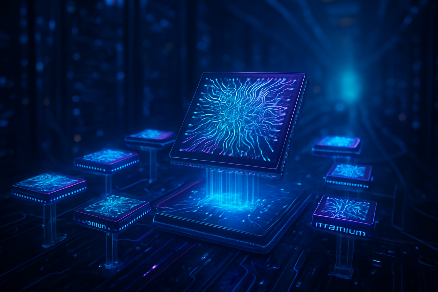
    The semiconductor industry has reached a historic inflection point in late 2025, marking the definitive end of the "Big Iron" era of monolithic chip design. For decades, the goal of silicon engineering was to cram as many transistors as possible onto a single, continuous slab of silicon. However, as artificial intelligence models have scaled into the tens of trillions of parameters, the physical and economic limits of this "monolithic" approach have finally shattered. In its place, a modular revolution has taken hold: the shift to chiplet architectures.

    This transition represents a fundamental reimagining of how computers are built. Rather than a single massive processor, modern AI accelerators like the NVIDIA (NASDAQ: NVDA) Rubin and AMD (NASDAQ: AMD) Instinct MI400 are now constructed like high-tech LEGO sets. By breaking a processor into smaller, specialized "chiplets"—some for intense mathematical calculation, others for memory management or high-speed data transfer—manufacturers are overcoming the "reticle limit," the physical boundary of how large a single chip can be printed. This modularity is not just a technical curiosity; it is the primary engine allowing AI performance to continue doubling even as traditional Moore’s Law scaling slows to a crawl.

    Breaking the Reticle Limit: The Physics of Modular Silicon

    The technical catalyst for the chiplet shift is the "reticle limit," a physical constraint of lithography machines that prevents them from printing a single chip larger than approximately 858mm². As of late 2025, the demand for AI compute has far outstripped what can fit within that tiny square. To solve this, manufacturers are using advanced packaging techniques like TSMC (NYSE: TSM) CoWoS-L (Chip-on-Wafer-on-Substrate with Local Silicon Interconnect) to "stitch" multiple dies together. The recently unveiled NVIDIA Rubin architecture, for instance, effectively creates a "4x reticle" footprint, enabling a level of compute density that would be physically impossible to manufacture as a single piece of silicon.

    Beyond sheer size, the move to chiplets has solved the industry’s most pressing economic headache: yield rates. In a monolithic 3nm design, a single microscopic defect can ruin an entire $10,000 chip. By disaggregating the design into smaller chiplets, manufacturers can test each module individually as a "Known Good Die" (KGD) before assembly. This has pushed effective manufacturing yields for top-tier AI accelerators from the 50-60% range seen in 2023 to over 85% today. If one small chiplet is defective, only that tiny piece is discarded, drastically reducing waste and stabilizing the astronomical costs of leading-edge semiconductor fabrication.

    Furthermore, chiplets enable "heterogeneous integration," allowing engineers to mix and match different manufacturing processes within the same package. In a 2025-era AI processor, the core "brain" might be built on an expensive, ultra-efficient 2nm or 3nm node, while the less-sensitive I/O and memory controllers remain on more mature, cost-effective 5nm or 7nm nodes. This "node optimization" ensures that every dollar of capital expenditure is directed toward the components that provide the greatest performance benefit, preventing a total collapse of the price-to-performance ratio in the AI sector.

    Initial reactions from the AI research community have been overwhelmingly positive, particularly regarding the integration of HBM4 (High Bandwidth Memory). By stacking memory chiplets directly on top of or adjacent to the compute dies, manufacturers are finally bridging the "memory wall"—the bottleneck where processors sit idle while waiting for data. Experts at the 2025 IEEE International Solid-State Circuits Conference noted that this modular approach has enabled a 400% increase in memory bandwidth over the last two years, a feat that would have been unthinkable under the old monolithic paradigm.

    Strategic Realignment: Hyperscalers and the Custom Silicon Moat

    The chiplet revolution has fundamentally altered the competitive landscape for tech giants and AI labs. No longer content to be mere customers of the major chipmakers, hyperscalers like Amazon (NASDAQ: AMZN), Alphabet (NASDAQ: GOOGL), and Meta (NASDAQ: META) have become architects of their own modular silicon. Amazon’s recently launched Trainium3, for example, utilizes a dual-chiplet design that allows AWS to offer AI training credits at nearly 60% lower costs than traditional GPU instances. By using chiplets to lower the barrier to entry for custom hardware, these companies are building a "silicon moat" that optimizes their specific internal workloads, such as recommendation engines or large language model (LLM) inference.

    For established chipmakers, the transition has sparked a fierce strategic battle over packaging dominance. While NVIDIA (NASDAQ: NVDA) remains the performance king with its Rubin and Blackwell platforms, Intel (NASDAQ: INTC) has leveraged its Foveros 3D packaging technology to secure massive foundry wins, including Microsoft (NASDAQ: MSFT) and its Maia 200 series. Intel’s ability to offer "Secure Enclave" manufacturing within the United States has become a significant strategic advantage as geopolitical tensions continue to cloud the future of the global supply chain. Meanwhile, Samsung (KRX: 005930) has positioned itself as a "one-stop shop," integrating its own HBM4 memory with proprietary 2.5D packaging to offer a vertically integrated alternative to the TSMC-NVIDIA duopoly.

    The disruption extends to the startup ecosystem as well. The maturation of the UCIe 3.0 (Universal Chiplet Interconnect Express) standard has created a "Chiplet Economy," where smaller hardware startups like Tenstorrent and Etched can buy "off-the-shelf" I/O and memory chiplets. This allows them to focus their limited R&D budgets on designing a single, high-value AI logic chiplet rather than an entire complex SoC. This democratization of hardware design has reduced the capital required for a first-generation tape-out by an estimated 40%, leading to a surge in specialized AI hardware tailored for niche applications like edge robotics and medical diagnostics.

    The Wider Significance: A New Era for Moore’s Law

    The shift to chiplets is more than a manufacturing tweak; it is the birth of "Moore’s Law 2.0." While the physical shrinking of transistors is reaching its atomic limit, the ability to scale systems through modularity provides a new path forward for the AI landscape. This trend fits into the broader move toward "system-level" scaling, where the unit of compute is no longer a single chip or even a single server, but the entire data center rack. As we move through the end of 2025, the industry is increasingly viewing the data center as one giant, disaggregated computer, with chiplets serving as the interchangeable components of its massive brain.

    However, this transition is not without concerns. The complexity of testing and assembling multi-die packages is immense, and the industry’s heavy reliance on TSMC (NYSE: TSM) for advanced packaging remains a significant single point of failure. Furthermore, as chips become more modular, the power density within a single package has skyrocketed, leading to unprecedented thermal management challenges. The shift toward liquid cooling and even co-packaged optics is no longer a luxury but a requirement for the next generation of AI infrastructure.

    Comparatively, the chiplet milestone is being viewed by industry historians as significant as the transition from vacuum tubes to transistors, or the move from single-core to multi-core CPUs. It represents a shift from a "fixed" hardware mindset to a "fluid" one, where hardware can be as iterative and modular as the software it runs. This flexibility is crucial in a world where AI models are evolving faster than the 18-to-24-month design cycle of traditional semiconductors.

    The Horizon: Glass Substrates and Optical Interconnects
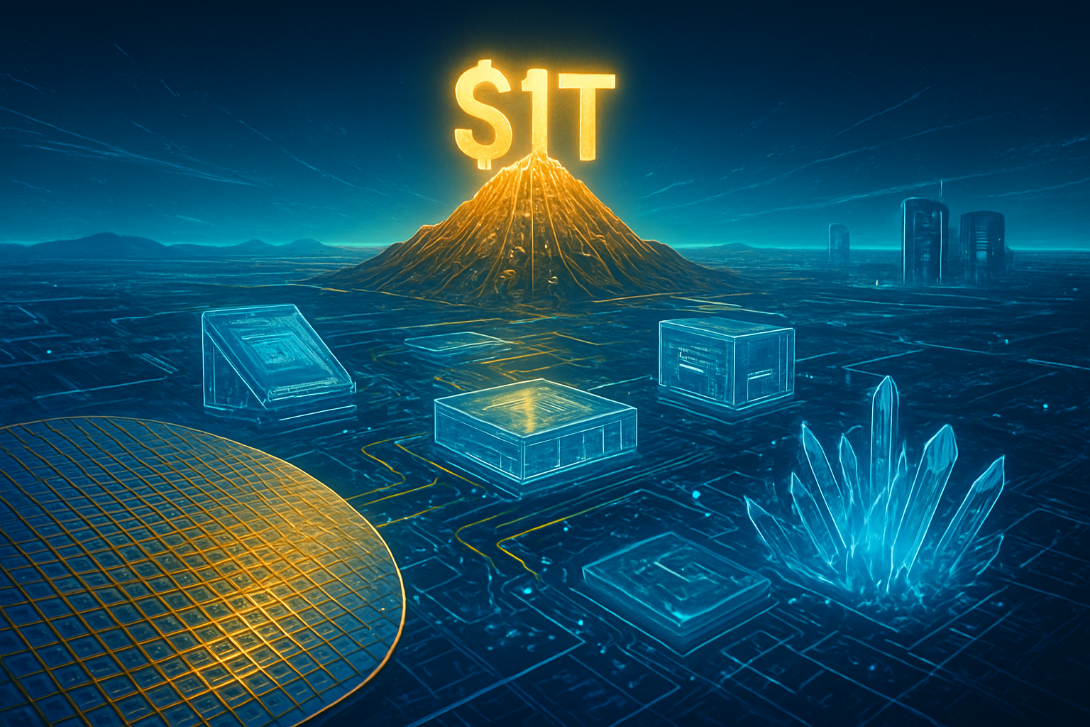
    Looking toward 2026 and beyond, the industry is already preparing for the next phase of the chiplet evolution. One of the most anticipated near-term developments is the commercialization of glass core substrates. Led by research from Intel (NASDAQ: INTC) and TSMC (NYSE: TSM), glass offers superior flatness and thermal stability compared to the organic materials used today. This will allow for even larger package sizes, potentially accommodating up to 12 or 16 HBM4 stacks on a single interposer, further pushing the boundaries of memory capacity for the next generation of "Super-LLMs."

    Another frontier is the integration of Co-Packaged Optics (CPO). As data moves between chiplets, traditional electrical signals generate significant heat and consume a large portion of the chip’s power budget. Experts predict that by late 2026, we will see the first widespread use of optical chiplets that use light rather than electricity to move data between dies. This would effectively eliminate the "communication wall," allowing for near-instantaneous data transfer across a rack of thousands of chips, turning a massive cluster into a single, unified compute engine.

    The challenges ahead are primarily centered on standardization and software. While UCIe has made great strides, ensuring that a chiplet from one vendor can talk seamlessly to a chiplet from another remains a hurdle. Additionally, compilers and software stacks must become "chiplet-aware" to efficiently distribute workloads across these fragmented architectures. Nevertheless, the trajectory is clear: the future of AI is modular.

    Conclusion: The Modular Future of Intelligence

    The shift from monolithic to chiplet architectures marks the most significant architectural change in the semiconductor industry in decades. By overcoming the physical limits of lithography and the economic barriers of declining yields, chiplets have provided the runway necessary for the AI revolution to continue its exponential growth. The success of platforms like NVIDIA’s Rubin and AMD’s MI400 has proven that the "LEGO-like" approach to silicon is not just viable, but essential for the next decade of compute.

    As we look toward 2026, the key takeaways are clear: packaging is the new Moore’s Law, custom silicon is the new strategic moat for hyperscalers, and the "deconstruction" of the data center is well underway. The industry has moved from asking "how small can we make a chip?" to "how many pieces can we connect?" This change in perspective ensures that while the physical limits of silicon may be in sight, the limits of artificial intelligence remain as distant as ever. In the coming months, watch for the first high-volume deployments of HBM4 and the initial pilot programs for glass substrates—these will be the bellwethers for the next stage of the modular era.


    This content is intended for informational purposes only and represents analysis of current AI developments.

    TokenRing AI delivers enterprise-grade solutions for multi-agent AI workflow orchestration, AI-powered development tools, and seamless remote collaboration platforms.
    For more information, visit https://www.tokenring.ai/.

  • The Memory Wall: Why HBM4 is the New Frontier in the Global AI Arms Race

    The Memory Wall: Why HBM4 is the New Frontier in the Global AI Arms Race

    As of late 2025, the artificial intelligence revolution has reached a critical inflection point where the speed of silicon is no longer the primary constraint. Instead, the industry’s gaze has shifted to the "Memory Wall"—the physical limit of how fast data can move between a processor and its memory. High Bandwidth Memory (HBM) has emerged as the most precious commodity in the tech world, serving as the essential fuel for the massive Large Language Models (LLMs) and generative AI systems that now define the global economy.

    The announcement of Nvidia’s (NASDAQ: NVDA) upcoming "Rubin" architecture, which utilizes the next-generation HBM4 standard, has sent shockwaves through the semiconductor industry. With HBM supply already sold out through most of 2026, the competition between the world’s three primary producers—SK Hynix, Micron, and Samsung—has escalated into a high-stakes battle for dominance in a market that is fundamentally reshaping the hardware landscape.

    The Technical Leap: From HBM3e to the 2048-bit HBM4 Era

    The technical specifications of HBM in late 2025 reveal a staggering jump in capability. While HBM3e was the workhorse of the Blackwell GPU generation, offering roughly 1.2 TB/s of bandwidth per stack, the new HBM4 standard represents a paradigm shift. The most significant advancement is the doubling of the memory interface width from 1024-bit to 2048-bit. This allows HBM4 to achieve bandwidths exceeding 2.0 TB/s per stack while maintaining lower clock speeds, a crucial factor in managing the extreme heat generated by 12-layer and 16-layer 3D-stacked dies.

    This generational shift is not just about speed; it is about capacity and physical integration. As of December 2025, the industry has transitioned to "1c" DRAM nodes (approximately 10nm), enabling capacities of up to 64GB per stack. Furthermore, the integration process has evolved. Using TSMC’s (NYSE: TSM) System on Integrated Chips (SoIC) and "bumpless" hybrid bonding, HBM4 stacks are now placed within microns of the GPU logic die. This proximity drastically reduces electrical impedance and power consumption, which had become a major barrier to scaling AI clusters.

    Industry experts note that this transition is technically grueling. The shift to HBM4 requires a total redesign of the base logic die—the foundation upon which memory layers are stacked. Unlike previous generations where the logic die was relatively simple, HBM4 logic dies are increasingly being manufactured on advanced 5nm or 3nm foundry processes to handle the complex routing required for the 2048-bit interface. This has turned HBM from a "commodity" component into a semi-custom processor in its own right.

    The Titan Triumvirate: SK Hynix, Micron, and Samsung’s Power Struggle

    The competitive landscape of late 2025 is dominated by an intense three-way rivalry. SK Hynix (KRX: 000660) currently holds the throne with an estimated 55–60% market share. Their early bet on Mass Reflow Molded Underfill (MR-MUF) packaging technology has paid off, providing superior thermal dissipation that has made them the preferred partner for Nvidia’s Blackwell Ultra (B300) systems. In December 2025, SK Hynix became the first to ship verified HBM4 samples for the Rubin platform, solidifying its lead.

    Micron (NASDAQ: MU) has successfully cemented itself as the primary challenger, holding approximately 20–25% of the market. Micron’s 12-layer HBM3e stacks gained widespread acclaim in early 2025 for their industry-leading power efficiency, which allowed data center operators to squeeze more performance out of existing power envelopes. However, as the industry moves toward HBM4, Micron faces the challenge of scaling its "1c" node yields to match the aggressive production schedules of major cloud providers like Microsoft (NASDAQ: MSFT) and Google (NASDAQ: GOOGL).

    Samsung (KRX: 005930), after a period of qualification delays in 2024, has mounted a massive comeback in late 2025. Samsung is playing a unique strategic card: the "One-Stop Shop." As the only company that possesses both world-class DRAM manufacturing and a leading-edge logic foundry, Samsung is offering "Custom HBM" solutions. By manufacturing both the memory layers and the specialized logic die in-house, Samsung aims to bypass the complex supply chain coordination required between memory makers and external foundries like TSMC, a move that is gaining traction with hyperscalers looking for bespoke AI silicon.

    The Critical Link: Why LLMs Live and Die by Memory Bandwidth

    The criticality of HBM for generative AI cannot be overstated. In late 2025, the AI industry has bifurcated its needs into two distinct categories: training and inference. For training trillion-parameter models, bandwidth is the absolute priority. Without the 13.5 TB/s aggregate bandwidth provided by HBM4-equipped GPUs, the thousands of processing cores inside an AI chip would spend a significant portion of their cycles "starving" for data, leading to massive inefficiencies in multi-billion dollar training runs.

    For inference, the focus has shifted toward capacity. The rise of "Agentic AI" and long-context windows—where models can remember and process up to 2 million tokens of information—requires massive amounts of VRAM to store the "KV Cache" (the model's short-term memory). A single GPU now needs upwards of 288GB of HBM to handle high-concurrency requests for complex agents. This demand has led to a persistent supply shortage, with lead times for HBM-equipped hardware exceeding 40 weeks for smaller firms.

    Furthermore, the HBM boom is having a "cannibalization" effect on the broader tech industry. Because HBM requires roughly three times the wafer area of standard DDR5 memory, the surge in AI demand has restricted the supply of PC and server RAM. As of December 2025, commodity DRAM prices have surged by over 60% year-over-year, impacting everything from consumer laptops to enterprise cloud storage. This "AI tax" is now a standard consideration for IT departments worldwide.

    Future Horizons: Custom Logic and the Road to HBM5

    Looking ahead to 2026 and beyond, the roadmap for HBM is moving toward even deeper integration. The next phase, often referred to as HBM4e, is expected to push capacities toward 80GB per stack. However, the more profound change will be the "logic-on-memory" trend. Experts predict that future HBM stacks will incorporate specialized AI accelerators directly into the base logic die, allowing for "near-memory computing" where simple data processing tasks are handled within the memory stack itself, further reducing the need to move data back and forth to the main GPU.

    Challenges remain, particularly regarding yield and cost. Producing HBM4 at the "1c" node is proving to be one of the most difficult manufacturing feats in semiconductor history. Current yields for 16-layer stacks are reportedly hovering around 60%, meaning nearly half of the highly expensive wafers are discarded. Addressing these yield issues will be the primary focus for engineers in the coming months, as any improvement directly translates to millions of dollars in additional revenue for the manufacturers.

    The Final Verdict on the HBM Revolution

    High Bandwidth Memory has transitioned from a niche hardware specification to the geopolitical and economic linchpin of the AI era. As we close out 2025, it is clear that the companies that control the memory supply—SK Hynix, Micron, and Samsung—hold as much power over the future of AI as the companies designing the chips or the models themselves. The shift to HBM4 marks a new chapter where memory is no longer just a storage medium, but a sophisticated, high-performance compute platform.

    In the coming months, the industry should watch for the first production benchmarks of Nvidia’s Rubin GPUs and the success of Samsung’s integrated foundry-memory model. As AI models continue to grow in complexity and context, the "Memory Wall" will either be the barrier that slows progress or, through the continued evolution of HBM, the foundation upon which the next generation of digital intelligence is built.


    This content is intended for informational purposes only and represents analysis of current AI developments.

    TokenRing AI delivers enterprise-grade solutions for multi-agent AI workflow orchestration, AI-powered development tools, and seamless remote collaboration platforms.
    For more information, visit https://www.tokenring.ai/.

  • The Rise of Sovereign AI: Why Nations are Racing to Build Their Own Silicon Ecosystems

    The Rise of Sovereign AI: Why Nations are Racing to Build Their Own Silicon Ecosystems

    As of late 2025, the global technology landscape has shifted from a race for software dominance to a high-stakes battle for "Sovereign AI." No longer content with renting compute power from a handful of Silicon Valley giants, nations are aggressively building their own end-to-end AI stacks—encompassing domestic data, indigenous models, and, most critically, homegrown semiconductor ecosystems. This movement represents a fundamental pivot in geopolitics, where digital autonomy is now viewed as the ultimate prerequisite for national security and economic survival.

    The urgency behind this trend is driven by a desire to escape the "compute monopoly" held by a few major players. By investing billions into custom silicon and domestic fabrication, countries like Japan, India, France, and the UAE are attempting to insulate themselves from supply chain shocks and foreign export controls. The result is a fragmented but rapidly innovating global market where "AI nationalism" is the new status quo, fueling an unprecedented demand for specialized hardware tailored to local languages, cultural norms, and specific industrial needs.

    The Technical Frontier: From General GPUs to Custom ASICs

    The technical backbone of the Sovereign AI movement is a shift away from general-purpose hardware toward Application-Specific Integrated Circuits (ASICs) and advanced fabrication nodes. In Japan, the government-backed venture Rapidus, in collaboration with IBM (NYSE: IBM), has accelerated its timeline to achieve mass production of 2nm logic chips by 2027. This leap is designed to power a new generation of domestic AI supercomputers that prioritize energy efficiency—a critical factor as AI power consumption threatens national grids. Japan’s Sakura Internet (TYO: 3778) has already deployed massive clusters utilizing NVIDIA (NASDAQ: NVDA) Blackwell architecture, but the long-term goal remains a transition to Japanese-designed silicon.

    In India, the technical focus has landed on the "IndiaAI Mission," which recently saw the deployment of the PARAM Rudra supercomputer series across major academic hubs. Unlike previous iterations, these systems are being integrated with India’s first indigenously designed 3nm chips, aimed at processing "Vikas" (developmental) data. Meanwhile, in France, the Jean Zay supercomputer is being augmented with wafer-scale engines from companies like Cerebras, allowing for the training of massive foundation models like those from Mistral AI without the latency overhead of traditional GPU clusters.

    This shift differs from previous approaches because it prioritizes "data residency" at the hardware level. Sovereign systems are being designed with hardware-level encryption and "clean room" environments that ensure sensitive state data never leaves domestic soil. Industry experts note that this is a departure from the "cloud-first" era, where data was often processed in whichever jurisdiction offered the cheapest compute. Now, the priority is "trusted silicon"—hardware whose entire provenance, from design to fabrication, can be verified by the state.

    Market Disruptions and the Rise of the "National Stack"

    The push for Sovereign AI is creating a complex web of winners and losers in the corporate world. While NVIDIA (NASDAQ: NVDA) remains the dominant provider of AI training hardware, the rise of national initiatives is forcing the company to adapt its business model. NVIDIA has increasingly moved toward "Sovereign AI as a Service," helping nations build local data centers while navigating complex export regulations. However, the move toward custom silicon presents a long-term threat to NVIDIA’s dominance, as nations look to AMD (NASDAQ: AMD), Broadcom (NASDAQ: AVGO), and Marvell Technology (NASDAQ: MRVL) for custom ASIC design services.

    Cloud giants like Oracle (NYSE: ORCL) and Microsoft (NASDAQ: MSFT) are also pivoting. Oracle has been particularly aggressive in the Middle East, partnering with the UAE’s G42 to build the "Stargate UAE" cluster—a 1-gigawatt facility that functions as a sovereign cloud. This strategic positioning allows these tech giants to remain relevant by acting as the infrastructure partners for national projects, even as those nations move toward hardware independence. Conversely, startups specializing in AI inferencing, such as Groq, are seeing massive inflows of sovereign wealth, with Saudi Arabia’s Alat investing heavily to build the world’s largest inferencing hub in the Kingdom.

    The competitive landscape is also seeing the emergence of "Regional Champions." Companies like Samsung Electronics (KRX: 005930) and TSMC (NYSE: TSM) are being courted by nations with hundred-billion-dollar incentives to build domestic mega-fabs. The UAE, for instance, is currently in advanced negotiations to bring TSMC production to the Gulf, a move that would fundamentally alter the semiconductor supply chain and reduce the world's reliance on the Taiwan Strait.

    Geopolitical Significance and the New "Oil"

    The broader significance of Sovereign AI cannot be overstated; it is the "space race" of the 21st century. In 2025, data is no longer just "the new oil"—it is the refined fuel that powers national intelligence. By building domestic AI ecosystems, nations are ensuring that the economic "rent" generated by AI stays within their borders. France’s President Macron recently highlighted this, noting that a nation that exports its raw data to buy back "foreign intelligence" is effectively a digital colony.

    However, this trend brings significant concerns regarding fragmentation. As nations build AI models aligned with their own cultural and legal frameworks, the "splinternet" is evolving into the "split-intelligence" era. A model trained on Saudi values may behave fundamentally differently from one trained on French or Indian data. This raises questions about global safety standards and the ability to regulate AI on an international scale. If every nation has its own "sovereign" black box, finding common ground on AI alignment and existential risk becomes exponentially more difficult.

    Comparatively, this milestone mirrors the development of national nuclear programs in the mid-20th century. Just as nuclear energy and weaponry became the hallmarks of a superpower, AI compute capacity is now the metric of a nation's "hard power." The "Pax Silica" alliance—a group including the U.S., Japan, and South Korea—is an attempt to create a "trusted" supply chain, effectively creating a technological bloc that stands in opposition to the AI development tracks of China and its partners.

    The Horizon: 2nm Production and Beyond

    Looking ahead, the next 24 to 36 months will be defined by the "Tapeout Race." Saudi Arabia is expected to see its first domestically designed AI chips hit the market by mid-2026, while Japan’s Rapidus aims to have its 2nm pilot line operational by late 2025. These developments will likely lead to a surge in edge-AI applications, where custom silicon allows for high-performance AI to be embedded in everything from national power grids to autonomous defense systems without needing a constant connection to a centralized cloud.

    The long-term challenge remains the talent war. While a nation can buy GPUs and build fabs, the specialized engineering talent required to design world-class silicon is still concentrated in a few global hubs. Experts predict that we will see a massive increase in "educational sovereignism," with countries like India and the UAE launching aggressive programs to train hundreds of thousands of semiconductor engineers. The ultimate goal is a "closed-loop" ecosystem where a nation can design, manufacture, and train AI entirely within its own borders.

    A New Era of Digital Autonomy

    The rise of Sovereign AI marks the end of the era of globalized, borderless technology. As of December 2025, the "National Stack" has become the standard for any country with the capital and ambition to compete on the world stage. The race to build domestic semiconductor ecosystems is not just about chips; it is about the preservation of national identity and the securing of economic futures in an age where intelligence is the primary currency.

    In the coming months, watchers should keep a close eye on the "Stargate" projects in the Middle East and the progress of the Rapidus 2nm facility in Japan. These projects will serve as the litmus test for whether a nation can truly break free from the gravity of Silicon Valley. While the challenges are immense—ranging from energy constraints to talent shortages—the momentum behind Sovereign AI is now irreversible. The map of the world is being redrawn, one transistor at a time.


    This content is intended for informational purposes only and represents analysis of current AI developments.

    TokenRing AI delivers enterprise-grade solutions for multi-agent AI workflow orchestration, AI-powered development tools, and seamless remote collaboration platforms.
    For more information, visit https://www.tokenring.ai/.

  • Broadcom’s 20% AI Correction: Why the ‘Plumbing of the Internet’ Just Hit a Major Speed Bump

    Broadcom’s 20% AI Correction: Why the ‘Plumbing of the Internet’ Just Hit a Major Speed Bump

    As of December 18, 2025, the semiconductor landscape is grappling with a paradox: Broadcom Inc. (NASDAQ: AVGO) is reporting record-breaking demand for its artificial intelligence infrastructure, yet its stock has plummeted more than 20% from its December 9 all-time high of $414.61. This sharp correction, which has seen shares retreat to the $330 range in just over a week, has sent shockwaves through the tech sector. While the company’s Q4 fiscal 2025 earnings beat expectations, a confluence of "margin anxiety," a "sell the news" reaction to a massive OpenAI partnership, and broader valuation concerns have triggered a significant reset for the networking giant.

    The immediate significance of this dip lies in the growing tension between Broadcom’s market-share dominance and its shifting profitability profile. As the primary provider of custom AI accelerators (XPUs) and high-end Ethernet switching for hyperscalers like Google (NASDAQ: GOOGL) and Meta Platforms, Inc. (NASDAQ: META), Broadcom is the undisputed "plumbing" of the AI revolution. However, the transition from selling high-margin individual chips to complex, integrated system-level solutions has introduced a new variable: margin compression. Investors are now forced to decide if the current 21% discount represents a generational entry point or the first crack in the "AI infrastructure supercycle."

    The Technical Engine: Tomahawk 6 and the Custom Silicon Pivot

    The technical catalyst behind Broadcom's current market position—and its recent volatility—is the aggressive rollout of its next-generation networking stack. In late 2025, Broadcom began volume shipping the Tomahawk 6 (TH6-Davisson), the world’s first 102.4 Tbps Ethernet switch. This chip doubles the bandwidth of its predecessor and, for the first time, widely implements Co-Packaged Optics (CPO). By integrating optical components directly onto the silicon package, Broadcom has managed to slash power consumption in 100,000+ GPU clusters—a critical requirement as data centers hit the "power wall."

    Beyond networking, Broadcom’s custom ASIC (Application-Specific Integrated Circuit) business has become its primary growth engine. The company now holds an estimated 89% market share in this space, co-developing "XPUs" that are optimized for specific AI workloads. Unlike general-purpose GPUs from NVIDIA Corporation (NASDAQ: NVDA), these custom chips are architected for maximum efficiency in inference—the process of running AI models. The recent technical milestone of the Ultra Ethernet Consortium (UEC) 1.0 specification has further empowered Broadcom, allowing its Ethernet fabric to achieve sub-2ms latency, effectively neutralizing the performance advantage previously held by Nvidia’s proprietary InfiniBand interconnect.

    However, these technical triumphs come with a financial caveat. To win the "inference war," Broadcom has moved toward delivering full-rack solutions that include lower-margin third-party components like High Bandwidth Memory (HBM4). This shift led to management's guidance of a 100-basis-point gross margin compression for early 2026. While the technical community views the move to integrated systems as a brilliant strategic "lock-in" play, the financial community reacted with "margin jitters," viewing the dip in percentage points as a potential sign of waning pricing power.

    The Hyperscale Impact: OpenAI, Meta, and the 'Nvidia Tax'

    The ripple effects of Broadcom’s stock dip are being felt across the "Magnificent Seven" and the broader AI lab ecosystem. The most significant development of late 2025 was the confirmation of a landmark 10-gigawatt (GW) deal with OpenAI. This multi-year partnership aims to co-develop custom accelerators and networking for OpenAI’s future AGI-class models. While the deal is projected to yield up to $150 billion in revenue through 2029, the market’s "sell the news" reaction suggests that investors are weary of the long lead times—meaningful revenue from the OpenAI deal isn't expected to hit the balance sheet until 2027.

    For competitors like Marvell Technology, Inc. (NASDAQ: MRVL), Broadcom’s dip is a double-edged sword. While Marvell is growing faster from a smaller base, Broadcom’s scale remains a massive barrier to entry. Broadcom’s current AI backlog stands at a staggering $73 billion, nearly ten times Marvell's total annual revenue. This backlog provides a safety net for Broadcom, even as its stock price wavers. By providing a credible, open-standard alternative to Nvidia’s vertically integrated "walled garden," Broadcom has become the preferred partner for tech giants looking to avoid the "Nvidia tax"—the high premium and supply constraints associated with the H200 and Blackwell series.

    The strategic advantage for companies like Google and Meta is clear: by using Broadcom’s custom silicon, they can optimize hardware for their specific software stacks (like Google’s TPU v7), resulting in a lower "cost per token." This efficiency is becoming the primary metric for success as the industry shifts from training massive models to serving them to billions of users at scale.

    Wider Significance: The Great Networking War and the AI Landscape

    Broadcom’s 20% correction marks a pivotal moment in the broader AI landscape, signaling a shift from speculative hype to "execution reality." For the past two years, the market has rewarded any company associated with AI infrastructure with sky-high valuations. Broadcom’s peak 42x forward earnings multiple was a testament to this optimism. However, the mid-December 2025 correction suggests that the market is beginning to differentiate between "growth at any cost" and "sustainable margin growth."

    A major trend highlighted by this event is the definitive victory of Ethernet over InfiniBand for large-scale AI inference. As clusters grow toward the "one million XPU" mark, the economics of proprietary networking like Nvidia’s InfiniBand become untenable. Broadcom’s push for open standards via the Ultra Ethernet Consortium has successfully commoditized high-performance networking, making it accessible to a wider range of players. This democratization of high-speed interconnects is essential for the next phase of AI development, where smaller labs and startups will need to compete with the compute-rich giants.

    Furthermore, Broadcom’s situation mirrors previous tech milestones, such as the transition from mainframe to client-server or the early days of cloud infrastructure. In each case, the "plumbing" providers initially saw margin compression as they scaled, only to emerge as high-margin monopolies once the infrastructure became indispensable. Industry experts from firms like JP Morgan and Goldman Sachs argue that the current dip is a "tactical buying opportunity," as the absolute dollar growth in Broadcom’s AI business far outweighs the percentage-point dip in gross margins.

    Future Horizons: 1-Million-XPU Clusters and the Road to 2027

    Looking ahead, Broadcom’s roadmap focuses on the "scale-out" architecture required for Artificial General Intelligence (AGI). Expected developments in 2026 include the launch of the Jericho 4 routing series, designed to handle the massive data flows of clusters exceeding one million accelerators. These clusters will likely be powered by the 3nm and 2nm processes from Taiwan Semiconductor Manufacturing Company (NYSE: TSM), with whom Broadcom maintains a deep strategic partnership.

    The most anticipated milestone is the H2 2026 deployment of the OpenAI custom chips. If these accelerators perform as expected, they could fundamentally change the economics of AI, potentially reducing the cost of running advanced models by as much as 40%. However, challenges remain. The integration of Co-Packaged Optics (CPO) is technically difficult and requires a complete overhaul of data center cooling and maintenance protocols. Furthermore, the geopolitical landscape remains a wildcard, as any further restrictions on high-end silicon exports could disrupt Broadcom's global supply chain.

    Experts predict that Broadcom will continue to trade with high volatility throughout 2026 as the market digests the massive $73 billion backlog. The key metric to watch will not be the stock price, but the "cost per token" achieved by Broadcom’s custom silicon partners. If Broadcom can prove that its system-level approach leads to superior ROI for hyperscalers, the current 20% dip will likely be remembered as a minor blip in a decade-long expansion.

    Summary and Final Thoughts

    Broadcom’s recent 20% stock correction is a complex event that blends technical evolution with financial recalibration. While "margin anxiety" and valuation concerns have cooled investor enthusiasm in the short term, the company’s underlying fundamentals—driven by the Tomahawk 6, the OpenAI partnership, and a dominant position in the custom ASIC market—remain robust. Broadcom has successfully positioned itself as the open-standard alternative to the Nvidia ecosystem, a strategic move that is now yielding a $73 billion backlog.

    In the history of AI, this period may be seen as the "Inference Inflection Point," where the focus shifted from building the biggest models to building the most efficient ones. Broadcom’s willingness to sacrifice short-term margin percentages for long-term system-level lock-in is a classic Hock Tan strategy that has historically rewarded patient investors.

    As we move into 2026, the industry will be watching for the first results of the Tomahawk 6 deployments and any updates on the OpenAI silicon timeline. For now, the "plumbing of the internet" is undergoing a major upgrade, and while the installation is proving expensive, the finished infrastructure promises to power the next generation of human intelligence.


    This content is intended for informational purposes only and represents analysis of current AI developments.

    TokenRing AI delivers enterprise-grade solutions for multi-agent AI workflow orchestration, AI-powered development tools, and seamless remote collaboration platforms.
    For more information, visit https://www.tokenring.ai/.