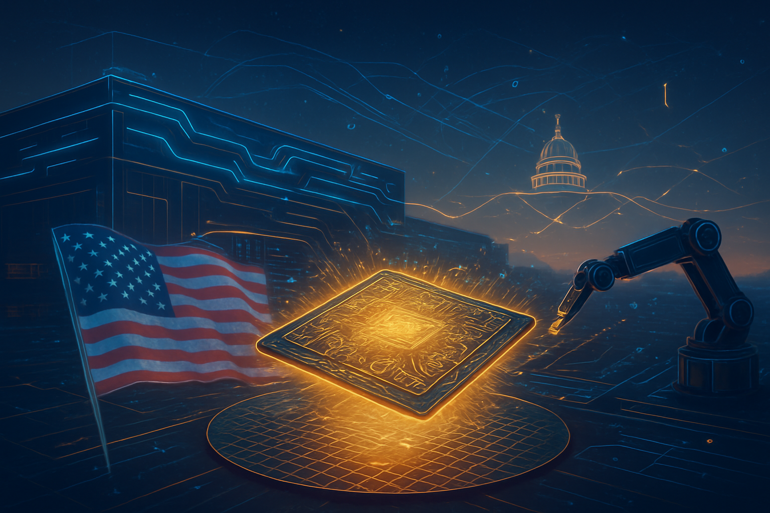
As of December 23, 2025, the landscape of global semiconductor manufacturing has reached a pivotal turning point. Taiwan Semiconductor Manufacturing Company (NYSE: TSM), the world’s leading contract chipmaker, has officially accelerated its roadmap for its sprawling Fab 21 complex in Phoenix, Arizona. With Phase 1 already churning out high volumes of 4nm and 5nm silicon, the company has confirmed that early equipment installation and cleanroom preparation for Phase 2—the facility’s 3nm production line—are well underway. This development marks a significant victory for the U.S. strategy to repatriate critical technology infrastructure and secure the supply chain for the next generation of artificial intelligence.
The acceleration of the Arizona site, which was once plagued by labor disputes and construction delays, signals a newfound confidence in the American "Silicon Desert." By pulling forward the timeline for 3nm production to 2027—a full year ahead of previous estimates—TSMC is responding to insatiable demand from domestic tech giants who are eager to insulate their AI hardware from geopolitical volatility in the Pacific.
Technical Milestones and the 92% Yield Breakthrough
The technical prowess displayed at Fab 21 has silenced many early skeptics of U.S.-based advanced manufacturing. In a milestone report released late this year, TSMC (NYSE: TSM) revealed that its Arizona Phase 1 facility has achieved a 4nm yield rate of 92%. Remarkably, this figure is approximately four percentage points higher than the yields achieved at equivalent facilities in Taiwan. This success is attributed to the implementation of "Digital Twin" manufacturing technology, where a virtual model of the fab allows engineers to simulate and optimize processes in real-time before they are executed on the physical floor.
The transition to 3nm (N3) technology in Phase 2 represents a massive leap in transistor density and energy efficiency. The 3nm process is expected to offer up to a 15% speed improvement at the same power level or a 30% power reduction at the same speed compared to the 5nm node. As of December 2025, the physical shell of the Phase 2 fab is complete, and the installation of internal infrastructure—including hyper-cleanroom HVAC systems and specialized chemical delivery networks—is progressing rapidly. The primary "tool-in" phase, involving the move-in of multi-million dollar Extreme Ultraviolet (EUV) lithography machines, is now slated for early 2026, setting the stage for volume production in 2027.
A Windfall for AI Giants and the End-to-End Supply Chain
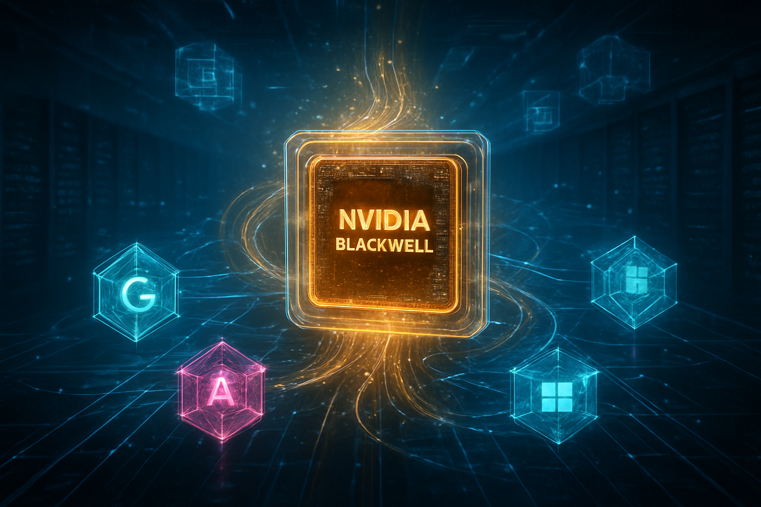
The acceleration of 3nm capabilities in Arizona is a strategic boon for the primary architects of the AI revolution. Apple (NASDAQ: AAPL), NVIDIA (NASDAQ: NVDA), and AMD (NASDAQ: AMD) have already secured the lion's share of the capacity at Fab 21. For NVIDIA, the ability to produce its high-end Blackwell AI processors on U.S. soil reduces the logistical and political risks associated with shipping wafers across the Taiwan Strait. While the front-end wafers are currently the focus, the recent groundbreaking of a $7 billion advanced packaging facility by Amkor Technology (NASDAQ: AMKR) in nearby Peoria, Arizona, is the final piece of the puzzle.
By 2027, the partnership between TSMC and Amkor will enable a "100% American-made" lifecycle for AI chips. Historically, even chips fabricated in the U.S. had to be sent to Taiwan for Chip-on-Wafer-on-Substrate (CoWoS) packaging. The emergence of a domestic packaging ecosystem ensures that companies like NVIDIA and AMD can maintain a resilient, end-to-end supply chain within North America. This shift not only provides a competitive advantage in terms of lead times but also allows these firms to market their products as "sovereign-secure" to government and enterprise clients.
The Geopolitical Significance of the Silicon Desert
The strategic importance of TSMC’s Arizona expansion cannot be overstated. It serves as the crown jewel of the U.S. CHIPS and Science Act, which provided TSMC with $6.6 billion in direct grants and up to $5 billion in loans. As of late 2025, the U.S. Department of Commerce has finalized several tranches of this funding, citing TSMC's ability to meet and exceed its technical milestones. This development places the U.S. in a much stronger position relative to global competitors, including Samsung (KRX: 005930) and Intel (NASDAQ: INTC), both of which are racing to bring their own advanced nodes to market.
This move toward "geographic decoupling" is a direct response to the heightened tensions in the South China Sea. By establishing a "GigaFab" cluster in Arizona—now projected to include a total of six fabs with a total investment of $165 billion—TSMC is creating a high-security alternative to its Taiwan-based operations. This has fundamentally altered the global semiconductor landscape, moving the center of gravity for high-end manufacturing closer to the software and design hubs of Silicon Valley.
Looking Ahead: The Road to 2nm and Beyond
The roadmap for TSMC Arizona does not stop at 3nm. In April 2025, the company broke ground on Phase 3 (Fab 3), which is designated for the even more advanced 2nm (N2) and A16 (1.6nm) angstrom-class process nodes. These technologies will be essential for the next generation of AI models, which will require exponential increases in computational power and efficiency. Experts predict that by 2030, the Arizona complex will be capable of producing the most advanced semiconductors in the world, potentially reaching parity with TSMC’s flagship "Fab 18" in Tainan.
However, challenges remain. The industry continues to grapple with a shortage of specialized talent required to operate these highly automated facilities. While the 92% yield rate suggests that the initial workforce hurdles have been largely overcome, the scale of the expansion—from two fabs to six—will require a massive influx of engineers and technicians over the next five years. Furthermore, the integration of advanced packaging on-site will require a new level of coordination between TSMC and its ecosystem partners.
Conclusion: A New Era for American Silicon
The status of TSMC’s Fab 21 in December 2025 represents a landmark achievement in industrial policy and technological execution. The acceleration of 3nm equipment installation and the surprising yield success of Phase 1 have transformed the "Silicon Desert" from a theoretical ambition into a tangible reality. For the U.S., this facility is more than just a factory; it is a critical safeguard for the future of artificial intelligence and national security.
As we move into 2026, the industry will be watching closely for the arrival of the first EUV tools in Phase 2 and the continued progress of the Phase 3 groundbreaking. With the support of the CHIPS Act and the commitment of the world's largest tech companies, TSMC Arizona has set a new standard for global semiconductor manufacturing, ensuring that the most advanced chips of the future will bear the "Made in USA" label.
This content is intended for informational purposes only and represents analysis of current AI developments.
TokenRing AI delivers enterprise-grade solutions for multi-agent AI workflow orchestration, AI-powered development tools, and seamless remote collaboration platforms.
For more information, visit https://www.tokenring.ai/.