In a definitive move to cement its dominance in the artificial intelligence landscape, NVIDIA (NASDAQ:NVDA) has officially transitioned its next-generation "Vera Rubin" platform into full production. Announced as the successor to the record-breaking Blackwell architecture, the Rubin platform is slated for broad availability in the second half of 2026. This milestone marks a pivotal acceleration in NVIDIA's product roadmap, transitioning the company from a traditional two-year data center release cycle to an aggressive annual cadence designed to keep pace with the exponential demands of generative AI and autonomous agents.
The immediate significance of the Vera Rubin platform lies in its staggering promise: a 10x reduction in inference costs compared to the current Blackwell chips. By drastically lowering the price-per-token for large language models (LLMs) and complex reasoning systems, NVIDIA is not merely launching a faster processor; it is recalibrating the economic feasibility of deploying AI at a global scale. As developers move from simple chatbots to sophisticated "Agentic AI" that can reason and execute multi-step tasks, the Rubin platform arrives as the necessary infrastructure to support the next trillion-dollar shift in the tech economy.
Technical Prowess: The R100 GPU and the HBM4 Revolution
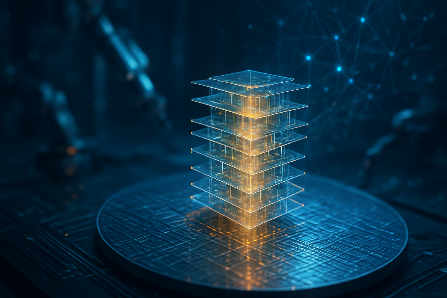
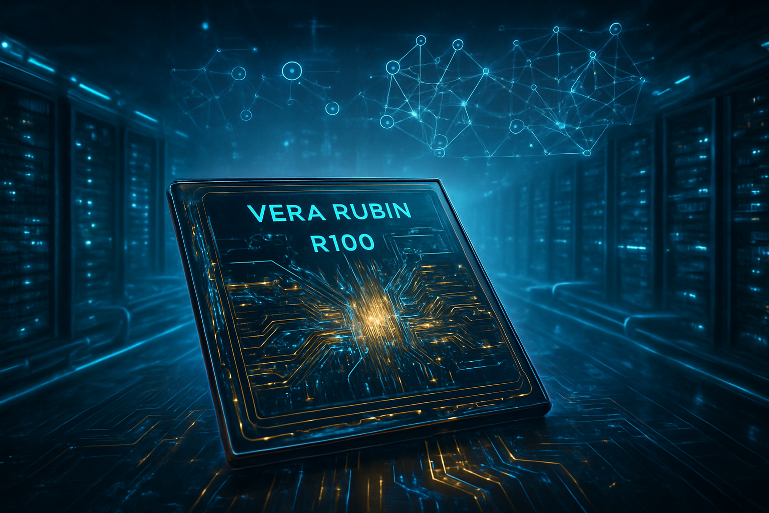
At the heart of the Vera Rubin platform is the R100 GPU, a marvel of semiconductor engineering fabricated on TSMC’s (NYSE:TSM) enhanced N3P (3nm) process. Boasting approximately 336 billion transistors—a massive leap from Blackwell’s 208 billion—the R100 utilizes an advanced chiplet design with 4x reticle size, pushed to the limits by CoWoS-L packaging. This architecture allows NVIDIA to integrate 288GB of High Bandwidth Memory 4 (HBM4), providing an unprecedented 22 TB/s of aggregate bandwidth. This nearly triples the throughput of the Blackwell B200, effectively shattering the "memory wall" that has long throttled AI performance.
The platform further distinguishes itself through the introduction of the Vera CPU, featuring 88 custom "Olympus" ARM-based cores. By pairing the R100 GPU directly with the Vera CPU via NVLink-C2C (1.8 TB/s), NVIDIA has eliminated the traditional latency bottlenecks found in x86-based systems. Furthermore, the new NVLink 6 interconnect offers a 3.6 TB/s bi-directional bandwidth per GPU, enabling the creation of "Million-GPU" clusters. This hardware-software co-design allows the R100 to achieve 50 petaflops of FP4 inference performance, five times the raw compute power of its predecessor.
Initial reactions from the AI research community have been overwhelmingly positive, particularly regarding the third-generation Transformer Engine. Researchers at labs like OpenAI and Anthropic have noted that the R100's hardware-accelerated adaptive compression is specifically tuned for the "reasoning" phase of modern models. Unlike previous chips that focused primarily on raw throughput, Rubin is built for long-context windows and iterative logical processing, which are essential for the next generation of autonomous agents.
Reshaping the Competitive Landscape
The shift to the Rubin platform creates a massive strategic advantage for "Hyperscalers" and elite AI labs. Microsoft (NASDAQ:MSFT), Amazon (NASDAQ:AMZN), and Alphabet (NASDAQ:GOOGL) have already secured significant early allocations for H2 2026. Microsoft, in particular, is reportedly designing its "Fairwater" superfactories specifically around the Rubin NVL72 rack-scale systems. For these tech giants, the 10x reduction in inference costs provides a defensive moat against rising energy costs and the immense capital expenditure required to stay competitive in the AI race.
For startups and smaller AI firms, the Rubin platform represents a double-edged sword. While the reduction in inference costs makes deploying high-end models more affordable, the sheer scale required to utilize Rubin’s full potential may further widen the gap between the "compute rich" and the "compute poor." However, NVIDIA's HGX Rubin NVL8 configuration—designed for standard x86 environments—aims to provide a path for mid-market players to access these efficiencies without rebuilding their entire data center infrastructure from the ground up.
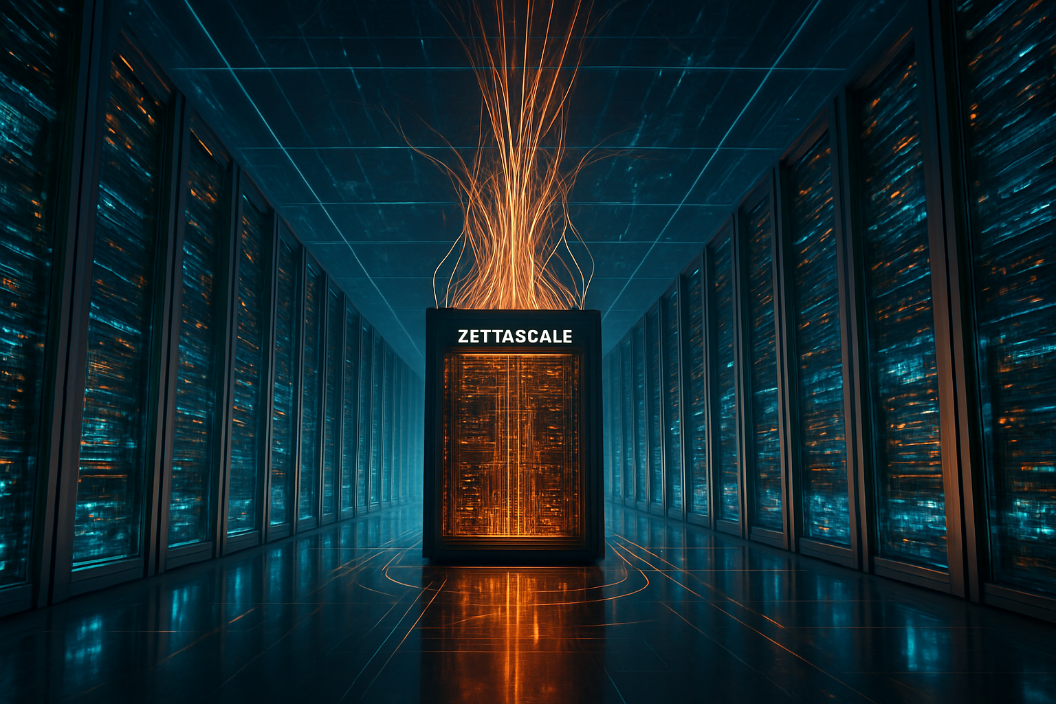
Strategically, Rubin serves as NVIDIA's definitive answer to the rise of custom AI ASICs. While Google’s TPU and Amazon’s Trainium offer specialized alternatives, NVIDIA’s ability to deliver a 10x cost-efficiency jump in a single generation makes it difficult for proprietary silicon to catch up. By booking over 50% of TSMC’s advanced packaging capacity for 2026, NVIDIA has effectively initiated a "supply chain war," ensuring that it maintains its market-leading position through sheer manufacturing scale and technological velocity.
A New Milestone in the AI Landscape
The Vera Rubin platform is more than just an incremental upgrade; it signifies a transition into the third era of AI computing. If the Hopper architecture was about the birth of Generative AI and Blackwell was about scaling LLMs, Rubin is the architecture of "Agentic AI." This fits into the broader trend of moving away from simple prompt-and-response interactions toward AI systems that can operate independently over long durations. The 10x cost reduction is the catalyst that will move AI from a luxury experiment in the cloud to an ubiquitous background utility.
Comparisons to previous milestones, such as the 2012 AlexNet moment or the 2017 "Attention is All You Need" paper, are already being drawn. Experts argue that the Rubin platform provides the physical infrastructure necessary to realize the theoretical potential of these software breakthroughs. However, the rapid advancement also raises concerns about energy consumption and the environmental impact of such massive compute power. NVIDIA has addressed this by highlighting the platform’s "performance-per-watt" improvements, claiming that while total power draw may rise, the efficiency of each token generated is an order of magnitude better than previous generations.
The move also underscores a broader shift in the semiconductor industry toward "systems-on-a-rack" rather than "chips-on-a-motherboard." By delivering the NVL72 as a single, liquid-cooled unit, NVIDIA is essentially selling a supercomputer as a single component. This total-system approach makes it increasingly difficult for competitors who only provide individual chips to compete on the level of software-hardware integration and ease of deployment.
The Horizon: Towards Rubin Ultra and Beyond
Looking ahead, the road for the Rubin platform is already paved. NVIDIA has signaled that a "Rubin Ultra" variant is expected in 2027, featuring even higher HBM4 capacities and further refinements to the 3nm process. In the near term, the H2 2026 launch will likely coincide with the release of "GPT-5" and other next-generation foundation models that are expected to require the R100’s massive memory bandwidth to function at peak efficiency.
Potential applications on the horizon include real-time, high-fidelity digital twins and autonomous scientific research agents capable of running millions of simulations per day. The challenge for NVIDIA and its partners will be the "last mile" of deployment—powering and cooling these massive clusters as they move from the laboratory into the mainstream enterprise. Analysts predict that the demand for liquid-cooling solutions and specialized data center power infrastructure will surge in tandem with the Rubin rollout.
Conclusion: A Definitive Moat in the Intelligence Age
The transition of the Vera Rubin platform into full production marks a watershed moment for NVIDIA and the broader technology sector. By promising a 10x reduction in inference costs and delivering a hardware stack capable of supporting the most ambitious AI agents, NVIDIA has effectively set the pace for the entire industry. The H2 2026 availability will likely be viewed by historians as the point where AI transitioned from a computationally expensive novelty into a cost-effective, global-scale engine of productivity.
As the industry prepares for the first shipments later this year, all eyes will be on the "supply chain war" for HBM4 and the ability of hyperscalers to integrate these massive systems into their networks. In the coming months, expect to see a flurry of announcements from cloud providers and server manufacturers as they race to certify their "Rubin-ready" environments. For now, NVIDIA has once again proven that its greatest product is not just the chip, but the relentless velocity of its innovation.
This content is intended for informational purposes only and represents analysis of current AI developments.
TokenRing AI delivers enterprise-grade solutions for multi-agent AI workflow orchestration, AI-powered development tools, and seamless remote collaboration platforms.
For more information, visit https://www.tokenring.ai/.