Tag: Nvidia

  • The Great GPU War of 2026: AMD’s MI350 Series Challenges NVIDIA’s Blackwell Hegemony

    The Great GPU War of 2026: AMD’s MI350 Series Challenges NVIDIA’s Blackwell Hegemony

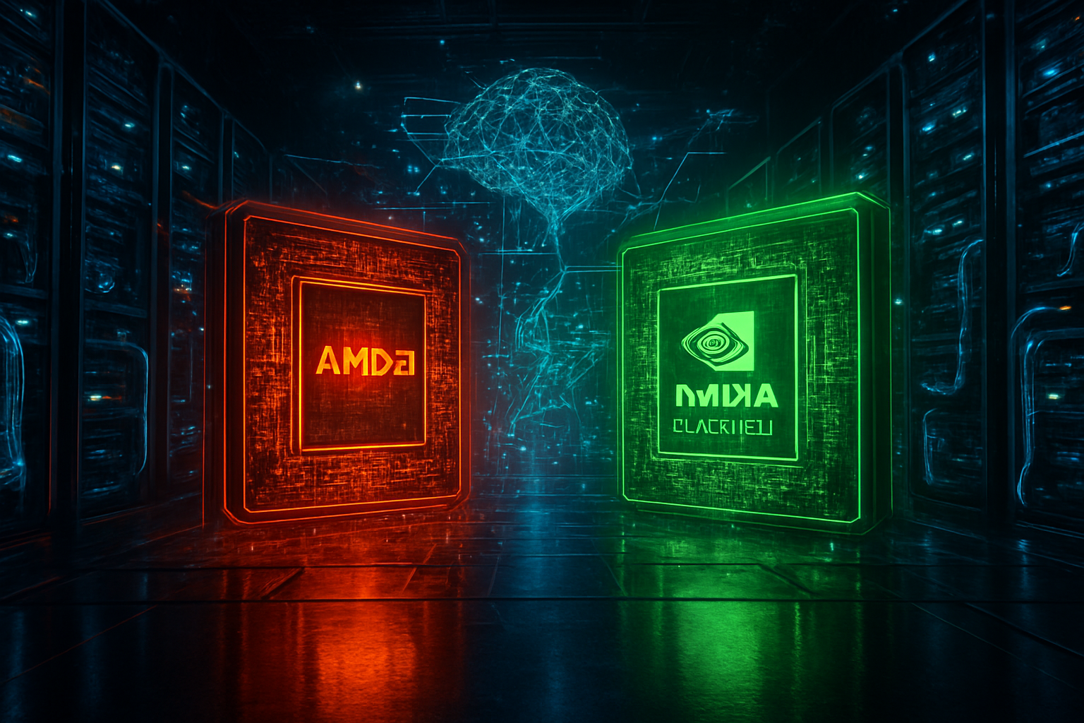
    As of January 2026, the artificial intelligence landscape has transitioned from a period of desperate hardware scarcity to an era of fierce architectural competition. While NVIDIA Corporation (NASDAQ: NVDA) maintained a near-monopoly on high-end AI training for years, the narrative has shifted in the enterprise data center. The arrival of the Advanced Micro Devices, Inc. (NASDAQ: AMD) Instinct MI325X and the subsequent MI350 series has created the first genuine duopoly in the AI accelerator market, forcing a direct confrontation over memory density and inference throughput.

    The immediate significance of this battle lies in the democratization of massive-scale inference. With the release of the MI350 series, built on the cutting-edge 3nm CDNA 4 architecture, AMD has effectively neutralized NVIDIA’s traditional software moat by offering raw hardware specifications—specifically in High Bandwidth Memory (HBM) capacity—that make it mathematically more efficient to run trillion-parameter models on AMD hardware. This shift has prompted major cloud providers and enterprise leaders to diversify their silicon portfolios, ending the "NVIDIA-only" era of the AI boom.

    Technical Superiority through Memory and Precision

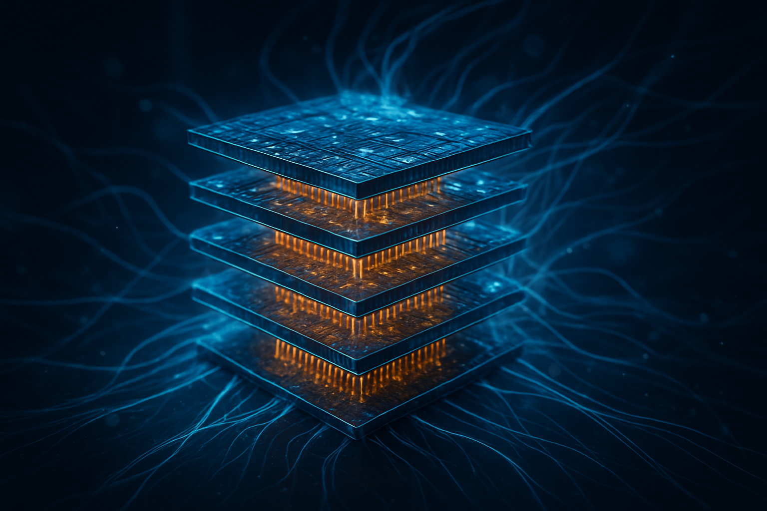
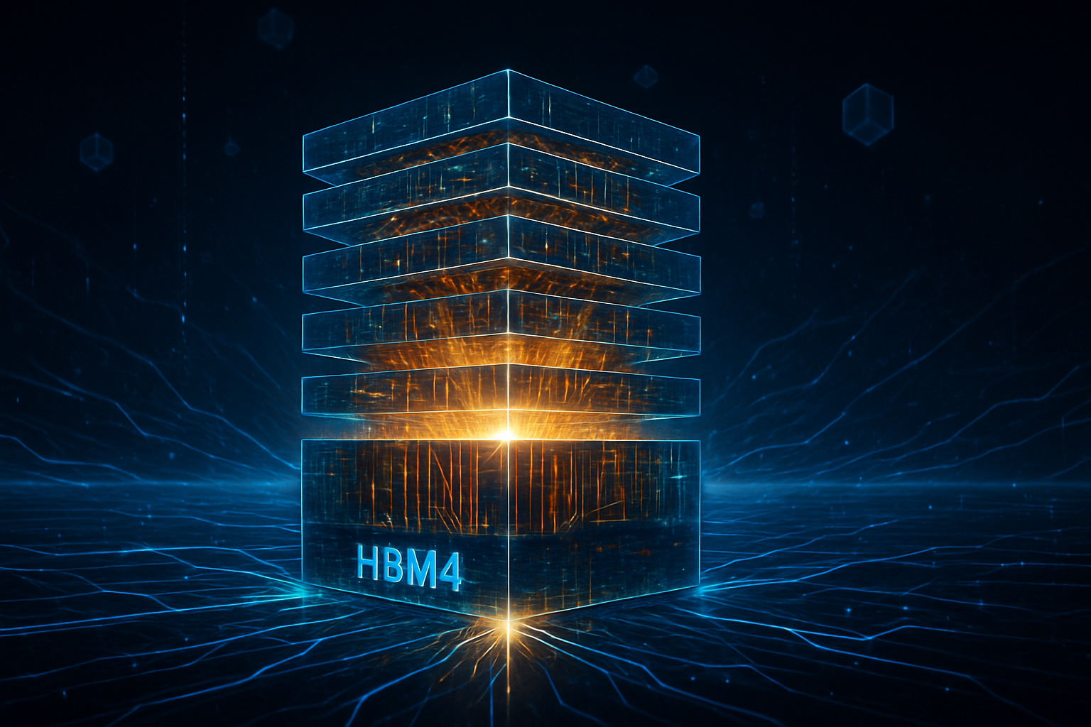
    The technical skirmish between AMD and NVIDIA is currently centered on two critical metrics: HBM3e density and FP4 (4-bit floating point) throughput. The AMD Instinct MI350 series, headlined by the MI355X, boasts a staggering 288GB of HBM3e memory and a peak memory bandwidth of 8.0 TB/s. This allows the chip to house massive Large Language Models (LLMs) entirely within a single GPU's memory, reducing the latency-heavy data transfers between chips that plague smaller-memory architectures. In response, NVIDIA accelerated its roadmap, releasing the Blackwell Ultra (B300) series in late 2025, which finally matched AMD’s 288GB density by utilizing 12-high HBM3e stacks.

    AMD’s generational leap from the MI300 to the MI350 is perhaps the most significant in the company’s history, delivering a 35x improvement in inference performance. Much of this gain is attributed to the introduction of native FP4 support, a precision format that allows for higher throughput without a proportional loss in model accuracy. While NVIDIA’s Blackwell architecture (B200) initially set the gold standard for FP4, AMD’s MI350 has achieved parity in dense compute performance, claiming up to 20 PFLOPS of FP4 throughput. This technical parity has turned the "Instinct vs. Blackwell" debate into a question of TCO (Total Cost of Ownership) rather than raw capability.

    Industry experts initially reacted with skepticism to AMD’s aggressive roadmap, but the mid-2025 launch of the CDNA 4 architecture proved that AMD could maintain a yearly cadence to match NVIDIA’s breakneck speed. The research community has particularly praised AMD’s commitment to open standards via ROCm 7.0. By late 2025, ROCm reached feature parity with NVIDIA’s CUDA for the vast majority of PyTorch and JAX-based workloads, effectively lowering the "switching cost" for developers who were previously locked into NVIDIA’s ecosystem.

    Strategic Realignment in the Enterprise Data Center

    The competitive implications of this hardware parity are profound for the "Magnificent Seven" and emerging AI startups. For companies like Microsoft Corporation (NASDAQ: MSFT) and Meta Platforms, Inc. (NASDAQ: META), the MI350 series provides much-needed leverage in price negotiations with NVIDIA. By deploying thousands of AMD nodes, these giants have signaled that they are no longer beholden to a single vendor. This was most notably evidenced by OpenAI's landmark 2025 deal to utilize 6 gigawatts of AMD-powered infrastructure, a move that provided the MI350 series with the ultimate technical validation.

    For NVIDIA, the emergence of a potent MI350 series has forced a shift in strategy from selling individual GPUs to selling entire "AI Factories." NVIDIA's GB200 NVL72 rack-scale systems remain the industry benchmark for large-scale training due to the superior NVLink 5.0 interconnect, which offers 1.8 TB/s of chip-to-chip bandwidth. However, AMD’s acquisition of ZT Systems, completed in 2025, has allowed AMD to compete at this system level. AMD can now deliver fully integrated, liquid-cooled racks that rival NVIDIA’s DGX systems, directly challenging NVIDIA’s dominance in the plug-and-play enterprise market.

    Startups and smaller enterprise players are the primary beneficiaries of this competition. As NVIDIA and AMD fight for market share, the cost per token for inference has plummeted. AMD has aggressively marketed its MI350 chips as providing "40% more tokens-per-dollar" than the Blackwell B200. This pricing pressure has prevented NVIDIA from further expanding its already record-high margins, creating a more sustainable economic environment for companies building application-layer AI services.

    The Broader AI Landscape: From Scarcity to Scale

    This battle fits into a broader trend of "Inference-at-Scale," where the industry’s focus has shifted from training foundational models to serving them to millions of users efficiently. In 2024, the bottleneck was getting any chips at all; in 2026, the bottleneck is the power density and cooling capacity of the data center. The MI350 and Blackwell Ultra series both push the limits of power consumption, with peak TDPs reaching between 1200W and 1400W. This has sparked a massive secondary industry in liquid cooling and data center power management, as traditional air-cooled racks can no longer support these top-tier accelerators.

    The significance of the 288GB HBM3e threshold cannot be overstated. It marks a milestone where "frontier" models—those with 500 billion to 1 trillion parameters—can be served with significantly less hardware overhead. This reduces the physical footprint of AI data centers and mitigates some of the environmental concerns surrounding AI’s energy consumption, as higher memory density leads to better energy efficiency per inference task.

    However, this rapid advancement also brings concerns regarding electronic waste and the speed of depreciation. With both NVIDIA and AMD moving to annual release cycles, high-end accelerators purchased just 18 months ago are already being viewed as legacy hardware. This "planned obsolescence" at the silicon level is a new phenomenon for the enterprise data center, requiring a complete rethink of how companies amortize their massive capital expenditures on AI infrastructure.

    Looking Ahead: Vera Rubin and the MI400

    The next 12 to 24 months will see the introduction of NVIDIA’s "Vera Rubin" architecture and AMD’s Instinct MI400. Experts predict that NVIDIA will attempt to reclaim its undisputed lead by introducing even more proprietary interconnect technologies, potentially moving toward optical interconnects to overcome the physical limits of copper. NVIDIA is expected to lean heavily into its "Grace" CPU integration, pushing the Superchip model even harder to maintain a system-level advantage that AMD’s MI350, which often relies on third-party CPUs, may struggle to match.

    AMD, meanwhile, is expected to double down on its "chiplet" advantage. The MI400 is rumored to utilize an even more modular design, allowing for customizable ratios of compute to memory. This would allow enterprise customers to order "inference-heavy" or "training-heavy" versions of the same chip, a level of flexibility that NVIDIA’s more monolithic Blackwell architecture does not currently offer. The challenge for both will remain the supply chain; while HBM shortages have eased by early 2026, the sub-3nm fabrication capacity at TSMC remains a tightly contested resource.

    A New Era of Silicon Competition

    The battle between the AMD Instinct MI350 and NVIDIA Blackwell marks the end of the first phase of the AI revolution and the beginning of a mature, competitive industry. NVIDIA remains the revenue leader, holding approximately 85% of the market share, but AMD’s projected climb to a 10-12% share by mid-2026 represents a massive shift in the data center power dynamic. The "GPU War" has successfully moved the needle from theoretical performance to practical, enterprise-grade reliability and cost-efficiency.

    As we move further into 2026, the key metric to watch will be the adoption of these chips in the "sovereign AI" sector—nationalized data centers and regional cloud providers. While the US hyperscalers have led the way, the next wave of growth for both AMD and NVIDIA will come from global markets seeking to build their own independent AI infrastructure. For the first time in the AI era, those customers truly have a choice.


    This content is intended for informational purposes only and represents analysis of current AI developments.

    TokenRing AI delivers enterprise-grade solutions for multi-agent AI workflow orchestration, AI-powered development tools, and seamless remote collaboration platforms.
    For more information, visit https://www.tokenring.ai/.

  • Breaking the Memory Wall: Silicon Photonics Emerges as the Backbone of the Trillion-Parameter AI Era

    Breaking the Memory Wall: Silicon Photonics Emerges as the Backbone of the Trillion-Parameter AI Era

    The rapid evolution of artificial intelligence has reached a critical juncture where the physical limitations of electricity are no longer sufficient to power the next generation of intelligence. For years, the industry has warned of the "Memory Wall"—the bottleneck where data cannot move between processors and memory fast enough to keep up with computation. As of January 2026, a series of breakthroughs in silicon photonics has officially shattered this barrier, transitioning light-based data movement and optical transistors from the laboratory to the core of the global AI infrastructure.

    This "Photonic Pivot" represents the most significant shift in semiconductor architecture since the transition to multi-core processing. By replacing copper wires with laser-driven interconnects and implementing the first commercially viable optical transistors, tech giants and specialized startups are now training trillion-parameter Large Language Models (LLMs) at speeds and energy efficiencies previously deemed impossible. The era of the "planet-scale" computer has arrived, where the distance between chips is no longer measured in centimeters, but in the nanoseconds it takes for a photon to traverse a fiber-optic thread.

    The Dawn of the Optical Transistor: A Technical Leap

    The most striking advancement in early 2026 comes from the miniaturization of optical components. Historically, optical modulators were too bulky to compete with electronic transistors at the chip level. However, in January 2026, the startup Neurophos—heavily backed by Microsoft (NASDAQ: MSFT)—unveiled the Tulkas T100 Optical Processing Unit (OPU). This chip utilizes micron-scale metamaterial optical modulators that function as "optical transistors," measuring nearly 10,000 times smaller than previous silicon photonic elements. This miniaturization allows for a 1000×1000 photonic tensor core capable of delivering 470 petaFLOPS of FP4 compute—roughly ten times the performance of today’s leading GPUs—at a fraction of the power.

    Unlike traditional electronic chips that operate at 2–3 GHz, these photonic processors run at staggering clock speeds of 56 GHz. This speed is made possible by the "Photonic Fabric" technology, popularized by the recent $3.25 billion acquisition of Celestial AI by Marvell Technology (NASDAQ: MRVL). This fabric allows a GPU to access up to 32TB of shared memory across an entire rack with less than 250ns of latency. By treating remote memory pools as if they were physically attached to the processor, silicon photonics has effectively neutralized the memory wall, allowing trillion-parameter models to reside entirely within a high-speed, optically-linked memory space.

    The industry has also moved toward Co-Packaged Optics (CPO), where the laser engines are integrated directly onto the same package as the processor or switch. Intel (NASDAQ: INTC) has led the charge in scalability, reporting the shipment of over 8 million Photonic Integrated Circuits (PICs) by January 2026. Their latest Optical Compute Interconnect (OCI) chiplets, integrated into the Panther Lake AI accelerators, have reduced chip-to-chip latency to under 10 nanoseconds, proving that silicon photonics is no longer a niche technology but a mass-manufactured reality.

    The Industry Reshuffled: Nvidia, Marvell, and the New Hierarchy

    The move to light-based computing has caused a massive strategic realignment among the world's most valuable tech companies. At CES 2026, Nvidia (NASDAQ: NVDA) officially launched its Rubin platform, which marks the company's first architecture to make optical I/O a mandatory requirement. By utilizing Spectrum-X Ethernet Photonics, Nvidia has achieved a five-fold power reduction per 1.6 Terabit (1.6T) port. This move solidifies Nvidia's position not just as a chip designer, but as a systems architect capable of orchestrating million-GPU clusters that operate as a single unified machine.

    Broadcom (NASDAQ: AVGO) has also reached a milestone with its Tomahawk 6-Davisson switch, which began volume shipping in late 2025. Boasting a total capacity of 102.4 Tbps, the TH6 uses 16 integrated optical engines to handle the massive data throughput required by hyperscalers like Meta and Google. For startups, the bar for entry has been raised; companies that cannot integrate photonic interconnects into their hardware roadmaps are finding themselves unable to compete in the high-end training market.

    The acquisition of Celestial AI by Marvell is perhaps the most telling business move of the year. By combining Marvell's expertise in CXL/PCIe protocols with Celestial's optical memory pooling, the company has created a formidable alternative to Nvidia’s proprietary NVLink. This "democratization" of high-speed interconnects allows smaller cloud providers and sovereign AI labs to build competitive training clusters using a mix of hardware from different vendors, provided they all speak the language of light.

    Wider Significance: Solving the AI Energy Crisis

    Beyond the technical specs, the breakthrough in silicon photonics addresses the most pressing existential threat to the AI industry: energy consumption. By mid-2025, the energy demands of global data centers were threatening to outpace national grid capacities. Silicon photonics offers a way out of this "Copper Wall," where the heat generated by pushing electrons through traditional wires became the limiting factor for performance. Lightmatter’s Passage L200 platform, for instance, has demonstrated training times for trillion-parameter models that are up to 8x faster than the 2024 copper-based baseline while reducing interconnect power consumption by over 70%.

    The academic community has also provided proof of a future where AI might not even need electricity for computation. A landmark paper published in Science in December 2025 by researchers at Shanghai Jiao Tong University described the first all-optical computing chip capable of supporting generative models. Similarly, a study in Nature demonstrated "in-situ" training, where neural networks were trained entirely with light signals, bypassing the need for energy-intensive digital-to-analog translations.

    These developments suggest that we are entering an era of "Neuromorphic Photonics," where the hardware architecture more closely mimics the parallel, low-power processing of the human brain. This shift is expected to mitigate concerns about the environmental impact of AI, potentially allowing for the continued exponential growth of model intelligence without the catastrophic carbon footprint previously projected.

    Future Horizons: 3.2T Interconnects and All-Optical Inference

    Looking ahead to late 2026 and 2027, the roadmap for silicon photonics is focused on doubling bandwidth and moving optical computing closer to the edge. Industry insiders expect the announcement of 3.2 Terabit (3.2T) optical modules by the end of the year, which would further accelerate the training of multi-trillion-parameter "World Models"—AIs capable of understanding complex physical environments in real-time.

    Another major frontier is the development of all-optical inference. While training still benefits from the precision of electronic/photonic hybrid systems, the goal is to create inference chips that use almost zero power by processing data purely through light interference. However, significant challenges remain. Packaging these complex "photonic-electronic" hybrids at scale is notoriously difficult, and manufacturing yields for metamaterial transistors need to improve before they can be deployed in consumer-grade devices like smartphones or laptops.

    Experts predict that within the next 24 months, the concept of a "standalone GPU" will become obsolete. Instead, we will see "Opto-Compute Tiles," where processing, memory, and networking are so tightly integrated via photonics that they function as a single continuous fabric of logic.

    A New Era for Artificial Intelligence

    The breakthroughs in silicon photonics documented in early 2026 represent a definitive end to the "electrical era" of high-performance computing. By successfully miniaturizing optical transistors and deploying photonic interconnects at scale, the industry has solved the memory wall and opened a clear path toward artificial general intelligence (AGI) systems that require massive data movement and low latency.

    The significance of this milestone cannot be overstated; it is the physical foundation that will support the next decade of AI innovation. While the transition has required billions in R&D and a total overhaul of data center design, the results are undeniable: faster training, lower energy costs, and the birth of a unified, planet-scale computing architecture. In the coming weeks, watch for the first benchmarks of trillion-parameter models trained on the Nvidia Rubin and Neurophos T100 platforms, which are expected to set new records for both reasoning capability and training efficiency.


    This content is intended for informational purposes only and represents analysis of current AI developments.

    TokenRing AI delivers enterprise-grade solutions for multi-agent AI workflow orchestration, AI-powered development tools, and seamless remote collaboration platforms.
    For more information, visit https://www.tokenring.ai/.

  • Beyond the Shrink: How 6-Micrometer Hybrid Bonding is Resurrecting Moore’s Law for the AI Era

    Beyond the Shrink: How 6-Micrometer Hybrid Bonding is Resurrecting Moore’s Law for the AI Era

    As of early 2026, the semiconductor industry has reached a definitive turning point where the traditional method of scaling—simply making transistors smaller—is no longer the primary driver of computing power. Instead, the focus has shifted to "Advanced Packaging," a sophisticated method of stacking and connecting multiple chips to act as a single, massive processor. At the heart of this revolution is Taiwan Semiconductor Manufacturing Company (NYSE: TSM), whose System on Integrated Chips (SoIC) technology has become the industry standard for bridging the gap between theoretical chip designs and the massive computational demands of generative AI.

    The move to 6-micrometer (6µm) bond pitches represents the current "Goldilocks" zone of semiconductor manufacturing, providing the density required for next-generation AI accelerators like NVIDIA’s (NASDAQ: NVDA) upcoming Rubin architecture and AMD’s (NASDAQ: AMD) Instinct MI400 series. By utilizing hybrid bonding—a process that replaces traditional solder bumps with direct copper-to-copper connections—manufacturers are successfully bypassing the physical limits of monolithic silicon, effectively keeping Moore’s Law alive through vertical integration rather than horizontal shrinkage.

    The Technical Frontier: SoIC and the 6µm Milestone

    TSMC’s SoIC technology represents the pinnacle of 3D heterogeneous integration, specifically through its "bumpless" hybrid bonding technique known as SoIC-X. Unlike traditional 2.5D packaging, which places chips side-by-side on a silicon interposer (such as CoWoS), SoIC-X allows for logic-on-logic stacking. By reducing the bond pitch—the distance between interconnects—to 6 micrometers, TSMC has achieved a 100x increase in interconnect density compared to the 30-40µm pitches used in traditional micro-bump technologies. This leap allows for massive bandwidth between stacked dies, essentially eliminating the latency that usually occurs when data travels between different parts of a processor.

    Technical specifications for the 2026 roadmap indicate that while 6µm is the current high-volume standard, the industry is already testing 4µm and 3µm pitches for late 2026 deployments. This roadmap is critical for the integration of HBM4 (High Bandwidth Memory), which requires these ultra-fine pitches to manage the thermal and electrical signaling of 16-high memory stacks. Initial reactions from the research community have been overwhelmingly positive, with engineers noting that 6µm hybrid bonding allows them to treat separate chiplets as a single "virtual monolithic" die, granting the architectural freedom to mix and match different process nodes (e.g., a 2nm compute die on a 5nm I/O die).

    Market Dynamics: The Battle for AI Supremacy

    The shift toward high-density hybrid bonding has ignited a fierce competitive landscape among chip designers and foundries. NVIDIA (NASDAQ: NVDA) has pivoted its roadmap to take full advantage of TSMC’s SoIC, moving away from the side-by-side Blackwell designs toward the fully 3D-stacked Rubin platform. This move solidifies NVIDIA’s market positioning by allowing it to pack significantly more compute power into the same physical footprint, a necessity for the power-constrained environments of modern data centers. Meanwhile, AMD (NASDAQ: AMD) continues to leverage its early-mover advantage in 3D stacking; having pioneered SoIC with the MI300, it is now utilizing 6µm bonding in the MI400 to maintain its lead in memory capacity and bandwidth.

    However, TSMC is not the only player in this space. Intel (NASDAQ: INTC) is aggressively pushing its Foveros Direct 3D technology, which aims for sub-5µm pitches to support its 18A-PT process node. Intel’s "Clearwater Forest" Xeon processors are the first major test of this technology, positioning the company as a viable alternative for AI companies looking to diversify their supply chains. Samsung (KRX: 005930) is also a major contender with its X-Cube and SAINT platforms. Samsung's unique strategic advantage lies in its "turnkey" capability: it is currently the only company that can manufacture the HBM memory, the logic dies, and the advanced 3D packaging under one roof, potentially lowering costs for hyperscalers like Google or Meta.

    Wider Significance: A New Paradigm for Moore’s Law

    The wider significance of 6µm hybrid bonding cannot be overstated; it represents the shift from the "Era of Shrink" to the "Era of Integration." For decades, Moore's Law relied on the ability to double transistor density on a single piece of silicon every two years. As that process has become exponentially more expensive and physically difficult, advanced packaging has stepped in as the "Silicon Lego" solution. By stacking chips vertically, designers can continue to increase transistor counts without the catastrophic yield losses associated with building giant, monolithic chips.

    This development also addresses the "memory wall"—the bottleneck where processor speed outpaces the speed at which data can be fetched from memory. 3D stacking places memory directly on top of the logic, reducing the distance data must travel and significantly lowering power consumption. However, this transition brings new concerns, primarily regarding thermal management. Stacking high-performance logic dies creates "heat sandwiches" that require innovative cooling solutions, such as microfluidic cooling or advanced diamond-based thermal spreaders, to prevent the chips from throttling or failing.

    The Horizon: Glass Substrates and Sub-3µm Pitches

    Looking ahead, the industry is already identifying the next hurdles beyond 6µm bonding. The next two to three years will likely see the adoption of glass substrates to replace traditional organic materials. Glass offers superior flatness and thermal stability, which is essential as bond pitches continue to shrink toward 2µm and 1µm. Experts predict that by 2028, we will see the first "3.5D" architectures in the wild—complex systems where multiple 3D-stacked logic towers are interconnected on a glass interposer, providing a level of complexity that was unimaginable a decade ago.

    The challenges remaining are primarily economic and logistical. The equipment required for hybrid bonding, such as high-precision wafer-to-wafer aligners, is currently in short supply, and the "cleanliness" requirements for a 6µm bond are far stricter than for traditional packaging. Any microscopic dust particle can ruin a hybrid bond, leading to lower yields. As the industry moves toward these finer pitches, the role of automated inspection and AI-driven quality control will become just as important as the bonding technology itself.

    Conclusion: The 3D Future of Artificial Intelligence

    The transition to 6-micrometer hybrid bonding and TSMC’s SoIC platform marks a definitive end to the "monolithic era" of computing. As of January 30, 2026, the success of the world’s most powerful AI models is now inextricably linked to the success of 3D vertical stacking. By allowing for unprecedented interconnect density and bandwidth, advanced packaging has provided the industry with a second wind, ensuring that the computational gains required for the next phase of AI development remain achievable.

    In the coming months, keep a close eye on the production yields of NVIDIA’s Rubin and the initial benchmarks of Intel’s 18A-PT products. These will serve as the litmus test for whether hybrid bonding can be scaled to the volumes required by the insatiable AI market. While the physical limits of the transistor may be in sight, the architectural possibilities of 3D integration are just beginning to be explored. Moore’s Law isn’t dead; it has simply moved into the third dimension.


    This content is intended for informational purposes only and represents analysis of current AI developments.

    TokenRing AI delivers enterprise-grade solutions for multi-agent AI workflow orchestration, AI-powered development tools, and seamless remote collaboration platforms.
    For more information, visit https://www.tokenring.ai/.

  • The Silicon Standoff: China’s Strategic Pivot and the New Geopolitical Tax on NVIDIA’s AI Dominance

    The Silicon Standoff: China’s Strategic Pivot and the New Geopolitical Tax on NVIDIA’s AI Dominance

    As of late January 2026, the global semiconductor industry has entered a volatile new chapter. Following years of tightening export controls, a complex "revenue-for-access" truce has emerged between Washington and Beijing, fundamentally altering the strategic calculus for NVIDIA Corporation (NASDAQ: NVDA). While recent regulatory shifts have nominally reopened the door for NVIDIA’s high-performance H200 chips, the landscape they return to is no longer a monopoly. China’s major technology conglomerates—once NVIDIA’s most reliable customers—are increasingly rejecting "downgraded" western silicon in favor of domestic self-sufficiency.

    This pivot represents a watershed moment in the AI arms race. The rejection of NVIDIA’s previous "China-specific" offerings, such as the H20, has forced a recalibration of the entire regional revenue strategy for the Santa Clara-based giant. As Chinese firms like Alibaba Group Holding Ltd. (NYSE: BABA) and Tencent Holdings Ltd. (HKG: 0700) accelerate their transition to homegrown architectures, the global AI supply chain is bifurcating into two distinct, and increasingly incompatible, ecosystems.

    The technical catalyst for this shift lies in the stark performance gap of previous "compliant" chips. Throughout 2025, NVIDIA attempted to navigate U.S. Department of Commerce restrictions by offering the H20, a modified version of its Hopper architecture with significantly throttled processing power. Research indicates the H20 delivered roughly 40% of the compute density of the flagship H100, a deficit that rendered it nearly useless for training the next generation of frontier Large Language Models (LLMs). This performance "floor" became a breaking point; by late 2025, Chinese cloud providers began canceling massive H20 orders, citing an inability to remain competitive with Western AI labs using unencumbered hardware.

    In response, the market has seen the rise of legitimate domestic rivals, most notably Huawei’s Ascend 910C. As of January 2026, the 910C has become the benchmark for Chinese AI compute, offering system-level innovations such as the CloudMatrix 384—a clustered architecture designed to rival NVIDIA’s high-bandwidth interconnects. While the individual H200 chip still maintains a roughly 32% processing advantage over the 910C, Huawei has narrowed the gap significantly in memory bandwidth and vertical software integration via its CANN (Compute Architecture for Neural Networks) framework. This progress has empowered Chinese firms to take a "dual-track" approach: utilizing NVIDIA's H200 for the most intensive training phases while shifting the bulk of their inference and mid-tier training to domestic hardware.

    The competitive implications of this shift are profound for the world's leading chipmakers. For NVIDIA, the China market—which historically accounted for up to 25% of total revenue—plummeted to mid-single digits in late 2025 before the recent "case-by-case" review policy for the H200 was enacted on January 15, 2026. While analysts project this opening could unlock a $40 billion to $50 billion annual opportunity, it comes with a heavy "geopolitical tax." Under the new "Trump-Huang Revenue Model," a 25% value-based tariff is now imposed on every advanced AI chip exported to China, with proceeds directed to the U.S. Treasury. This policy creates an unprecedented scenario where NVIDIA must manage record-high demand while facing significant pressure on net profit margins.

    Beyond NVIDIA, the ripples are felt by Advanced Micro Devices, Inc. (NASDAQ: AMD) and Intel Corporation (NASDAQ: INTC), both of whom are struggling to secure similar "green light" status for their high-end accelerators like the MI325X. Meanwhile, the biggest beneficiaries of this tension are domestic Chinese semiconductor players. Semiconductor Manufacturing International Corporation (SHA: 601238), or SMIC, has seen a surge in orders as it refines its 7nm and 5nm-class processes to support Huawei’s ramping production. The emergence of Alibaba’s internal chip unit, T-Head, and its Zhenwu 810E processor, further illustrates how tech giants are pivoting from being NVIDIA’s customers to becoming its primary regional competitors.

    On a broader scale, this development signals the official end of a unified global AI stack. The "50% domestic equipment rule" reportedly implemented by Chinese regulators in late 2025 mandates that state-funded and even some private data centers must source half of their hardware locally. This policy serves as a protective barrier, ensuring that even as NVIDIA regains access to the market, domestic players like Huawei and Cambricon Technologies (SHA: 688256) are guaranteed a significant market share. This is AI sovereignty in action—a direct response to years of U.S. sanctions that have convinced Beijing that reliance on Western silicon is a terminal risk.

    The geopolitical landscape of 2026 is now defined by what experts call the "Silicon Splinternet." The U.S. strategy has shifted from a total blockade to a tactical "locking in" effect. By allowing the H200 back into the market under heavy tariffs, the U.S. aims to keep Chinese developers tethered to NVIDIA’s CUDA software ecosystem, preventing a total migration to Huawei’s alternative frameworks. This is a delicate balancing act; too much restriction accelerates Chinese innovation, while too little allows China to reach parity with Western AI capabilities. The current status quo is a high-stakes compromise where innovation is effectively taxed to fund national security.

    Looking ahead, the next twelve to eighteen months will be defined by the race to the "post-Hopper" era. NVIDIA is already preparing its Blackwell-based (B20/B30A) offerings for the Chinese market, which will likely face even stricter scrutiny and higher tariffs. Simultaneously, the focus is shifting to the upcoming "Rubin" architecture, slated for late 2026. Experts predict that the battleground will move from raw compute power to the "interconnect war," as Chinese firms attempt to replicate NVIDIA’s NVLink technology to overcome the limitations of individual chip performance through massive, efficient clusters.

    However, significant hurdles remain for China's domestic ambitions. Yield rates at SMIC and the ongoing struggle to secure advanced Lithography equipment continue to plague the mass production of the Ascend 910C and 910D. Furthermore, the transition from CUDA to domestic software stacks remains a "painful and buggy" process for developers, as evidenced by the technical setbacks faced by AI startup DeepSeek during its recent training cycles. The coming months will determine if the current "dual-track" strategy is a temporary bridge or a permanent divorce from the Western supply chain.

    The "Silicon Standoff" of 2026 marks a definitive turning point in the history of the semiconductor industry. NVIDIA remains the undisputed king of performance, but its crown is being increasingly weighed down by the heavy machinery of international diplomacy. The rejection of the H20 and the cautious, tariff-laden adoption of the H200 demonstrate that in the modern era, a chip’s technical specifications are only as valuable as the geopolitical permissions attached to them.

    As we move deeper into 2026, the industry must watch two critical indicators: the success of Huawei’s next-gen 910D production and the sustainability of the 25% "AI tariff" model. If Chinese firms can successfully migrate their LLM training to domestic hardware without a significant loss in intelligence, the "NVIDIA era" in the East may be nearing its conclusion. For now, the world remains in a state of watchful tension, where every transistor shipped across the Pacific is a move in a global game of chess.


    This content is intended for informational purposes only and represents analysis of current AI developments.

    TokenRing AI delivers enterprise-grade solutions for multi-agent AI workflow orchestration, AI-powered development tools, and seamless remote collaboration platforms.
    For more information, visit https://www.tokenring.ai/.

  • SK Hynix Invests $13 Billion in World’s Largest HBM Packaging Plant (P&T7) to Power NVIDIA’s Rubin Era

    SK Hynix Invests $13 Billion in World’s Largest HBM Packaging Plant (P&T7) to Power NVIDIA’s Rubin Era

    In a move that solidifies its lead in the high-stakes artificial intelligence memory race, SK Hynix (KRX: 000660) has officially announced a massive $13 billion (19 trillion won) investment to construct "P&T7," slated to be the world's largest dedicated High Bandwidth Memory (HBM) packaging and testing facility. Located in the Cheongju Technopolis Industrial Complex in South Korea, this facility is designed to serve as the global nerve center for the production of HBM4, the next-generation memory architecture required to power the most advanced AI processors on the planet.

    The announcement, formalized on January 13, 2026, marks a pivotal moment in the semiconductor industry as the demand for memory bandwidth begins to outpace traditional compute scaling. By integrating the P&T7 facility with the adjacent M15X production line, SK Hynix is creating a vertically integrated "super-fab" capable of handling everything from initial DRAM fabrication to the complex 16-layer vertical stacking required for NVIDIA (NASDAQ: NVDA) and its upcoming Rubin GPU architecture. This investment signals that the bottleneck for AI progress is no longer just the logic of the chip, but the speed and efficiency with which that chip can access data.

    The Technical Frontier: HBM4 and the Logic-Memory Merger

    The P&T7 facility is specifically engineered to overcome the daunting physical challenges of HBM4. Unlike its predecessor, HBM3E, which featured a 1024-bit interface, HBM4 doubles the interface width to 2048-bit. This leap allows for staggering bandwidths exceeding 2 TB/s per memory stack. To achieve this, SK Hynix is deploying its proprietary Advanced Mass Reflow Molded Underfill (MR-MUF) technology at P&T7. This process allows the company to stack up to 16 layers of DRAM—offering capacities of 64GB per cube—while keeping the total height within the strict 775-micrometer JEDEC standard. This requires thinning individual DRAM dies to a mere 30 micrometers, a feat of precision engineering that P&T7 is uniquely equipped to handle at scale.

    Perhaps the most significant technical shift at P&T7 is the transition of the HBM "base die." In previous generations, the base die was a standard memory component. For HBM4, the base die will be manufactured using advanced logic processes (5nm and 3nm) in collaboration with TSMC (NYSE: TSM). This effectively turns the memory stack into a semi-custom co-processor, allowing for better thermal management and lower latency. The P&T7 plant will act as the final integration point where these TSMC-made logic dies are married to SK Hynix’s high-density DRAM, representing an unprecedented level of cross-foundry collaboration.

    Initial reactions from the semiconductor research community suggest that SK Hynix’s decision to stick with MR-MUF for the initial 16-layer HBM4 rollout—rather than jumping immediately to hybrid bonding—is a strategic move to ensure high yields. While competitors are experimenting with hybrid bonding to reduce stack height, SK Hynix’s refined MR-MUF process has already demonstrated superior thermal dissipation, a critical factor for GPUs like NVIDIA’s Blackwell and Rubin that operate at extreme power densities.

    Securing the NVIDIA Pipeline: From Blackwell to Rubin

    The primary beneficiary of this $13 billion investment is NVIDIA (NASDAQ: NVDA), which has reportedly secured approximately 70% of SK Hynix's HBM4 production capacity through 2027. While SK Hynix currently dominates the supply of HBM3E for the NVIDIA Blackwell (B100/B200) family, the P&T7 facility is built with the future "Rubin" platform in mind. The Rubin GPU is expected to utilize eight stacks of HBM4, providing an astronomical 288GB of ultra-fast memory and 22 TB/s of bandwidth. This leap is essential for the next generation of LLMs, which are expected to exceed 10 trillion parameters.

    The competitive implications for other tech giants are profound. Samsung (KRX: 005930) and Micron (NASDAQ: MU) are racing to catch up, with Samsung recently passing quality tests for its own HBM4 modules. However, the sheer scale of the P&T7 facility gives SK Hynix a massive advantage in "economies of skill." By housing packaging and testing in such close proximity to the M15X fab, SK Hynix can achieve yield stabilities that are difficult for competitors with fragmented supply chains to match. For hyperscalers like Microsoft (NASDAQ: MSFT) and Meta (NASDAQ: META), who are increasingly designing their own AI silicon, SK Hynix’s P&T7 offers a blueprint for how "custom memory" will be delivered in the late 2020s.

    This investment also disrupts the traditional vendor-client relationship. The move toward logic-based base dies means SK Hynix is moving up the value chain, acting more like a boutique foundry for high-performance components rather than a bulk commodity memory supplier. This strategic positioning makes them an indispensable partner for any company attempting to compete at the frontier of AI training and inference.

    The Broader AI Landscape: Overcoming the Memory Wall

    The P&T7 announcement is a direct response to the "Memory Wall"—the growing disparity between how fast a processor can compute and how fast data can be moved into that processor. As AI models grow in complexity, the energy cost of moving data often exceeds the cost of the computation itself. By doubling the bandwidth and increasing the density of HBM4, SK Hynix is effectively extending the lifespan of current transformer-based AI architectures. Without this $13 billion infrastructure, the industry would likely face a hard ceiling on model performance within the next 24 months.

    Furthermore, this development highlights the shifting center of gravity in the semiconductor supply chain. While much of the world's focus remains on front-end wafer fabrication in Taiwan, the "back-end" of advanced packaging has become the new bottleneck. SK Hynix’s decision to build the world's largest packaging plant in South Korea—while also expanding into West Lafayette, Indiana—shows a sophisticated "hub-and-spoke" strategy to balance geopolitical security with manufacturing efficiency. It places South Korea at the absolute heart of the AI revolution, making the Cheongju Technopolis as vital to the global economy as any logic fab in Hsinchu.

    Comparing this to previous milestones, the P&T7 investment is being viewed by many as the "Gigafactory moment" for the memory industry. Just as massive battery plants were required to make electric vehicles viable, these massive packaging hubs are the prerequisite for the next stage of the AI era. The concern, however, remains one of concentration; with SK Hynix holding such a dominant position in HBM4, any supply chain disruption at the P&T7 site could theoretically stall global AI development for months.

    Looking Ahead: The Road to Rubin Ultra and Beyond

    Construction of the P&T7 facility is scheduled to begin in April 2026, with full-scale operations targeted for late 2027. In the near term, SK Hynix will use interim lines and its existing M15X facility to supply the first wave of HBM4 samples to NVIDIA and other tier-one customers. The industry is closely watching for the transition to "Rubin Ultra," a planned refresh of the Rubin architecture that will likely push HBM4 to 20-layer stacks. Experts predict that P&T7 will be the first facility to pilot hybrid bonding at scale for these 20-layer variants, as the physical limits of MR-MUF are eventually reached.

    Beyond just GPUs, the high-density memory produced at P&T7 is expected to find its way into high-performance computing (HPC) and even specialized "AI PCs" that require massive local bandwidth for on-device inference. The challenge for SK Hynix will be managing the capital expenditure of such a massive project while the memory market remains notoriously cyclical. However, the "AI-driven" cycle appears to have different dynamics than the traditional PC or smartphone cycles, with demand remaining resilient even in fluctuating economic conditions.

    A New Era for AI Hardware

    The $13 billion investment in P&T7 is more than just a factory announcement; it is a declaration of dominance. SK Hynix is betting that the future of AI belongs to the company that can most efficiently package and move data. By securing a 70% stake in NVIDIA’s HBM4 orders and building the infrastructure to support the Rubin architecture, SK Hynix has effectively anchored its position as the primary architect of the AI hardware landscape for the remainder of the decade.

    Key takeaways from this development include the transition of memory from a commodity to a semi-custom logic-integrated component and the critical role of South Korea as a global hub for advanced packaging. As construction begins this spring, the tech world will be watching P&T7 as the ultimate barometer for the health and velocity of the AI boom. In the coming months, expect to see further announcements regarding the deep integration between SK Hynix, NVIDIA, and TSMC as they finalize the specifications for the first production-ready HBM4 modules.


    This content is intended for informational purposes only and represents analysis of current AI developments.

    TokenRing AI delivers enterprise-grade solutions for multi-agent AI workflow orchestration, AI-powered development tools, and seamless remote collaboration platforms.
    For more information, visit https://www.tokenring.ai/.

  • Silicon’s New Horizon: TSMC Hits 2nm Milestone as GAA Transition Reshapes AI Hardware

    Silicon’s New Horizon: TSMC Hits 2nm Milestone as GAA Transition Reshapes AI Hardware

    As of January 30, 2026, the global semiconductor landscape has officially entered the "Angstrom Era." Taiwan Semiconductor Manufacturing Company (NYSE: TSM), the world's largest contract chipmaker, has successfully transitioned its 2nm (N2) process from pilot lines to high-volume manufacturing (HVM). This milestone represents more than just a reduction in feature size; it marks the most significant architectural overhaul in semiconductor design since the introduction of FinFET over a decade ago.

    The immediate significance of the N2 node cannot be overstated, particularly for the burgeoning artificial intelligence sector. With production now scaling at TSMC's Baoshan and Kaohsiung facilities, the first wave of 2nm-powered devices is expected to hit the market by the end of the year. This shift provides the critical hardware foundation required to sustain the massive compute demands of next-generation large language models and autonomous systems, effectively extending the lifespan of Moore’s Law through sheer architectural ingenuity.

    The Nanosheet Revolution: Engineering the 2nm Breakthrough

    The technical centerpiece of the N2 node is the transition from the long-standing FinFET (Fin Field-Effect Transistor) architecture to Gate-All-Around (GAA) technology, which TSMC refers to as "Nanosheet" transistors. In previous FinFET designs, the gate covered three sides of the channel. However, as transistors shrunk toward the 2nm limit, electron leakage became an insurmountable hurdle. The Nanosheet design solves this by wrapping the gate entirely around the channel on all four sides. This provides superior electrostatic control, virtually eliminating current leakage and allowing for significantly lower operating voltages.

    Beyond the transistor geometry, TSMC has introduced a proprietary feature known as NanoFlex™. This technology allows chip designers at firms like Apple (NASDAQ: AAPL) and NVIDIA (NASDAQ: NVDA) to mix and match different standard cell types—short cells for power efficiency and tall cells for peak performance—on a single die. This granular control over the power-performance-area (PPA) profile is unprecedented. Early reports from January 2026 indicate that TSMC has achieved logic test chip yields between 70% and 80%, a remarkable feat that places them well ahead of competitors like Samsung (KRX: 005930), whose 2nm GAA yields are reportedly struggling in the 40-55% range.

    In terms of raw performance, the N2 process is delivering a 10% to 15% speed increase at the same power level compared to the refined 3nm (N3E) process. Perhaps more importantly for mobile and edge AI applications, it offers a 25% to 30% reduction in power consumption at the same clock speed. This efficiency gain is the primary driver for the massive industry interest, as it allows for more complex AI processing to occur on-device without devastating battery life or thermal envelopes.

    The 2026 Capacity Crunch: Apple and NVIDIA Lead the Charge

    The scramble for 2nm capacity has created a "supply choke" that has defined the early months of 2026. Industry insiders confirm that TSMC’s N2 capacity is effectively fully booked through the end of the year, with Apple and NVIDIA emerging as the dominant stakeholders. Apple has reportedly secured over 50% of the initial 2nm output, which it plans to utilize for its upcoming A20 Bionic chips in the iPhone 18 series and the M6 series processors for its MacBook Pro and iPad Pro lineups. For Apple, this exclusivity ensures that its "Apple Intelligence" ecosystem remains the gold standard for on-device AI performance.

    NVIDIA has also made an aggressive play for 2nm wafers to power its "Rubin" GPU platform. As generative AI workloads continue to grow exponentially, NVIDIA’s move to 2nm is seen as a strategic necessity to maintain its dominance in the data center. By moving to the N2 node, NVIDIA can pack more CUDA cores and specialized AI accelerators into a single chip while staying within the power limits of modern liquid-cooled server racks. This has placed smaller AI startups and rival chipmakers in a precarious position, as they must compete for the remaining "leftover" capacity or wait for the 2nm ramp-up to reach 140,000 wafers per month by late 2026.

    The cost of this technological edge is steep. Wafers for the 2nm process are currently estimated at $30,000 each, a 20% premium over the 3nm generation. This pricing reinforces a "winners-take-all" market dynamic, where only the wealthiest tech giants can afford the most advanced silicon. For consumers, this likely translates to higher price points for flagship hardware, but for the industry, it represents the massive capital expenditure required to keep the AI revolution moving forward.

    Redefining the AI Landscape: Sustainability and Sovereignty

    The shift to 2nm has implications that reach far beyond faster smartphones. In the broader AI landscape, the improved power efficiency of N2 is a critical component of the industry’s "green AI" initiatives. As data centers consume an ever-increasing percentage of global electricity, the 30% power reduction offered by 2nm chips becomes a vital tool for sustainability. This allows major cloud providers to expand their AI training clusters without requiring a linear increase in energy infrastructure, mitigating some of the environmental concerns surrounding the AI boom.

    Furthermore, the 2nm milestone solidifies TSMC’s role as the indispensable lynchpin of the global digital economy. As the only foundry currently capable of delivering high-yield 2nm GAA wafers at scale, TSMC’s technological lead has become a matter of national and corporate sovereignty. This has intensified the competitive pressure on Intel (NASDAQ: INTC) and Samsung to accelerate their own roadmaps. While Intel’s 18A process is beginning to gain traction, TSMC’s successful N2 rollout in early 2026 suggests that the "Taiwan Advantage" remains firmly in place for the foreseeable future.

    However, the concentration of 2nm manufacturing in Taiwan remains a point of strategic anxiety for global markets. Despite TSMC’s expansion into Arizona and Japan, the most advanced 2nm "GigaFabs" are currently concentrated in Hsinchu and Kaohsiung. This geopolitical reality means that any disruption in the region would immediately halt the production of the world’s most advanced AI and consumer chips, a vulnerability that continues to drive investments in domestic chip manufacturing in the U.S. and Europe.

    The Road to 1.6nm: Super PowerRail and the A16 Era

    Even as N2 production ramps up, TSMC is already looking toward its next major leap: the A16 (1.6nm) node. Scheduled for high-volume manufacturing in the second half of 2026, A16 will introduce "Super PowerRail" (SPR) technology. This is TSMC’s proprietary implementation of a Backside Power Delivery Network (BSPDN). Traditionally, power and signal lines are bundled on the front side of a wafer. SPR moves the power delivery to the back, connecting it directly to the transistor's source and drain.

    This innovation is expected to free up nearly 20% more space for signal routing on the front side, significantly reducing "IR drop" (voltage loss) and improving power delivery efficiency. Experts predict that A16 will provide an additional 8% to 10% speed boost over N2P (the performance-enhanced version of 2nm). However, moving the power network to the backside presents a new set of thermal management challenges, as the chip's ability to spread heat laterally is reduced. This will likely necessitate new cooling solutions, such as microfluidic channels integrated directly into the chip packaging.

    Looking ahead, the successful deployment of Super PowerRail in the A16 process will be the defining technical challenge of 2027. If TSMC can solve the thermal hurdles associated with backside power, it will pave the way for chips that are not only smaller but fundamentally more efficient at handling the high-intensity, continuous compute required for real-time AI reasoning and 8K holographic rendering.

    Conclusion: A New Era of Silicon Dominance

    TSMC’s 2nm production milestone is a watershed moment in the history of computing. By successfully navigating the transition from FinFET to Nanosheet architecture, the company has provided the world’s leading technology companies with the tools needed to push AI beyond current limitations. The fact that 2026 capacity is already spoken for by Apple and NVIDIA underscores the desperate industry-wide need for more efficient, more powerful silicon.

    As we move through the first quarter of 2026, the key metrics to watch will be the continued stabilization of N2 yields and the first real-world benchmarks from 2nm-equipped devices. While the A16 roadmap and Super PowerRail technology promise even greater gains, the current focus remains on the flawless execution of N2. For the AI industry, the message is clear: the hardware bottleneck is widening, but the price of entry into the elite tier of performance has never been higher. TSMC's achievement ensures that the momentum of the AI era continues unabated, firmly establishing the 2nm node as the backbone of the next generation of digital innovation.


    This content is intended for informational purposes only and represents analysis of current AI developments.

    TokenRing AI delivers enterprise-grade solutions for multi-agent AI workflow orchestration, AI-powered development tools, and seamless remote collaboration platforms.
    For more information, visit https://www.tokenring.ai/.

  • NVIDIA Shatters Records with $57B Quarterly Revenue as Blackwell Ultra Demand Reaches “Off the Charts” Levels

    NVIDIA Shatters Records with $57B Quarterly Revenue as Blackwell Ultra Demand Reaches “Off the Charts” Levels

    In a financial performance that has stunned even the most bullish Wall Street analysts, NVIDIA (NASDAQ: NVDA) has reported a staggering $57 billion in revenue for the third quarter of its fiscal year 2026. This milestone, primarily driven by a 66% year-over-year surge in its Data Center division, underscores an insatiable global appetite for artificial intelligence compute. CEO Jensen Huang described the current market environment as having demand that is "off the charts," as the world’s largest tech entities and specialized AI cloud providers race to secure the latest Blackwell Ultra architecture.

    The immediate significance of this development cannot be overstated. As of January 30, 2026, NVIDIA has effectively solidified its position not just as a chipmaker, but as the primary architect of the global AI economy. The $57 billion quarterly figure—which puts the company on a trajectory to exceed a $250 billion annual run-rate—indicates that the transition from general-purpose computing to accelerated computing is accelerating rather than plateauing. With cloud GPUs currently "sold out" across major providers, the industry is entering a period where the primary constraint on AI progress is no longer algorithmic innovation, but the physical delivery of silicon and power.

    The Blackwell Ultra Era: Technical Dominance and the One-Year Cycle

    The cornerstone of this fiscal triumph is the Blackwell Ultra (B300) architecture, which has rapidly become the flagship product for NVIDIA’s data center customers. Unlike previous generations that followed a two-year release cadence, the Blackwell Ultra represents NVIDIA’s strategic shift to a "one-year release cycle." Technically, the B300 is a significant leap over the initial Blackwell B200 units, featuring an unprecedented 288GB of HBM3e (High Bandwidth Memory) and enhanced throughput via NVLink 5. This allows for the training of larger Mixture-of-Experts (MoE) models with significantly fewer GPUs, drastically reducing the total cost of ownership for massive-scale AI clusters.

    The technical specifications of the Blackwell Ultra systems have fundamentally altered data center design. A single Blackwell rack can now consume up to 120kW of power, necessitating a widespread industry move toward liquid cooling solutions. This shift has created a secondary market boom for infrastructure providers capable of retrofitting legacy air-cooled data centers. Research communities have noted that the B300's ability to handle inference and training on a single, unified architecture has simplified the AI development pipeline, allowing researchers to move from model training to production deployment with minimal latency and reconfiguration.

    Industry experts have expressed awe at the execution of this ramp-up. Despite the complexity of the Blackwell architecture, NVIDIA has managed to scale production while simultaneously readying its next platform. However, the sheer volume of demand has created a massive backlog. Analysts estimate a $500 billion booking pipeline for Blackwell and the upcoming Rubin systems extending through the end of calendar year 2026. This backlog is compounded by extreme tightness in the supply of HBM3e and advanced CoWoS (Chip-on-Wafer-on-Substrate) packaging from partners like TSMC (NYSE: TSM).

    Market Dynamics: Hyperscalers and the "Fairwater" Superfactories

    The primary beneficiaries of the Blackwell Ultra surge are the "hyperscalers"—Microsoft (NASDAQ: MSFT), Alphabet (NASDAQ: GOOGL), Meta (NASDAQ: META), and Amazon (NASDAQ: AMZN). These giants have pre-booked the lion's share of NVIDIA’s 2026 capacity, effectively creating a high barrier to entry for smaller competitors. Microsoft, in particular, has made waves with its "Fairwater" AI superfactory design, which is specifically engineered to house hundreds of thousands of NVIDIA’s high-power Blackwell and future Rubin Superchips. This strategic hoarding of compute power has forced smaller AI labs and startups to rely on specialized cloud providers like CoreWeave, which have secured early-access slots in NVIDIA’s shipping schedule.

    Competitive implications are profound. As NVIDIA’s Blackwell Ultra becomes the industry standard, traditional CPU-centric server architectures from competitors are being rapidly displaced. While companies like Intel (NASDAQ: INTC) and AMD (NASDAQ: AMD) are attempting to gain ground with their own AI accelerators, NVIDIA’s "full stack" approach—incorporating networking via Mellanox and software via the CUDA platform—has created a formidable moat. The strategic advantage for a company like Meta, which uses Blackwell clusters to power its Llama-4 and Llama-5 training runs, is measured in months of lead time over rivals who lack similar access to compute.

    The disruption extends beyond hardware. The massive capital expenditure (CapEx) required to build these AI clusters is reshaping the balance sheets of the world’s largest corporations. With Microsoft and Google reporting record CapEx to keep pace with the Blackwell roadmap, the tech industry is essentially betting its future on the continued scaling of AI capabilities. This has led to a market positioning where "compute-rich" companies are pulling away from "compute-poor" firms, creating a new digital divide in the enterprise sector.

    The Broader AI Landscape: Power, Policy, and Scaling Laws

    As we look at the wider significance of NVIDIA's $57 billion milestone, the primary concern has shifted from silicon availability to energy availability. The broader AI landscape is now grappling with the reality that the next generation of models will require gigawatt-scale power installations. This has sparked a renewed focus on nuclear energy and modular reactors, as the 120kW power density of Blackwell Ultra racks pushes traditional electrical grids to their limits. The environmental impact of this compute explosion is a growing topic of debate, even as NVIDIA argues that accelerated computing is inherently more energy-efficient than traditional methods for the same amount of work.

    Ethically and politically, NVIDIA’s dominance has placed it at the center of national security discussions. The Blackwell Ultra is subject to rigorous export controls, particularly concerning high-end AI chips reaching geopolitical rivals. This has turned GPU allocation into a form of "silicon diplomacy," where access to the latest NVIDIA architecture is seen as a vital national interest. The current milestone is often compared to the 2023 "H100 boom," but the scale is now an order of magnitude larger, indicating that the AI revolution is moving into its heavy-industry phase.

    Furthermore, the "scaling laws"—the observation that more data and more compute lead to more capable AI—remain the guiding light of the industry. NVIDIA’s performance is a direct reflection of the fact that none of the major AI labs have hit a point of diminishing returns. As long as adding more Blackwell Ultra GPUs results in smarter, more capable models, the demand is expected to remain "off the charts," potentially lasting through the end of the decade.

    Looking Ahead: The Transition to the Rubin Platform

    Even as Blackwell Ultra dominates the current discourse, NVIDIA is already preparing for its next major leap: the Rubin platform. Announced in more detail at CES 2026, the Rubin architecture (codenamed Vera Rubin) is slated for production in late 2025 with mass availability expected in the second half of calendar year 2026. The Rubin R100 GPU will be manufactured on a 3nm-class process node and will represent a definitive shift to HBM4 memory technology, offering bandwidth up to 13 TB/s.

    The Rubin platform will also introduce the "Vera" CPU, designed to work in tandem with the R100 GPU as a "Superchip." Experts predict that this platform will deliver a 10x reduction in inference token costs, potentially making real-time, high-reasoning AI applications affordable for the mass market. However, the transition will not be without challenges. The move to HBM4 will require another massive shift in packaging and supply chain logistics, and the industry will once again have to solve the "power wall" as the Vera Rubin chips push energy requirements even higher.

    The near-term future will see a dual-track strategy: the continued rollout of Blackwell Ultra to fill the existing $500 billion backlog, and the early seeding of Rubin-based systems to elite partners. Companies like CoreWeave and Microsoft are already designing data centers for 2027 that can accommodate the "Vera Rubin" era, suggesting that the cycle of rapid-fire hardware releases is the new normal for the foreseeable future.

    Conclusion: A New Chapter in Computing History

    NVIDIA’s fiscal 2026 performance marks a watershed moment in the history of technology. By reaching a $57 billion quarterly revenue milestone, the company has proven that the AI era is not a bubble, but a fundamental restructuring of the global economy around intelligence as a service. The "off the charts" demand for Blackwell Ultra proves that we are in the midst of a massive infrastructure build-out comparable to the construction of the railroads or the electrical grid in previous centuries.

    As we move toward the end of fiscal 2026, the significance of NVIDIA’s dominance is clear: they are the sole provider of the "industrial engine" of the 21st century. While supply constraints and power requirements remain significant hurdles, the momentum behind the Blackwell Ultra and the upcoming Rubin platform suggests that NVIDIA’s lead is, for now, unassailable.

    In the coming weeks and months, all eyes will be on NVIDIA’s Q4 fiscal 2026 earnings report, scheduled for February 25, 2026. With guidance pointing toward $65 billion, the world will be watching to see if NVIDIA can once again exceed its own record-breaking expectations. For the tech industry, the message is clear: the age of accelerated computing is here, and it is powered by Blackwell.


    This content is intended for informational purposes only and represents analysis of current AI developments.

    TokenRing AI delivers enterprise-grade solutions for multi-agent AI workflow orchestration, AI-powered development tools, and seamless remote collaboration platforms.
    For more information, visit https://www.tokenring.ai/.

  • Japan’s FugakuNEXT Revolution: RIKEN Deploys Liquid-Cooled NVIDIA Blackwell to Bridge Quantum and AI

    Japan’s FugakuNEXT Revolution: RIKEN Deploys Liquid-Cooled NVIDIA Blackwell to Bridge Quantum and AI

    In a landmark announcement this January 2026, the RIKEN Center for Computational Science (R-CCS) has officially selected NVIDIA (NASDAQ:NVDA) Grace Blackwell architectures to power the developmental stages of "FugakuNEXT," the highly anticipated successor to the world-renowned Fugaku supercomputer. This strategic move signals a paradigm shift in Japan’s high-performance computing (HPC) strategy, moving away from a purely classical CPU-centric model toward a massive hybrid infrastructure that integrates GPU-accelerated AI and quantum simulation capabilities.

    The deployment, facilitated through Giga Computing, a subsidiary of GIGABYTE (TWSE:2376), centers on the integration of the NVIDIA GB200 NVL4 platform. By combining Grace CPUs with Blackwell GPUs in a liquid-cooled environment, RIKEN aims to create a "proxy" system that will serve as the software foundation for the full-scale FugakuNEXT, scheduled for completion by 2030. This development is not merely an upgrade in raw compute power; it represents the first large-scale attempt to unify quantum computing and exascale AI under a single architectural roof using the NVIDIA CUDA-Q platform.

    Technical Prowess: Liquid Cooling and the Blackwell Architecture

    The technical core of the new system is built upon the GIGABYTE XN24-VC0-LA61 server platform, which utilizes the NVIDIA MGX modular architecture. This allows for an unprecedented density of compute power, featuring the NVIDIA GB200 NVL4 superchip. Unlike previous generations that relied heavily on traditional air cooling, these servers employ advanced Direct Liquid Cooling (DLC). This cooling transition is essential for managing the extreme thermal output of Blackwell GPUs, which are designed to deliver a 100x performance increase in application-specific tasks compared to the original Fugaku, all while attempting to stay within a strict 40MW power envelope.

    A critical differentiator in this architecture is the focus on "Quantum–HPC Convergence." RIKEN is leveraging the NVIDIA CUDA-Q platform, an open-source, hybrid quantum-classical programming model. This allows the Blackwell GPUs to act as high-speed simulators for quantum processing units (QPUs), enabling researchers to run complex quantum algorithms that are currently too volatile for standalone quantum hardware. By offloading these tasks to the massively parallel Blackwell cores, RIKEN can simulate quantum-classical hybrid methods with sub-millisecond latency, a feat previously restricted by the bottlenecks of older PCIe-based interconnects.

    The system is further bolstered by NVIDIA Quantum-X800 InfiniBand networking. This provides the ultra-low latency required for the distributed computing tasks that define modern AI and scientific research. Initial reactions from the international HPC community have been overwhelmingly positive, with experts noting that Japan is effectively leapfrogging the limitations of pure-CPU supercomputing to become a dominant force in the AI-driven "Zetta-scale" race.

    Competitive Landscape and the Shift in Strategic Alliances

    This announcement has significant implications for the global technology market, particularly for NVIDIA's positioning in the sovereign AI sector. By securing a foundational role in FugakuNEXT, NVIDIA reinforces its dominance over competitors like AMD (NASDAQ:AMD) and Intel (NASDAQ:INTC), who have also been vying for a piece of Japan’s national research budget. The selection of Blackwell for such a prestigious national project serves as a massive validation of NVIDIA's full-stack approach, where hardware, networking, and software (CUDA-Q) are sold as a cohesive ecosystem.

    For Fujitsu (TYO:6702), RIKEN's long-term hardware partner and the developer of the original Fugaku, the integration of NVIDIA technology represents a shift toward a multi-vendor collaborative strategy. While Fujitsu continues to develop its own ARM-based "FUJITSU-MONAKA-X" CPU for the 2030 flagship, the January 2026 deployment demonstrates a new era of interoperability. The introduction of "NVIDIA NVLink Fusion" allows Fujitsu’s specialized CPUs to communicate directly with NVIDIA’s GPUs at high bandwidth, potentially disrupting the traditional "all-or-nothing" approach to supercomputer vendor selection.

    The broader market for server manufacturers also sees a reshuffling. GIGABYTE’s selection over traditional heavyweights like Hewlett Packard Enterprise (NYSE:HPE) highlights the growing importance of agile, modular server designs that can quickly adapt to specialized liquid-cooling requirements. This move may force other Tier-1 server vendors to accelerate their own liquid-cooled, MGX-compatible offerings to remain competitive in the burgeoning national-scale AI lab market.

    The Convergence of Quantum, AI, and Sovereign Science

    The wider significance of RIKEN’s decision lies in the global "Sovereign AI" trend—nations seeking to build independent, high-performance infrastructure to safeguard their technological future. FugakuNEXT is designed not just for general-purpose research, but to solve specific, high-stakes challenges in life sciences, material science, and climate forecasting. By integrating CUDA-Q, Japan is positioning itself as a leader in the transition from classical computing to a post-Moore’s Law era where quantum and classical systems work in tandem to solve molecular-level problems.

    This development follows the broader industry trend of "AI-for-Science," where generative AI is used to hypothesize new protein structures or battery chemistries, which are then validated via high-fidelity simulations. The Blackwell-powered system acts as the ultimate "laboratory" for these simulations. However, the move also raises concerns regarding the environmental impact of such massive energy consumption. While liquid cooling improves efficiency, the sheer scale of the 40MW FugakuNEXT project highlights the ongoing tension between the pursuit of infinite compute and the reality of global energy constraints.

    Comparatively, this milestone echoes the 2020 launch of the original Fugaku, which dominated the TOP500 list for years. However, while the original Fugaku was celebrated for its versatility and CPU-based efficiency, the 2026 iteration is a clear admission that the future of discovery is GPU-accelerated and quantum-ready. It marks the end of the "purely classical" era for national-tier supercomputing.

    Looking Ahead: The Road to 2030

    In the near term, researchers at RIKEN and partner universities are expected to begin migrating large-scale AI models to the new Blackwell nodes by the second quarter of 2026. These early adopters will focus on "proxy applications"—software designed to stress-test the hybrid quantum-GPU architecture before the full-scale machine is operational. We can expect early breakthroughs in drug discovery and sub-seasonal weather prediction as the system’s massive memory bandwidth allows for larger, more complex datasets to be processed in real-time.

    The long-term challenge remains the physical integration of actual quantum hardware. While NVIDIA’s Blackwell can simulate quantum logic, the ultimate goal of FugakuNEXT is to connect to physical QPUs. Experts predict that between 2027 and 2030, we will see the first physical "quantum-accelerator cards" being plugged directly into the MGX frames. Addressing the error-correction needs of these physical quantum bits while maintaining the high-speed data flow of the Blackwell GPUs will be the primary technical hurdle for the RIKEN team over the next four years.

    Final Assessment of Japan’s AI-Quantum Leap

    The January 2026 announcement from RIKEN represents a pivotal moment in the history of computational science. By choosing NVIDIA's liquid-cooled Grace Blackwell servers, Japan is not just building a faster computer; it is defining a new blueprint for the "AI-Quantum" hybrid era. This strategy effectively bridges the gap between today’s generative AI craze and the future promise of quantum utility, ensuring that Japan remains at the absolute forefront of global scientific innovation.

    As we move forward, the success of FugakuNEXT will be measured not just by its FLOPs, but by its ability to foster a unified software ecosystem through CUDA-Q and its partnership with Fujitsu. In the coming months, the industry should watch for the first performance benchmarks from these Blackwell nodes, as they will set the baseline for what "sovereign" Zetta-scale AI will look like for the rest of the decade.


    This content is intended for informational purposes only and represents analysis of current AI developments.

    TokenRing AI delivers enterprise-grade solutions for multi-agent AI workflow orchestration, AI-powered development tools, and seamless remote collaboration platforms.
    For more information, visit https://www.tokenring.ai/.

  • AWS Sets New Standard for Cloud Inference with NVIDIA Blackwell-Powered G7e Instances

    AWS Sets New Standard for Cloud Inference with NVIDIA Blackwell-Powered G7e Instances

    The cloud computing landscape shifted significantly this month as Amazon.com, Inc. (NASDAQ: AMZN) officially launched its highly anticipated Amazon EC2 G7e instances. Marking the first time the groundbreaking NVIDIA Blackwell architecture has been made available in the public cloud, the G7e instances represent a massive leap forward for generative AI production. By integrating the NVIDIA RTX PRO 6000 Blackwell Server Edition, AWS is providing developers with a platform specifically tuned for the most demanding large language model (LLM) and spatial computing workloads.

    The immediate significance of this launch lies in its unprecedented efficiency gains. AWS reports that the G7e instances deliver up to 2.3x better inference performance for LLMs compared to the previous generation. As enterprises transition from experimental AI pilots to full-scale global deployments, the ability to process more tokens per second at a lower cost is becoming the primary differentiator in the cloud provider race. With the G7e, AWS is positioning itself as the premier destination for companies looking to scale agentic AI and complex neural rendering without the massive overhead of high-end training clusters.

    The technical heart of the G7e instance is the NVIDIA Corporation (NASDAQ: NVDA) RTX PRO 6000 Blackwell Server Edition. Built on a cutting-edge 5nm process, this GPU features 96 GB of ultra-fast GDDR7 memory, providing a staggering 1.6 TB/s of memory bandwidth. This 85% increase in bandwidth over the previous G6e generation is critical for eliminating the "memory wall" often encountered in LLM inference. Furthermore, the inclusion of 5th-Generation Tensor Cores introduces native support for FP4 precision via a second-generation Transformer Engine. This allows for doubling the effective compute throughput while maintaining model accuracy through advanced micro-scaling formats.

    One of the most transformative aspects of the G7e is its ability to handle large-scale models on a single GPU. With 96 GB of VRAM, developers can now run massive models like Llama 3 70B entirely on one card using FP8 precision. Previously, such models required complex sharding across multiple GPUs, which introduced significant latency and networking overhead. By consolidating these workloads, AWS has significantly simplified the deployment architecture for mid-sized LLMs, making it easier for startups and mid-market enterprises to leverage high-end AI capabilities.

    The instances also benefit from massive improvements in networking and ray tracing. Supporting up to 1600 Gbps of Elastic Fabric Adapter (EFA) bandwidth, the G7e is designed for seamless multi-node scaling. On the graphics side, 4th-Generation RT Cores provide a 1.7x boost in ray tracing throughput, enabling real-time neural rendering and the creation of ultra-realistic digital twins. This makes the G7e not just an AI powerhouse, but a premier platform for the burgeoning field of spatial computing and industrial simulation.

    The rollout of Blackwell-based instances creates immediate strategic advantages for AWS in the "cloud wars." By being the first to offer Blackwell silicon, AWS has secured a vital headstart over rivals Microsoft Azure and Google Cloud, who are still largely focused on scaling their existing H100 and custom TPU footprints. For AI startups, the G7e offers a more cost-effective middle ground between general-purpose GPU instances and the ultra-expensive P5 or P6 clusters. This "Goldilocks" positioning allows AWS to capture the high-volume inference market, which is expected to outpace the AI training market in total spend by the end of 2026.

    Major AI labs and independent developers are the primary beneficiaries of this development. Companies building "agentic" workflows—AI systems that perform multi-step tasks autonomously—require low-latency, high-throughput inference to maintain a "human-like" interaction speed. The 2.3x performance boost directly translates to faster response times for AI agents, potentially disrupting existing SaaS products that rely on slower, legacy cloud infrastructure.

    Furthermore, this launch intensifies the competitive pressure on other hardware manufacturers. As NVIDIA continues to dominate the high-end cloud market with Blackwell, companies like AMD and Intel must accelerate their own roadmaps to provide comparable memory density and low-precision compute. The G7e’s integration with the broader AWS ecosystem, including SageMaker and the Amazon Parallel Computing Service, creates a "sticky" environment that makes it difficult for customers to migrate their optimized AI workflows to competing platforms.

    The introduction of the G7e instance fits into a broader industry trend where the focus is shifting from raw training power to inference efficiency. In the early years of the generative AI boom, the industry was obsessed with "flops" and the size of training clusters. In 2026, the priority has shifted toward the "Total Cost of Inference" (TCI). The G7e addresses this by maximizing the utility of every watt of power, a critical factor as global energy grids struggle to keep up with the demands of massive data centers.

    This milestone also highlights the increasing importance of memory architecture in the AI era. The transition to GDDR7 in the Blackwell architecture signals that compute power is no longer the primary bottleneck; rather, the speed at which data can be fed into the processor is the new frontier. By being the first to market with this memory standard, AWS and NVIDIA are setting a new baseline for what "enterprise-grade" AI hardware looks like, moving the goalposts for the entire industry.

    However, the rapid advancement of these technologies also raises concerns regarding the "digital divide" in AI. As the hardware required to run state-of-the-art models becomes increasingly sophisticated and expensive, smaller developers may find themselves dependent on a handful of "hyperscalers" like AWS. While the G7e lowers the TCO for those already in the ecosystem, it also reinforces the centralized nature of high-end AI development, potentially limiting the decentralization that some in the open-source community have advocated for.

    Looking ahead, the G7e is expected to be the catalyst for a new wave of "edge-cloud" applications. Experts predict that the high memory density of the Blackwell Server Edition will lead to more sophisticated real-time translation, complex robotic simulations, and more immersive virtual reality environments that were previously too latency-sensitive for the cloud. We are likely to see AWS expand the G7e family with specialized "edge" variants designed for local data center clusters, bringing Blackwell-level performance closer to the end-user.

    In the near term, the industry will be watching for the release of the "G7d" or "G7p" variants, which may feature different memory-to-compute ratios for specific tasks like vector database acceleration or long-context window processing. The challenge for AWS will be managing the immense power and cooling requirements of these high-performance instances. As TDPs for individual GPUs continue to climb toward the 600W mark, liquid cooling and advanced thermal management will become standard features of the modern data center.

    The launch of the AWS EC2 G7e instances marks a definitive moment in the evolution of cloud-based artificial intelligence. By bringing the NVIDIA Blackwell architecture to the masses, AWS has provided the industry with the most potent tool yet for scaling LLM inference and spatial computing. With a 2.3x performance increase and the ability to run 70B parameter models on a single GPU, the G7e significantly lowers the barrier to entry for sophisticated AI applications.

    This development cements the partnership between Amazon and NVIDIA as the foundational alliance of the AI era. As we move deeper into 2026, the impact of the G7e will be felt across every sector, from automated customer service agents to real-time industrial digital twins. The key takeaway for businesses is clear: the era of "AI experimentation" is over, and the era of "AI production" has officially begun. Stakeholders should keep a close eye on regional expansion and the subsequent response from competing cloud providers in the coming months.


    This content is intended for informational purposes only and represents analysis of current AI developments.

    TokenRing AI delivers enterprise-grade solutions for multi-agent AI workflow orchestration, AI-powered development tools, and seamless remote collaboration platforms.
    For more information, visit https://www.tokenring.ai/.

  • Samsung’s HBM4 Breakthrough: NVIDIA and AMD Clearance Signals New Era in AI Memory

    Samsung’s HBM4 Breakthrough: NVIDIA and AMD Clearance Signals New Era in AI Memory

    In a decisive move that reshapes the competitive landscape of artificial intelligence infrastructure, Samsung Electronics (KRX: 005930) has officially cleared the final quality and reliability tests for its 6th-generation High Bandwidth Memory (HBM4) from both NVIDIA (NASDAQ: NVDA) and AMD (NASDAQ: AMD). As of late January 2026, this breakthrough signals a major reversal of fortune for the South Korean tech giant, which had spent much of the previous two years trailing behind its chief rival, SK Hynix (KRX: 000660), in the race to supply the memory chips essential for generative AI.

    The validation of Samsung’s HBM4 is not merely a logistical milestone; it is a technological leap that promises to unlock the next tier of AI performance. By securing approval for NVIDIA’s upcoming "Vera Rubin" platform and AMD’s MI450 accelerators, Samsung has positioned itself as a critical pillar for the 2026 AI hardware cycle. Industry insiders suggest that the successful qualification has already led to the conversion of multiple production lines at Samsung’s P4 and P5 facilities in Pyeongtaek to meet the explosive demand from hyperscalers like Google and Microsoft.

    Technical Specifications: The 11Gbps Frontier

    The defining characteristic of Samsung’s HBM4 is its unprecedented data transfer rate. While the industry standard for HBM3E hovered around 9.2 to 10 Gbps, Samsung’s latest modules have achieved stable speeds of 11.7 Gbps per pin. This 11Gbps+ threshold is achieved through the implementation of Samsung’s 6th-generation 10nm-class (1c) DRAM process. This marks the first time a memory manufacturer has successfully integrated 1c DRAM into an HBM stack, providing a 20% improvement in power efficiency and significantly higher bit density than the 1b DRAM currently utilized by competitors.

    Unlike previous generations, HBM4 features a fundamental architectural shift: the integration of a logic base die. Samsung has leveraged its unique position as the world’s only company with both leading-edge memory and foundry capabilities to produce a "turnkey" solution. Utilizing its own 4nm foundry process for the logic die, Samsung has eliminated the need to outsource to third-party foundries like TSMC. This vertical integration allows for tighter architectural optimization, superior thermal management, and a more streamlined supply chain, addressing the heat dissipation issues that have plagued high-density AI memory stacks in the past.

    Initial reactions from the AI research community and semiconductor analysts have been overwhelmingly positive. "Samsung’s move to a 4nm logic die in-house is a game-changer," noted one senior analyst at the Silicon Valley Semiconductor Institute. "By controlling the entire stack from the DRAM cells to the logic interface, they have managed to reduce latency and power draw at a level that was previously thought impossible for 12-layer and 16-layer stacks."

    Market Displacement: Closing the Gap with SK Hynix

    For the past three years, SK Hynix has enjoyed a near-monopoly on the high-end HBM market, particularly through its exclusive "One-Team" alliance with NVIDIA. However, Samsung’s late-January breakthrough has effectively ended this era of undisputed dominance. While SK Hynix still holds a projected 54% market share for 2026 due to earlier contract wins, Samsung is aggressively clawing back territory, targeting a 30% or higher share by the end of the fiscal year.

    The competitive implications for the "Big Three"—Samsung, SK Hynix, and Micron (NASDAQ: MU)—are profound. Samsung’s ability to clear tests for both NVIDIA and AMD simultaneously creates a supply cushion for AI chipmakers who have been desperate to diversify their sources. For AMD, Samsung’s HBM4 is the "secret sauce" for the MI450, allowing them to offer a competitive alternative to NVIDIA’s Vera Rubin platform in terms of raw memory bandwidth. This shift prevents a single-supplier bottleneck, which has historically inflated prices for data center operators.

    Strategic advantages are also shifting toward a multi-vendor model. Tech giants like Meta and Amazon are reportedly pivoting their procurement strategies to favor Samsung’s turnkey solution, which offers a faster time-to-market compared to the collaborative Hynix-TSMC model. This diversification is seen as a vital step in stabilizing the global AI supply chain, which remains under immense pressure as LLM (Large Language Model) training requirements continue to scale exponentially.

    Broader Significance: The Vera Rubin Era and Global Supply

    The timing of Samsung’s breakthrough is meticulously aligned with the broader AI landscape's transition to "Hyper-Scale" inference. As the industry moves toward NVIDIA’s Vera Rubin architecture, the demand for memory bandwidth has nearly doubled. A Rubin-based system equipped with eight stacks of Samsung’s HBM4 can reach an aggregate bandwidth of 22 TB/s. This allows for the real-time processing of models with tens of trillions of parameters, effectively moving the needle from "generative chat" to "autonomous reasoning agents."

    However, this milestone also brings potential concerns to the forefront. The sheer volume of capacity required for HBM4 production has led to a "cannibalization" of standard DRAM production lines. As Samsung and SK Hynix shift their focus to AI memory, prices for consumer-grade DDR5 and mobile LPDDR6 are expected to rise sharply in late 2026. This highlights a growing divide between the AI-industrial complex and the consumer electronics market, where AI-specific hardware is increasingly prioritized over general-purpose computing.

    Comparatively, this milestone is being likened to the transition from 2D to 3D NAND flash a decade ago. It represents a "point of no return" where memory is no longer a passive storage component but an active participant in the compute cycle. The integration of logic directly into the memory stack signifies the first major step toward "Processing-in-Memory" (PIM), a long-held dream of computer scientists that is finally becoming a commercial reality.

    Future Outlook: Mass Production and GTC 2026

    The immediate next step for Samsung is the official public debut of the HBM4 modules at NVIDIA GTC 2026, scheduled for March 16–19. This event is expected to feature live demonstrations of the Vera Rubin platform, with Samsung’s memory powering the world’s most advanced AI training clusters. Following the debut, full-scale mass production is slated to ramp up in the second quarter of 2026, with the first server systems reaching hyperscale customers by August.

    Looking further ahead, experts predict that Samsung will use its current momentum to fast-track the development of HBM4E (Enhanced). While HBM4 is just entering the market, the roadmap for 2027 already includes 20-layer stacks and even higher clock speeds. The challenge remains in maintaining yields; at 11.7 Gbps, the margin for error in the Through-Silicon Via (TSV) manufacturing process is razor-thin. If Samsung can maintain its current yield rates as it scales, it could potentially reclaim the title of the world’s leading HBM supplier by 2027.

    A New Chapter in the AI Memory War

    In summary, Samsung’s successful navigation of the NVIDIA and AMD qualification process marks a historic comeback. By delivering 11Gbps speeds and a vertically integrated 4nm logic die, Samsung has proved that its "all-under-one-roof" strategy is a viable—and perhaps superior—alternative to the collaborative models of its rivals. This development ensures that the AI industry has the memory bandwidth necessary to power the next generation of reasoning-capable artificial intelligence.

    In the coming weeks, the industry will be watching for the official pricing structures and the first performance benchmarks of the Vera Rubin platform at GTC 2026. While SK Hynix remains a formidable opponent with deep ties to the AI ecosystem, Samsung has officially closed the gap, turning a one-horse race into a high-speed pursuit that will define the future of computing for years to come.


    This content is intended for informational purposes only and represents analysis of current AI developments.

    TokenRing AI delivers enterprise-grade solutions for multi-agent AI workflow orchestration, AI-powered development tools, and seamless remote collaboration platforms.
    For more information, visit https://www.tokenring.ai/.