Tag: Nvidia

  • Navitas Unleashes GaN and SiC Power for Nvidia’s 800V AI Architecture, Revolutionizing Data Center Efficiency

    Navitas Unleashes GaN and SiC Power for Nvidia’s 800V AI Architecture, Revolutionizing Data Center Efficiency

    Sunnyvale, CA – October 14, 2025 – In a pivotal moment for the future of artificial intelligence infrastructure, Navitas Semiconductor (NASDAQ: NVTS) has announced a groundbreaking suite of power semiconductors specifically engineered to power Nvidia's (NASDAQ: NVDA) ambitious 800 VDC "AI factory" architecture. Unveiled yesterday, October 13, 2025, these advanced Gallium Nitride (GaN) and Silicon Carbide (SiC) devices are poised to deliver unprecedented energy efficiency and performance crucial for the escalating demands of next-generation AI workloads and hyperscale data centers. This development marks a significant leap in power delivery, addressing one of the most pressing challenges in scaling AI—the immense power consumption and thermal management.

    The immediate significance of Navitas's new product line cannot be overstated. By enabling Nvidia's innovative 800 VDC power distribution system, these power chips are set to dramatically reduce energy losses, improve overall system efficiency by up to 5% end-to-end, and enhance power density within AI data centers. This architectural shift is not merely an incremental upgrade; it represents a fundamental re-imagining of how power is delivered to AI accelerators, promising to unlock new levels of computational capability while simultaneously mitigating the environmental and operational costs associated with massive AI deployments. As AI models grow exponentially in complexity and size, efficient power management becomes a cornerstone for sustainable and scalable innovation.

    Technical Prowess: Powering the AI Revolution with GaN and SiC

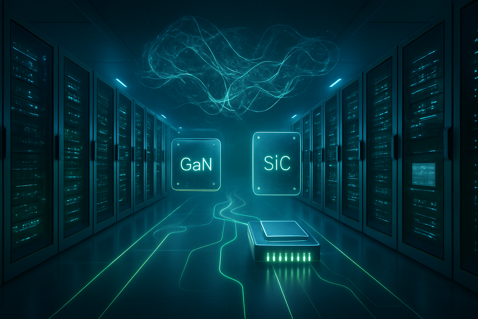
    Navitas Semiconductor's new product portfolio is a testament to the power of wide-bandgap materials in high-performance computing. The core of this innovation lies in two distinct categories of power devices tailored for different stages of Nvidia's 800 VDC power architecture:

    Firstly, 100V GaN FETs (Gallium Nitride Field-Effect Transistors) are specifically optimized for the critical lower-voltage DC-DC stages found directly on GPU power boards. In these highly localized environments, individual AI chips can draw over 1000W of power, demanding power conversion solutions that offer ultra-high density and exceptional thermal management. Navitas's GaN FETs excel here due to their superior switching speeds and lower on-resistance compared to traditional silicon-based MOSFETs, minimizing energy loss right at the point of consumption. This allows for more compact power delivery modules, enabling higher computational density within each AI server rack.

    Secondly, for the initial high-power conversion stages that handle the immense power flow from the utility grid to the 800V DC backbone of the AI data center, Navitas is deploying a combination of 650V GaN devices and high-voltage SiC (Silicon Carbide) devices. These components are instrumental in rectifying and stepping down the incoming AC power to the 800V DC rail with minimal losses. The higher voltage handling capabilities of SiC, coupled with the high-frequency switching and efficiency of GaN, allow for significantly more efficient power conversion across the entire data center infrastructure. This multi-material approach ensures optimal performance and efficiency at every stage of power delivery.

    This approach fundamentally differs from previous generations of AI data center power delivery, which typically relied on lower voltage (e.g., 54V) DC systems or multiple AC/DC and DC/DC conversion stages. The 800 VDC architecture, facilitated by Navitas's wide-bandgap components, streamlines power conversion by reducing the number of conversion steps, thereby maximizing energy efficiency, reducing resistive losses in cabling (which are proportional to the square of the current), and enhancing overall system reliability. For example, solutions leveraging these devices have achieved power supply units (PSUs) with up to 98% efficiency, with a 4.5 kW AI GPU power supply solution demonstrating an impressive power density of 137 W/in³. Initial reactions from the AI research community and industry experts have been overwhelmingly positive, highlighting the critical need for such advancements to sustain the rapid growth of AI and acknowledging Navitas's role in enabling this crucial infrastructure.

    Market Dynamics: Reshaping the AI Hardware Landscape

    The introduction of Navitas Semiconductor's advanced power solutions for Nvidia's 800 VDC AI architecture is set to profoundly impact various players across the AI and tech industries. Nvidia (NASDAQ: NVDA) stands to be a primary beneficiary, as these power semiconductors are integral to the success and widespread adoption of its next-generation AI infrastructure. By offering a more energy-efficient and high-performance power delivery system, Nvidia can further solidify its dominance in the AI accelerator market, making its "AI factories" more attractive to hyperscalers, cloud providers, and enterprises building massive AI models. The ability to manage power effectively is a key differentiator in a market where computational power and operational costs are paramount.

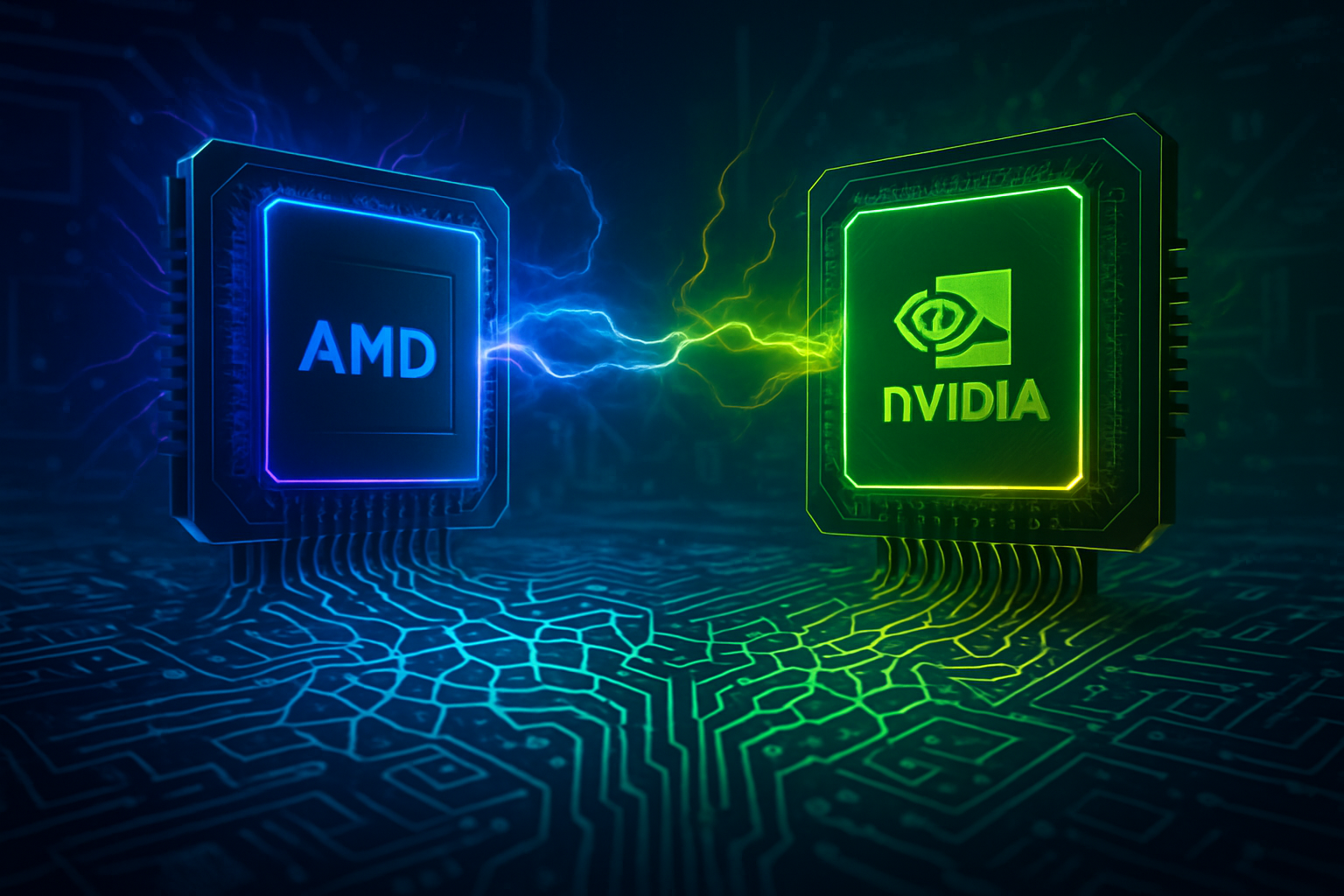
    Beyond Nvidia, other companies involved in the AI supply chain, particularly those manufacturing power supplies, server racks, and data center infrastructure, stand to benefit. Original Design Manufacturers (ODMs) and Original Equipment Manufacturers (OEMs) that integrate these power solutions into their server designs will gain a competitive edge by offering more efficient and dense AI computing platforms. This development could also spur innovation among cooling solution providers, as higher power densities necessitate more sophisticated thermal management. Conversely, companies heavily invested in traditional silicon-based power management solutions might face increased pressure to adapt or risk falling behind, as the efficiency gains offered by GaN and SiC become industry standards for AI.

    The competitive implications for major AI labs and tech companies are significant. As AI models become larger and more complex, the underlying infrastructure's efficiency directly translates to faster training times, lower operational costs, and greater scalability. Companies like Google (NASDAQ: GOOGL), Microsoft (NASDAQ: MSFT), Amazon (NASDAQ: AMZN), and Meta (NASDAQ: META), all of whom operate vast AI data centers, will likely prioritize adopting systems that leverage such advanced power delivery. This could disrupt existing product roadmaps for internal AI hardware development if their current power solutions cannot match the efficiency and density offered by Nvidia's 800V architecture enabled by Navitas. The strategic advantage lies with those who can deploy and scale AI infrastructure most efficiently, making power semiconductor innovation a critical battleground in the AI arms race.

    Broader Significance: A Cornerstone for Sustainable AI Growth

    Navitas's advancements in power semiconductors for Nvidia's 800V AI architecture fit perfectly into the broader AI landscape and current trends emphasizing sustainability and efficiency. As AI adoption accelerates globally, the energy footprint of AI data centers has become a significant concern. This development directly addresses that concern by offering a path to significantly reduce power consumption and associated carbon emissions. It aligns with the industry's push towards "green AI" and more environmentally responsible computing, a trend that is gaining increasing importance among investors, regulators, and the public.

    The impact extends beyond just energy savings. The ability to achieve higher power density means that more computational power can be packed into a smaller physical footprint, leading to more efficient use of real estate within data centers. This is crucial for "AI factories" that require multi-megawatt rack densities. Furthermore, simplified power conversion stages can enhance system reliability by reducing the number of components and potential points of failure, which is vital for continuous operation of mission-critical AI applications. Potential concerns, however, might include the initial cost of migrating to new 800V infrastructure and the supply chain readiness for wide-bandgap materials, although these are typically outweighed by the long-term operational benefits.

    Comparing this to previous AI milestones, this development can be seen as foundational, akin to breakthroughs in processor architecture or high-bandwidth memory. While not a direct AI algorithm innovation, it is an enabling technology that removes a significant bottleneck for AI's continued scaling. Just as faster GPUs or more efficient memory allowed for larger models, more efficient power delivery allows for more powerful and denser AI systems to operate sustainably. It represents a critical step in building the physical infrastructure necessary for the next generation of AI, from advanced generative models to real-time autonomous systems, ensuring that the industry can continue its rapid expansion without hitting power or thermal ceilings.

    The Road Ahead: Future Developments and Predictions

    The immediate future will likely see a rapid adoption of Navitas's GaN and SiC solutions within Nvidia's ecosystem, as AI data centers begin to deploy the 800V architecture. We can expect to see more detailed performance benchmarks and case studies emerging from early adopters, showcasing the real-world efficiency gains and operational benefits. In the near term, the focus will be on optimizing these power delivery systems further, potentially integrating more intelligent power management features and even higher power densities as wide-bandgap material technology continues to mature. The push for even higher voltages and more streamlined power conversion stages will persist.

    Looking further ahead, the potential applications and use cases are vast. Beyond hyperscale AI data centers, this technology could trickle down to enterprise AI deployments, edge AI computing, and even other high-power applications requiring extreme efficiency and density, such as electric vehicle charging infrastructure and industrial power systems. The principles of high-voltage DC distribution and wide-bandgap power conversion are universally applicable wherever significant power is consumed and efficiency is paramount. Experts predict that the move to 800V and beyond, facilitated by technologies like Navitas's, will become the industry standard for high-performance computing within the next five years, rendering older, less efficient power architectures obsolete.

    However, challenges remain. The scaling of wide-bandgap material production to meet potentially massive demand will be critical. Furthermore, ensuring interoperability and standardization across different vendors within the 800V ecosystem will be important for widespread adoption. As power densities increase, advanced cooling technologies, including liquid cooling, will become even more essential, creating a co-dependent innovation cycle. Experts also anticipate a continued convergence of power management and digital control, leading to "smarter" power delivery units that can dynamically optimize efficiency based on workload demands. The race for ultimate AI efficiency is far from over, and power semiconductors are at its heart.

    A New Era of AI Efficiency: Powering the Future

    In summary, Navitas Semiconductor's introduction of specialized GaN and SiC power devices for Nvidia's 800 VDC AI architecture marks a monumental step forward in the quest for more energy-efficient and high-performance artificial intelligence. The key takeaways are the significant improvements in power conversion efficiency (up to 98% for PSUs), the enhanced power density, and the fundamental shift towards a more streamlined, high-voltage DC distribution system in AI data centers. This innovation is not just about incremental gains; it's about laying the groundwork for the sustainable scalability of AI, addressing the critical bottleneck of power consumption that has loomed over the industry.

    This development's significance in AI history is profound, positioning it as an enabling technology that will underpin the next wave of AI breakthroughs. Without such advancements in power delivery, the exponential growth of AI models and the deployment of massive "AI factories" would be severely constrained by energy costs and thermal limits. Navitas, in collaboration with Nvidia, has effectively raised the ceiling for what is possible in AI computing infrastructure.

    In the coming weeks and months, industry watchers should keenly observe the adoption rates of Nvidia's 800V architecture and Navitas's integrated solutions. We should also watch for competitive responses from other power semiconductor manufacturers and infrastructure providers, as the race for AI efficiency intensifies. The long-term impact will be a greener, more powerful, and more scalable AI ecosystem, accelerating the development and deployment of advanced AI across every sector.


    This content is intended for informational purposes only and represents analysis of current AI developments.

    TokenRing AI delivers enterprise-grade solutions for multi-agent AI workflow orchestration, AI-powered development tools, and seamless remote collaboration platforms.
    For more information, visit https://www.tokenring.ai/.

  • The Silicon Backbone: How Semiconductor Innovation Fuels the AI Revolution

    The Silicon Backbone: How Semiconductor Innovation Fuels the AI Revolution

    The relentless march of artificial intelligence into every facet of technology and society is underpinned by a less visible, yet utterly critical, force: semiconductor innovation. These tiny chips, the foundational building blocks of all digital computation, are not merely components but the very accelerators of the AI revolution. As AI models grow exponentially in complexity and data demands, the pressure on semiconductor manufacturers to deliver faster, more efficient, and more specialized processing units intensifies, creating a symbiotic relationship where breakthroughs in one field directly propel the other.

    This dynamic interplay has never been more evident than in the current landscape, where the burgeoning demand for AI, particularly generative AI and large language models, is driving an unprecedented boom in the semiconductor market. Companies are pouring vast resources into developing next-generation chips tailored for AI workloads, optimizing for parallel processing, energy efficiency, and high-bandwidth memory. The immediate significance of this innovation is profound, leading to an acceleration of AI capabilities across industries, from scientific discovery and autonomous systems to healthcare and finance. Without the continuous evolution of semiconductor technology, the ambitious visions for AI would remain largely theoretical, highlighting the silicon backbone's indispensable role in transforming AI from a specialized technology into a foundational pillar of the global economy.

    Powering the Future: NVTS-Nvidia and the DGX Spark Initiative

    The intricate dance between semiconductor innovation and AI advancement is perfectly exemplified by strategic partnerships and pioneering hardware initiatives. A prime illustration of this synergy is the collaboration between Navitas Semiconductor (NVTS) (NASDAQ: NVTS) and Nvidia (NASDAQ: NVDA), alongside Nvidia's groundbreaking DGX Spark program. These developments underscore how specialized power delivery and integrated, high-performance computing platforms are pushing the boundaries of what AI can achieve.

    The NVTS-Nvidia collaboration, while not a direct chip fabrication deal in the traditional sense, highlights the critical role of power management in high-performance AI systems. Navitas Semiconductor specializes in gallium nitride (GaN) and silicon carbide (SiC) power semiconductors. These advanced materials offer significantly higher efficiency and power density compared to traditional silicon-based power electronics. For AI data centers, which consume enormous amounts of electricity, integrating GaN and SiC power solutions means less energy waste, reduced cooling requirements, and ultimately, more compact and powerful server designs. This allows for greater computational density within the same footprint, directly supporting the deployment of more powerful AI accelerators like Nvidia's GPUs. This differs from previous approaches that relied heavily on less efficient silicon power components, leading to larger power supplies, more heat, and higher operational costs. Initial reactions from the AI research community and industry experts emphasize the importance of such efficiency gains, noting that sustainable scaling of AI infrastructure is impossible without innovations in power delivery.

    Complementing this, Nvidia's DGX Spark program represents a significant leap in AI infrastructure. The DGX Spark is not a single product but an initiative to create fully integrated, enterprise-grade AI supercomputing solutions, often featuring Nvidia's most advanced GPUs (like the H100 or upcoming Blackwell series) interconnected with high-speed networking and sophisticated software stacks. The "Spark" aspect often refers to early access programs or specialized deployments designed to push the envelope of AI research and development. These systems are designed to handle the most demanding AI workloads, such as training colossal large language models (LLMs) with trillions of parameters or running complex scientific simulations. Technically, DGX systems integrate multiple GPUs, NVLink interconnects for ultra-fast GPU-to-GPU communication, and high-bandwidth memory, all optimized within a unified architecture. This integrated approach offers a stark contrast to assembling custom AI clusters from disparate components, providing a streamlined, high-performance, and scalable solution. Experts laud the DGX Spark initiative for democratizing access to supercomputing-level AI capabilities for enterprises and researchers, accelerating breakthroughs that would otherwise be hampered by infrastructure complexities.

    Reshaping the AI Landscape: Competitive Implications and Market Dynamics

    The innovations embodied by the NVTS-Nvidia synergy and the DGX Spark initiative are not merely technical feats; they are strategic maneuvers that profoundly reshape the competitive landscape for AI companies, tech giants, and startups alike. These advancements solidify the positions of certain players while simultaneously creating new opportunities and challenges across the industry.

    Nvidia (NASDAQ: NVDA) stands as the unequivocal primary beneficiary of these developments. Its dominance in the AI chip market is further entrenched by its ability to not only produce cutting-edge GPUs but also to build comprehensive, integrated AI platforms like the DGX series. By offering complete solutions that combine hardware, software (CUDA), and networking, Nvidia creates a powerful ecosystem that is difficult for competitors to penetrate. The DGX Spark program, in particular, strengthens Nvidia's ties with leading AI research institutions and enterprises, ensuring its hardware remains at the forefront of AI development. This strategic advantage allows Nvidia to dictate industry standards and capture a significant portion of the rapidly expanding AI infrastructure market.

    For other tech giants and AI labs, the implications are varied. Companies like Google (NASDAQ: GOOGL) and Amazon (NASDAQ: AMZN), which are heavily invested in their own custom AI accelerators (TPUs and Inferentia/Trainium, respectively), face continued pressure to match Nvidia's performance and ecosystem. While their internal chips offer optimization for their specific cloud services, Nvidia's broad market presence and continuous innovation force them to accelerate their own development cycles. Startups, on the other hand, often rely on readily available, powerful hardware to develop and deploy their AI solutions. The availability of highly optimized systems like DGX Spark, even through cloud providers, allows them to access supercomputing capabilities without the prohibitive cost and complexity of building their own from scratch, fostering innovation across the startup ecosystem. However, this also means many startups are inherently tied to Nvidia's ecosystem, creating a dependency that could have long-term implications for diversity in AI hardware.

    The potential disruption to existing products and services is significant. As AI capabilities become more powerful and accessible through optimized hardware, industries reliant on less sophisticated AI or traditional computing methods will need to adapt. For instance, enhanced generative AI capabilities powered by advanced semiconductors could disrupt content creation, drug discovery, and engineering design workflows. Companies that fail to leverage these new hardware capabilities to integrate cutting-edge AI into their offerings risk falling behind. Market positioning becomes crucial, with companies that can quickly adopt and integrate these new semiconductor-driven AI advancements gaining a strategic advantage. This creates a competitive imperative for continuous investment in AI infrastructure and talent, further intensifying the race to the top in the AI arms race.

    The Broader Canvas: AI's Trajectory and Societal Impacts

    The relentless evolution of semiconductor technology, epitomized by advancements like efficient power delivery for AI and integrated supercomputing platforms, paints a vivid picture of AI's broader trajectory. These developments are not isolated events but crucial milestones within the grand narrative of artificial intelligence, shaping its future and profoundly impacting society.

    These innovations fit squarely into the broader AI landscape's trend towards greater computational intensity and specialization. The ability to efficiently power and deploy massive AI models is directly enabling the continued scaling of large language models (LLMs), multimodal AI, and sophisticated autonomous systems. This pushes the boundaries of what AI can perceive, understand, and generate, moving us closer to truly intelligent machines. The focus on energy efficiency, driven by GaN and SiC power solutions, also aligns with a growing industry concern for sustainable AI, addressing the massive carbon footprint of training ever-larger models. Comparisons to previous AI milestones, such as the development of early neural networks or the ImageNet moment, reveal a consistent pattern: hardware breakthroughs have always been critical enablers of algorithmic advancements. Today's semiconductor innovations are fueling the "AI supercycle," accelerating progress at an unprecedented pace.

    The impacts are far-reaching. On the one hand, these advancements promise to unlock solutions to some of humanity's most pressing challenges, from accelerating drug discovery and climate modeling to revolutionizing education and accessibility. The enhanced capabilities of AI, powered by superior semiconductors, will drive unprecedented productivity gains and create entirely new industries and job categories. However, potential concerns also emerge. The immense computational power concentrated in a few hands raises questions about AI governance, ethical deployment, and the potential for misuse. The "AI divide" could widen, where nations or entities with access to cutting-edge semiconductor technology and AI expertise gain significant advantages over those without. Furthermore, the sheer energy consumption of AI, even with efficiency improvements, remains a significant environmental consideration, necessitating continuous innovation in both hardware and software optimization. The rapid pace of change also poses challenges for regulatory frameworks and societal adaptation, demanding proactive engagement from policymakers and ethicists.

    Glimpsing the Horizon: Future Developments and Expert Predictions

    Looking ahead, the symbiotic relationship between semiconductors and AI promises an even more dynamic and transformative future. Experts predict a continuous acceleration in both fields, with several key developments on the horizon.

    In the near term, we can expect continued advancements in specialized AI accelerators. Beyond current GPUs, the focus will intensify on custom ASICs (Application-Specific Integrated Circuits) designed for specific AI workloads, offering even greater efficiency and performance for tasks like inference at the edge. We will also see further integration of heterogeneous computing, where CPUs, GPUs, NPUs, and other specialized cores are seamlessly combined on a single chip or within a single system to optimize for diverse AI tasks. Memory innovation, particularly High Bandwidth Memory (HBM), will continue to evolve, with higher capacities and faster speeds becoming standard to feed the ever-hungry AI models. Long-term, the advent of novel computing paradigms like neuromorphic chips, which mimic the structure and function of the human brain for ultra-efficient processing, and potentially even quantum computing, could unlock AI capabilities far beyond what is currently imagined. Silicon photonics, using light instead of electrons for data transfer, is also on the horizon to address bandwidth bottlenecks.

    Potential applications and use cases are boundless. Enhanced AI, powered by these future semiconductors, will drive breakthroughs in personalized medicine, creating AI models that can analyze individual genomic data to tailor treatments. Autonomous systems, from self-driving cars to advanced robotics, will achieve unprecedented levels of perception and decision-making. Generative AI will become even more sophisticated, capable of creating entire virtual worlds, complex scientific simulations, and highly personalized educational content. Challenges, however, remain. The "memory wall" – the bottleneck between processing units and memory – will continue to be a significant hurdle. Power consumption, despite efficiency gains, will require ongoing innovation. The complexity of designing and manufacturing these advanced chips will also necessitate new AI-driven design tools and manufacturing processes. Experts predict that AI itself will play an increasingly critical role in designing the next generation of semiconductors, creating a virtuous cycle of innovation. The focus will also shift towards making AI more accessible and deployable at the edge, enabling intelligent devices to operate autonomously without constant cloud connectivity.

    The Unseen Engine: A Comprehensive Wrap-up of AI's Semiconductor Foundation

    The narrative of artificial intelligence in the 2020s is inextricably linked to the silent, yet powerful, revolution occurring within the semiconductor industry. The key takeaway from recent developments, such as the drive for efficient power solutions and integrated AI supercomputing platforms, is that hardware innovation is not merely supporting AI; it is actively defining its trajectory and potential. Without the continuous breakthroughs in chip design, materials science, and manufacturing processes, the ambitious visions for AI would remain largely theoretical.

    This development's significance in AI history cannot be overstated. We are witnessing a period where the foundational infrastructure for AI is being rapidly advanced, enabling the scaling of models and the deployment of capabilities that were unimaginable just a few years ago. The shift towards specialized accelerators, combined with a focus on energy efficiency, marks a mature phase in AI hardware development, moving beyond general-purpose computing to highly optimized solutions. This period will likely be remembered as the era when AI transitioned from a niche academic pursuit to a ubiquitous, transformative force, largely on the back of silicon's relentless progress.

    Looking ahead, the long-term impact of these advancements will be profound, shaping economies, societies, and even human capabilities. The continued democratization of powerful AI through accessible hardware will accelerate innovation across every sector. However, it also necessitates careful consideration of ethical implications, equitable access, and sustainable practices. What to watch for in the coming weeks and months includes further announcements of next-generation AI accelerators, strategic partnerships between chip manufacturers and AI developers, and the increasing adoption of AI-optimized hardware in cloud data centers and edge devices. The race for AI supremacy is, at its heart, a race for semiconductor superiority, and the finish line is nowhere in sight.


    This content is intended for informational purposes only and represents analysis of current AI developments.

    TokenRing AI delivers enterprise-grade solutions for multi-agent AI workflow orchestration, AI-powered development tools, and seamless remote collaboration platforms.
    For more information, visit https://www.tokenring.ai/.

  • Nvidia Unleashes DGX Spark: The World’s Smallest AI Supercomputer Ignites a New Era of Local AI

    Nvidia Unleashes DGX Spark: The World’s Smallest AI Supercomputer Ignites a New Era of Local AI

    REDMOND, WA – October 14, 2025 – In a move set to redefine the landscape of artificial intelligence development, Nvidia (NASDAQ: NVDA) has officially begun shipping its groundbreaking DGX Spark. Marketed as the "world's smallest AI supercomputer," this compact yet immensely powerful device, first announced in March 2025, is now making its way to developers and researchers, promising to democratize access to high-performance AI computing. The DGX Spark aims to bring data center-grade capabilities directly to the desktop, empowering individuals and small teams to tackle complex AI models previously confined to expansive cloud infrastructures or large-scale data centers.

    This launch marks a pivotal moment, as Nvidia continues its aggressive push to innovate across the AI hardware spectrum. By condensing petaFLOP-scale performance into a device roughly the size of a hardcover book, the DGX Spark is poised to accelerate the pace of AI innovation, enabling faster prototyping, local fine-tuning of large language models (LLMs), and enhanced privacy for sensitive AI workloads. Its arrival is anticipated to spark a new wave of creativity and efficiency among AI practitioners worldwide, fostering an environment where advanced AI development is no longer limited by physical space or prohibitive infrastructure costs.

    A Technical Marvel: Shrinking the Supercomputer

    The Nvidia DGX Spark is an engineering marvel, leveraging the cutting-edge NVIDIA GB10 Grace Blackwell Superchip architecture to deliver unprecedented power in a desktop form factor. At its core, the system boasts up to 1 petaFLOP of AI performance at FP4 precision with sparsity, a figure that rivals many full-sized data center servers from just a few years ago. This formidable processing power is complemented by a substantial 128 GB of LPDDR5x coherent unified system memory, a critical feature that allows the DGX Spark to effortlessly handle AI development and testing workloads with models up to 200 billion parameters. Crucially, this unified memory architecture enables fine-tuning of models up to 70 billion parameters locally without the typical quantization compromises often required on less capable hardware.

    Under the hood, the DGX Spark integrates a robust 20-core Arm CPU, featuring a combination of 10 Cortex-X925 performance cores and 10 Cortex-A725 efficiency cores, ensuring a balanced approach to compute-intensive tasks and general system operations. Storage is ample, with 4 TB of NVMe M.2 storage, complete with self-encryption for enhanced security. The system runs on NVIDIA DGX OS, a specialized version of Ubuntu, alongside Nvidia's comprehensive AI software stack, including essential CUDA libraries. For networking, it features NVIDIA ConnectX-7 Smart NIC, offering two QSFP ports with up to 200 Gbps, enabling developers to link two DGX Spark systems to work with even larger AI models, up to 405 billion parameters. This level of performance and memory in a device measuring just 150 x 150 x 50.5 mm and weighing 1.2 kg is a significant departure from previous approaches, which typically required rack-mounted servers or multi-GPU workstations, distinguishing it sharply from existing consumer-grade GPUs that often hit VRAM limitations with large models. Initial reactions from the AI research community have been overwhelmingly positive, highlighting the potential for increased experimentation and reduced dependency on costly cloud GPU instances.

    Reshaping the AI Industry: Beneficiaries and Battlefield

    The introduction of the Nvidia DGX Spark is poised to send ripples throughout the AI industry, creating new opportunities and intensifying competition. Startups and independent AI researchers stand to benefit immensely, as the DGX Spark provides an accessible entry point into serious AI development without the prohibitive upfront costs or ongoing operational expenses associated with cloud-based supercomputing. This could foster a new wave of innovation from smaller entities, allowing them to prototype, train, and fine-tune advanced models more rapidly and privately. Enterprises dealing with sensitive data, such as those in healthcare, finance, or defense, could leverage the DGX Spark for on-premise AI development, mitigating data privacy and security concerns inherent in cloud environments.

    For major AI labs and tech giants, the DGX Spark could serve as a powerful edge device for distributed AI training, local model deployment, and specialized research tasks. It may also influence their strategies for hybrid cloud deployments, enabling more workloads to be processed locally before scaling to larger cloud clusters. The competitive implications are significant; while cloud providers like Amazon (NASDAQ: AMZN) Web Services, Microsoft (NASDAQ: MSFT) Azure, and Google (NASDAQ: GOOGL) Cloud still offer unparalleled scalability, the DGX Spark presents a compelling alternative for specific use cases, potentially slowing the growth of certain cloud-based AI development segments. This could lead to a shift in how AI infrastructure is consumed, with a greater emphasis on local, powerful devices for initial development and experimentation. The $3,999.99 price point makes it an attractive proposition, positioning Nvidia to capture a segment of the market that seeks high-performance AI compute without the traditional data center footprint.

    Wider Significance: Democratizing AI and Addressing Challenges

    The DGX Spark's arrival fits squarely into the broader trend of democratizing AI, making advanced capabilities accessible to a wider audience. It represents a significant step towards enabling "AI at the edge" for development purposes, allowing sophisticated models to be built and refined closer to the data source. This has profound impacts on various sectors, from accelerating scientific discovery in academia to enabling more agile product development in commercial industries. The ability to run large models locally can reduce latency, improve data privacy, and potentially lower overall operational costs for many organizations.

    However, its introduction also raises potential concerns. While the initial price is competitive for its capabilities, it still represents a significant investment for individual developers or very small teams. The power consumption, though efficient for its performance, is still 240 watts, which might be a consideration for continuous, always-on operations in a home office setting. Compared to previous AI milestones, such as the introduction of CUDA-enabled GPUs or the first DGX systems, the DGX Spark signifies a miniaturization and decentralization of supercomputing power, pushing the boundaries of what's possible on a desktop. It moves beyond merely accelerating inference to enabling substantial local training and fine-tuning, a critical step for personalized and specialized AI applications.

    The Road Ahead: Applications and Expert Predictions

    Looking ahead, the DGX Spark is expected to catalyze a surge in innovative applications. Near-term developments will likely see its adoption by individual researchers and small development teams for rapid prototyping of generative AI models, drug discovery simulations, and advanced robotics control algorithms. In the long term, its capabilities could enable hyper-personalized AI experiences on local devices, supporting scenarios like on-device large language model inference for privacy-sensitive applications, or advanced computer vision systems that perform real-time analysis without cloud dependency. It could also become a staple in educational institutions, providing students with hands-on experience with supercomputing-level AI.

    However, challenges remain. The ecosystem of software tools and optimized models for such a compact yet powerful device will need to mature further. Ensuring seamless integration with existing AI workflows and providing robust support will be crucial for widespread adoption. Experts predict that the DGX Spark will accelerate the development of specialized, domain-specific AI models, as developers can iterate faster and more privately. It could also spur further miniaturization efforts from competitors, leading to an arms race in compact, high-performance AI hardware. The ability to run large models locally will also push the boundaries of what's considered "edge computing," blurring the lines between traditional data centers and personal workstations.

    A New Dawn for AI Development

    Nvidia's DGX Spark is more than just a new piece of hardware; it's a testament to the relentless pursuit of making advanced AI accessible and efficient. The key takeaway is the unprecedented convergence of supercomputing power, substantial unified memory, and a compact form factor, all at a price point that broadens its appeal significantly. This development's significance in AI history cannot be overstated, as it marks a clear shift towards empowering individual practitioners and smaller organizations with the tools necessary to innovate at the forefront of AI. It challenges the traditional reliance on massive cloud infrastructure for certain types of AI development, offering a powerful, local alternative.

    In the coming weeks and months, the tech world will be closely watching the initial adoption rates and the innovative projects that emerge from DGX Spark users. Its impact on fields requiring high data privacy, rapid iteration, and localized processing will be particularly telling. As AI continues its exponential growth, devices like the DGX Spark will play a crucial role in shaping its future, fostering a more distributed, diverse, and dynamic ecosystem of AI development.


    This content is intended for informational purposes only and represents analysis of current AI developments.

    TokenRing AI delivers enterprise-grade solutions for multi-agent AI workflow orchestration, AI-powered development tools, and seamless remote collaboration platforms.
    For more information, visit https://www.tokenring.ai/.

  • Navitas Semiconductor (NVTS) Soars on Landmark Deal to Power Nvidia’s 800 VDC AI Factories

    Navitas Semiconductor (NVTS) Soars on Landmark Deal to Power Nvidia’s 800 VDC AI Factories

    SAN JOSE, CA – October 14, 2025 – Navitas Semiconductor (NASDAQ: NVTS) witnessed an unprecedented surge in its stock value yesterday, climbing over 27% in a single day, following the announcement of significant progress in its partnership with AI giant Nvidia (NASDAQ: NVDA). The deal positions Navitas as a critical enabler for Nvidia's next-generation 800 VDC AI architecture systems, a development set to revolutionize power delivery in the rapidly expanding "AI factory" era. This collaboration not only validates Navitas's advanced Gallium Nitride (GaN) and Silicon Carbide (SiC) power semiconductor technologies but also signals a fundamental shift in how the industry will power the insatiable demands of future AI workloads.

    The strategic alliance underscores a pivotal moment for both companies. For Navitas, it signifies a major expansion beyond its traditional consumer fast charger market, cementing its role in high-growth, high-performance computing. For Nvidia, it secures a crucial component in its quest to build the most efficient and powerful AI infrastructure, ensuring its cutting-edge GPUs can operate at peak performance within demanding multi-megawatt data centers. The market's enthusiastic reaction reflects the profound implications this partnership holds for the efficiency, scalability, and sustainability of the global AI chip ecosystem.

    Engineering the Future of AI Power: Navitas's Role in Nvidia's 800 VDC Architecture

    The technical cornerstone of this partnership lies in Navitas Semiconductor's (NASDAQ: NVTS) advanced wide-bandgap (WBG) power semiconductors, specifically tailored to meet the rigorous demands of Nvidia's (NASDAQ: NVDA) groundbreaking 800 VDC AI architecture. Announced on October 13, 2025, this development builds upon Navitas's earlier disclosure on May 21, 2025, regarding its commitment to supporting Nvidia's Kyber rack-scale systems. The transition to 800 VDC is not merely an incremental upgrade but a transformative leap designed to overcome the limitations of legacy 54V architectures, which are increasingly inadequate for the multi-megawatt rack densities of modern AI factories.

    Navitas is leveraging its expertise in both GaNFast™ gallium nitride and GeneSiC™ silicon carbide technologies. For the critical lower-voltage DC-DC stages on GPU power boards, Navitas has introduced a new portfolio of 100 V GaN FETs. These components are engineered for ultra-high density and precise thermal management, crucial for the compact and power-intensive environments of next-generation AI compute platforms. These GaN FETs are fabricated using a 200mm GaN-on-Si process, a testament to Navitas's manufacturing prowess. Complementing these, Navitas is also providing 650V GaN and high-voltage SiC devices, which manage various power conversion stages throughout the data center, from the utility grid all the way to the GPU. The company's GeneSiC technology, boasting over two decades of innovation, offers robust voltage ranges from 650V to an impressive 6,500V.

    What sets Navitas's approach apart is its integration of advanced features like GaNSafe™ power ICs, which incorporate control, drive, sensing, and critical protection mechanisms to ensure unparalleled reliability and robustness. Furthermore, the innovative "IntelliWeave™" digital control technique, when combined with high-power GaNSafe and Gen 3-Fast SiC MOSFETs, enables power factor correction (PFC) peak efficiencies of up to 99.3%, slashing power losses by 30% compared to existing solutions. This level of efficiency is paramount for AI data centers, where every percentage point of power saved translates into significant operational cost reductions and environmental benefits. The 800 VDC architecture itself allows for direct conversion from 13.8 kVAC utility power, streamlining the power train, reducing resistive losses, and potentially improving end-to-end efficiency by up to 5% over current 54V systems, while also significantly reducing copper usage by up to 45% for a 1MW rack.

    Reshaping the AI Chip Market: Competitive Implications and Strategic Advantages

    This landmark partnership between Navitas Semiconductor (NASDAQ: NVTS) and Nvidia (NASDAQ: NVDA) is poised to send ripples across the AI chip market, redefining competitive landscapes and solidifying strategic advantages for both companies. For Navitas, the deal represents a profound validation of its wide-bandgap (GaN and SiC) technologies, catapulting it into the lucrative and rapidly expanding AI data center infrastructure market. The immediate stock surge, with NVTS shares climbing over 21% on October 13 and extending gains by an additional 30% in after-hours trading, underscores the market's recognition of this strategic pivot. Navitas is now repositioning its business strategy to focus heavily on AI data centers, targeting a substantial $2.6 billion market by 2030, a significant departure from its historical focus on consumer electronics.

    For Nvidia, the collaboration is equally critical. As the undisputed leader in AI GPUs, Nvidia's ability to maintain its edge hinges on continuous innovation in performance and, crucially, power efficiency. Navitas's advanced GaN and SiC solutions are indispensable for Nvidia to achieve the unprecedented power demands and optimal efficiency required for its next-generation AI computing platforms, such such as the NVIDIA Rubin Ultra and Kyber rack architecture. By partnering with Navitas, Nvidia ensures it has access to the most advanced power delivery solutions, enabling its GPUs to operate at peak performance within its demanding "AI factories." This strategic move helps Nvidia drive the transformation in AI infrastructure, maintaining its competitive lead against rivals like AMD (NASDAQ: AMD) and Intel (NASDAQ: INTC) in the high-stakes AI accelerator market.

    The implications extend beyond the immediate partners. This architectural shift to 800 VDC, spearheaded by Nvidia and enabled by Navitas, will likely compel other power semiconductor providers to accelerate their own wide-bandgap technology development. Companies reliant on traditional silicon-based power solutions may find themselves at a competitive disadvantage as the industry moves towards higher efficiency and density. This development also highlights the increasing interdependency between AI chip designers and specialized power component manufacturers, suggesting that similar strategic partnerships may become more common as AI systems continue to push the boundaries of power consumption and thermal management. Furthermore, the reduced copper usage and improved efficiency offered by 800 VDC could lead to significant cost savings for hyperscale data center operators and cloud providers, potentially influencing their choice of AI infrastructure.

    A New Dawn for Data Centers: Wider Significance in the AI Landscape

    The collaboration between Navitas Semiconductor (NASDAQ: NVTS) and Nvidia (NASDAQ: NVDA) to drive the 800 VDC AI architecture is more than just a business deal; it signifies a fundamental paradigm shift within the broader AI landscape and data center infrastructure. This move directly addresses one of the most pressing challenges facing the "AI factory" era: the escalating power demands of AI workloads. As AI compute platforms push rack densities beyond 300 kilowatts, with projections of exceeding 1 megawatt per rack in the near future, traditional 54V power distribution systems are simply unsustainable. The 800 VDC architecture represents a "transformational rather than evolutionary" step, as articulated by Navitas's CEO, marking a critical milestone in the pursuit of scalable and sustainable AI.

    This development fits squarely into the overarching trend of optimizing every layer of the AI stack for efficiency and performance. While much attention is often paid to the AI chips themselves, the power delivery infrastructure is an equally critical, yet often overlooked, component. Inefficient power conversion not only wastes energy but also generates significant heat, adding to cooling costs and limiting overall system density. By adopting 800 VDC, the industry is moving towards a streamlined power train that reduces resistive losses and maximizes energy efficiency by up to 5% compared to current 54V systems. This has profound impacts on the total cost of ownership for AI data centers, making large-scale AI deployments more economically viable and environmentally responsible.

    Potential concerns, however, include the significant investment required for data centers to transition to this new architecture. While the long-term benefits are clear, the initial overhaul of existing infrastructure could be a hurdle for some operators. Nevertheless, the benefits of improved reliability, reduced copper usage (up to 45% for a 1MW rack), and maximized white space for revenue-generating compute are compelling. This architectural shift can be compared to previous AI milestones such as the widespread adoption of GPUs for general-purpose computing, or the development of specialized AI accelerators. Just as those advancements enabled new levels of computational power, the 800 VDC architecture will enable unprecedented levels of power density and efficiency, unlocking the next generation of AI capabilities. It underscores that innovation in AI is not solely about algorithms or chip design, but also about the foundational infrastructure that powers them.

    The Road Ahead: Future Developments and AI's Power Frontier

    The groundbreaking partnership between Navitas Semiconductor (NASDAQ: NVTS) and Nvidia (NASDAQ: NVDA) heralds a new era for AI infrastructure, with significant developments expected on the horizon. The transition to the 800 VDC architecture, which Nvidia (NASDAQ: NVDA) is leading and anticipates commencing in 2027, will be a gradual but impactful shift across the data center electrical ecosystem. Near-term developments will likely focus on the widespread adoption and integration of Navitas's GaN and SiC power devices into Nvidia's AI factory computing platforms, including the NVIDIA Rubin Ultra. This will involve rigorous testing and optimization to ensure seamless operation and maximal efficiency in real-world, high-density AI environments.

    Looking further ahead, the potential applications and use cases are vast. The ability to efficiently power multi-megawatt IT racks will unlock new possibilities for hyperscale AI model training, complex scientific simulations, and the deployment of increasingly sophisticated AI services. We can expect to see data centers designed from the ground up to leverage 800 VDC, enabling unprecedented computational density and reducing the physical footprint required for massive AI operations. This could lead to more localized AI factories, closer to data sources, or more compact, powerful edge AI deployments. Experts predict that this fundamental architectural change will become the industry standard for high-performance AI computing, pushing traditional 54V systems into obsolescence for demanding AI workloads.

    However, challenges remain. The industry will need to address standardization across various components of the 800 VDC ecosystem, ensuring interoperability and ease of deployment. Supply chain robustness for wide-bandgap semiconductors will also be crucial, as demand for GaN and SiC devices is expected to skyrocket. Furthermore, the thermal management of these ultra-dense racks, even with improved power efficiency, will continue to be a significant engineering challenge, requiring innovative cooling solutions. What experts predict will happen next is a rapid acceleration in the development and deployment of 800 VDC compatible power supplies, server racks, and related infrastructure, with a strong focus on maximizing every watt of power to fuel the next wave of AI innovation.

    Powering the Future: A Comprehensive Wrap-Up of AI's New Energy Backbone

    The stock surge experienced by Navitas Semiconductor (NASDAQ: NVTS) following its deal to supply power semiconductors for Nvidia's (NASDAQ: NVDA) 800 VDC AI architecture system marks a pivotal moment in the evolution of artificial intelligence infrastructure. The key takeaway is the undeniable shift towards higher voltage, more efficient power delivery systems, driven by the insatiable power demands of modern AI. Navitas's advanced GaN and SiC technologies are not just components; they are the essential backbone enabling Nvidia's vision of ultra-efficient, multi-megawatt AI factories. This partnership validates Navitas's strategic pivot into the high-growth AI data center market and secures Nvidia's leadership in providing the most powerful and efficient AI computing platforms.

    This development's significance in AI history cannot be overstated. It represents a fundamental architectural change in how AI data centers will be designed and operated, moving beyond the limitations of legacy power systems. By significantly improving power efficiency, reducing resistive losses, and enabling unprecedented power densities, the 800 VDC architecture will directly facilitate the training of larger, more complex AI models and the deployment of more sophisticated AI services. It highlights that innovation in AI is not confined to algorithms or processors but extends to every layer of the technology stack, particularly the often-underestimated power delivery system. This move will have lasting impacts on operational costs, environmental sustainability, and the sheer computational scale achievable for AI.

    In the coming weeks and months, industry observers should watch for further announcements regarding the adoption of 800 VDC by other major players in the data center and AI ecosystem. Pay close attention to Navitas's continued expansion into the AI market and its financial performance as it solidifies its position as a critical power semiconductor provider. Similarly, monitor Nvidia's progress in deploying its 800 VDC-enabled AI factories and how this translates into enhanced performance and efficiency for its AI customers. This partnership is a clear indicator that the race for AI dominance is now as much about efficient power as it is about raw processing power.


    This content is intended for informational purposes only and represents analysis of current AI developments.

    TokenRing AI delivers enterprise-grade solutions for multi-agent AI workflow orchestration, AI-powered development tools, and seamless remote collaboration platforms.
    For more information, visit https://www.tokenring.ai/.

  • TSMC’s Q3 2025 Earnings Propel AI Revolution Amid Bullish Outlook

    TSMC’s Q3 2025 Earnings Propel AI Revolution Amid Bullish Outlook

    Taipei, Taiwan – October 14, 2025 – Taiwan Semiconductor Manufacturing Company (NYSE: TSM), the undisputed titan of the semiconductor foundry industry, is poised to announce a blockbuster third quarter for 2025. Widespread anticipation and a profoundly bullish outlook are sweeping through the tech world, driven by the insatiable global demand for artificial intelligence (AI) chips. Analysts are projecting record-breaking revenue and net profit figures, cementing TSMC's indispensable role as the "unseen architect" of the AI supercycle and signaling a robust health for the broader tech ecosystem.

    The immediate significance of TSMC's anticipated Q3 performance cannot be overstated. As the primary manufacturer of the most advanced processors for leading AI companies, TSMC's financial health serves as a critical barometer for the entire AI and high-performance computing (HPC) landscape. A strong report will not only validate the ongoing AI supercycle but also reinforce TSMC's market leadership and its pivotal role in enabling the next generation of technological innovation.

    Analyst Expectations Soar Amidst AI-Driven Demand and Strategic Pricing

    The financial community is buzzing with optimism for TSMC's Q3 2025 earnings, with specific forecasts painting a picture of exceptional growth. Analysts widely anticipated TSMC's Q3 2025 revenue to fall between $31.8 billion and $33 billion, representing an approximate 38% year-over-year increase at the midpoint. Preliminary sales data confirmed a strong performance, with Q3 revenue reaching NT$989.918 billion ($32.3 billion), exceeding most analyst expectations. This robust growth is largely attributed to the relentless demand for AI accelerators and high-end computing components.

    Net profit projections are equally impressive. A consensus among analysts, including an LSEG SmartEstimate compiled from 20 analysts, forecast a net profit of NT$415.4 billion ($13.55 billion) for the quarter. This would mark a staggering 28% increase from the previous year, setting a new record for the company's highest quarterly profit in its history and extending its streak to a seventh consecutive quarter of profit growth. Wall Street analysts generally expected earnings per share (EPS) of $2.63, reflecting a 35% year-over-year increase, with the Zacks Consensus Estimate adjusted upwards to $2.59 per share, indicating a 33.5% year-over-year growth.

    A key driver of this financial strength is TSMC's improving pricing power for its advanced nodes. Reports indicate that TSMC plans for a 5% to 10% price hike for advanced node processes in 2025. This increase is primarily a response to rising production costs, particularly at its new Arizona facility, where manufacturing expenses are estimated to be at least 30% higher than in Taiwan. However, tight production capacity for cutting-edge technologies also contributes to this upward price pressure. Major clients such as Apple (NASDAQ: AAPL), Advanced Micro Devices (NASDAQ: AMD), and Nvidia (NASDAQ: NVDA), who are heavily reliant on these advanced nodes, are expected to absorb these higher manufacturing costs, demonstrating TSMC's indispensable position. For instance, TSMC has set the price for its upcoming 2nm wafers at approximately $30,000 each, a 15-20% increase over the average $25,000-$27,000 price for its 3nm process.

    TSMC's technological leadership and dominance in advanced semiconductor manufacturing processes are crucial to its Q3 success. Its strong position in 3-nanometer (3nm) and 5-nanometer (5nm) manufacturing nodes is central to the revenue surge, with these advanced nodes collectively representing 74% of total wafer revenue in Q2 2025. Production ramp-up of 3nm chips, vital for AI and HPC devices, is progressing faster than anticipated, with 3nm lines operating at full capacity. The "insatiable demand" for AI chips, particularly from companies like Nvidia, Apple, AMD, and Broadcom (NASDAQ: AVGO), continues to be the foremost driver, fueling substantial investments in AI infrastructure and cloud computing.

    TSMC's Indispensable Role: Reshaping the AI and Tech Landscape

    TSMC's strong Q3 2025 performance and bullish outlook are poised to profoundly impact the artificial intelligence and broader tech industry, solidifying its role as the foundational enabler of the AI supercycle. The company's unique manufacturing capabilities mean that its success directly translates into opportunities and challenges across the industry.

    Major beneficiaries of TSMC's technological prowess include the leading players in AI and high-performance computing. Nvidia, for example, is heavily dependent on TSMC for its cutting-edge GPUs, such as the H100 and upcoming architectures like Blackwell and Rubin, with TSMC's advanced CoWoS (Chip-on-Wafer-on-Substrate) packaging technology being indispensable for integrating high-bandwidth memory. Apple relies on TSMC's 3nm process for its M4 and M5 chips, powering on-device AI capabilities. Advanced Micro Devices (NASDAQ: AMD) utilizes TSMC's advanced packaging and leading-edge nodes for its next-generation data center GPUs and EPYC CPUs, positioning itself as a strong contender in the HPC market. Hyperscalers like Alphabet (NASDAQ: GOOGL), Amazon (NASDAQ: AMZN), Meta Platforms (NASDAQ: META), and Microsoft (NASDAQ: MSFT) are increasingly designing their own custom AI silicon (ASICs) and are significant customers for TSMC's advanced nodes, including the upcoming 2nm process.

    The competitive implications for major AI labs and tech companies are significant. TSMC's indispensable position centralizes the AI hardware ecosystem around a select few dominant players who can secure access to its advanced manufacturing capabilities. This creates substantial barriers to entry for newer firms or those without significant capital or strategic partnerships. While Intel (NASDAQ: INTC) is working to establish its own competitive foundry business, TSMC's advanced-node manufacturing capabilities are widely recognized as superior, creating a significant gap. The continuous push for more powerful and energy-efficient AI chips directly disrupts existing products and services that rely on older, less efficient hardware. Companies unable to upgrade their AI infrastructure or adapt to the rapid advancements risk falling behind in performance, cost-efficiency, and capabilities.

    In terms of market positioning, TSMC maintains its undisputed position as the world's leading pure-play semiconductor foundry, holding over 70.2% of the global pure-play foundry market and an even higher share in advanced AI chip production. Its technological prowess, mastering cutting-edge process nodes (3nm, 2nm, A16, A14 for 2028) and innovative packaging solutions (CoWoS, SoIC), provides an unparalleled strategic advantage. The 2nm (N2) process, featuring Gate-All-Around (GAA) nanosheet transistors, is on track for mass production in the second half of 2025, with demand already exceeding initial capacity. Furthermore, TSMC is pursuing a "System Fab" strategy, offering a comprehensive suite of interconnected technologies, including advanced 3D chip stacking and packaging (TSMC 3DFabric®) to enable greater performance and power efficiency for its customers.

    Wider Significance: AI Supercycle Validation and Geopolitical Crossroads

    TSMC's exceptional Q3 2025 performance is more than just a corporate success story; it is a profound validation of the ongoing AI supercycle and a testament to the transformative power of advanced semiconductor technology. The company's financial health is a direct reflection of the global AI chip market's explosive growth, projected to increase from an estimated $123.16 billion in 2024 to $311.58 billion by 2029, with AI chips contributing over $150 billion to total semiconductor sales in 2025 alone.

    This success highlights several key trends in the broader AI landscape. Hardware has re-emerged as a strategic differentiator, with custom AI chips (NPUs, TPUs, specialized AI accelerators) becoming ubiquitous. TSMC's dominance in advanced nodes and packaging is crucial for the parallel processing, high data transfer speeds, and energy efficiency required by modern AI accelerators and large language models. There's also a significant shift towards edge AI and energy efficiency, as AI deployments scale and demand low-power, high-efficiency chips for applications from autonomous vehicles to smart cameras.

    The broader impacts are substantial. TSMC's growth acts as a powerful economic catalyst, driving innovation and investment across the entire tech ecosystem. Its capabilities accelerate the iteration of chip technology, compelling companies to continuously upgrade their AI infrastructure. This profoundly reshapes the competitive landscape for AI companies, creating clear beneficiaries among major tech giants that rely on TSMC for their most critical AI and high-performance chips.

    However, TSMC's centrality to the AI landscape also highlights significant vulnerabilities and concerns. The "extreme supply chain concentration" in Taiwan, where over 90% of the world's most advanced chips are manufactured by TSMC and Samsung (KRX: 005930), creates a critical single point of failure. Escalating geopolitical tensions in the Taiwan Strait pose a severe risk, with potential military conflict or economic blockade capable of crippling global AI infrastructure. TSMC is actively trying to mitigate this by diversifying its manufacturing footprint with significant investments in the U.S. (Arizona), Japan, and Germany. The U.S. CHIPS Act is also a strategic initiative to secure domestic semiconductor production and reduce reliance on foreign manufacturing. Beyond Taiwan, the broader AI chip supply chain relies on a concentrated "triumvirate" of Nvidia (chip designs), ASML (AMS: ASML) (precision lithography equipment), and TSMC (manufacturing), creating further single points of failure.

    Comparing this to previous AI milestones, the current growth phase, heavily reliant on TSMC's manufacturing prowess, represents a unique inflection point. Unlike previous eras where hardware was more of a commodity, the current environment positions advanced hardware as a "strategic differentiator." This "sea change" in generative AI is being compared to fundamental technology shifts like the internet, mobile, and cloud computing, indicating a foundational transformation across industries.

    Future Horizons: Unveiling Next-Generation AI and Global Expansion

    Looking ahead, TSMC's future developments are characterized by an aggressive technology roadmap, continued advancements in manufacturing and packaging, and strategic global diversification, all geared towards sustaining its leadership in the AI era.

    In the near term, TSMC's 3nm (N3 family) process, already in volume production, will remain a workhorse for current high-performance AI chips. However, the true game-changer will be the mass production of the 2nm (N2) process node, ramping up in late 2025. Major clients like Apple, Advanced Micro Devices (NASDAQ: AMD), Intel (NASDAQ: INTC), Nvidia (NASDAQ: NVDA), Qualcomm (NASDAQ: QCOM), and MediaTek are expected to utilize this node, which promises a 25-30% reduction in power consumption or a 10-15% increase in performance compared to 3nm chips. TSMC projects initial 2nm capacity to reach over 100,000 wafers per month in 2026. Beyond 2nm, the A16 (1.6nm-class) technology is slated for production readiness in late 2026, followed by A14 (1.4nm-class) for mass production in the second half of 2028, further pushing the boundaries of chip density and efficiency.

    Advanced packaging technologies are equally critical. TSMC is aggressively expanding its CoWoS (Chip-on-Wafer-on-Substrate) advanced packaging capacity, aiming to quadruple its output by the end of 2025 and further increase it to 130,000 wafers per month by 2026 to meet surging AI demand. Innovations like CoWoS-L (expected 2027) and SoIC (System-on-Integrated-Chips) will enable even denser chip stacking and integration, crucial for the complex architectures of future AI accelerators.

    The ongoing advancements in AI chips are enabling a vast array of new and enhanced applications. Beyond data centers and cloud computing, there is a significant shift towards deploying AI at the edge, including autonomous vehicles, industrial robotics, smart cameras, mobile devices, and various IoT devices, demanding low-power, high-efficiency chips like Neural Processing Units (NPUs). AI-enabled PCs are expected to constitute 43% of all shipments by the end of 2025. In healthcare, AI chips are crucial for medical imaging systems with superhuman accuracy and powering advanced computations in scientific research and drug discovery.

    Despite the rapid progress, several significant challenges need to be overcome. Manufacturing complexity and cost remain immense, with a new fabrication plant costing $15B-$20B. Design and packaging hurdles, such as optimizing performance while reducing immense power consumption and managing heat dissipation, are critical. Supply chain and geopolitical risks, particularly the concentration of advanced manufacturing in Taiwan, continue to be a major concern, driving TSMC's strategic global expansion into the U.S. (Arizona), Japan, and Germany. The immense energy consumption of AI infrastructure also raises significant environmental concerns, making energy efficiency a crucial area for innovation.

    Industry experts are highly optimistic, predicting TSMC will remain the "indispensable architect of the AI supercycle," with its market dominance and growth trajectory defining the future of AI hardware. The global AI chip market is projected to skyrocket to an astonishing $311.58 billion by 2029, or around $295.56 billion by 2030, with a Compound Annual Growth Rate (CAGR) of 33.2% from 2025 to 2030. The intertwining of AI and semiconductors is projected to contribute more than $15 trillion to the global economy by 2030.

    A New Era: TSMC's Enduring Legacy and the Road Ahead

    TSMC's anticipated Q3 2025 earnings mark a pivotal moment, not just for the company, but for the entire technological landscape. The key takeaway is clear: TSMC's unparalleled leadership in advanced semiconductor manufacturing is the bedrock upon which the current AI revolution is being built. The strong revenue growth, robust net profit projections, and improving pricing power are all direct consequences of the "insatiable demand" for AI chips and the company's continuous innovation in process technology and advanced packaging.

    This development holds immense significance in AI history, solidifying TSMC's role as the "unseen architect" that enables breakthroughs across every facet of artificial intelligence. Its pure-play foundry model has fostered an ecosystem where innovation in chip design can flourish, driving the rapid advancements seen in AI models today. The long-term impact on the tech industry is profound, centralizing the AI hardware ecosystem around TSMC's capabilities, accelerating hardware obsolescence, and dictating the pace of technological progress. However, it also highlights the critical vulnerabilities associated with supply chain concentration, especially amidst escalating geopolitical tensions.

    In the coming weeks and months, all eyes will be on TSMC's official Q3 2025 earnings report and the subsequent earnings call on October 16, 2025. Investors will be keenly watching for any upward revisions to full-year 2025 revenue forecasts and crucial fourth-quarter guidance. Geopolitical developments, particularly concerning US tariffs and trade relations, remain a critical watch point, as proposed tariffs or calls for localized production could significantly impact TSMC's operational landscape. Furthermore, observers will closely monitor the progress and ramp-up of TSMC's global manufacturing facilities in Arizona, Japan, and Germany, assessing their impact on supply chain resilience and profitability. Updates on the development and production scale of the 2nm process and advancements in critical packaging technologies like CoWoS and SoIC will also be key indicators of TSMC's continued technological leadership and the trajectory of the AI supercycle.


    This content is intended for informational purposes only and represents analysis of current AI developments.

    TokenRing AI delivers enterprise-grade solutions for multi-agent AI workflow orchestration, AI-powered development tools, and seamless remote collaboration platforms.
    For more information, visit https://www.tokenring.ai/.

  • Navitas Semiconductor Soars on Nvidia Boost: Powering the AI Revolution with GaN and SiC

    Navitas Semiconductor Soars on Nvidia Boost: Powering the AI Revolution with GaN and SiC

    Navitas Semiconductor (NASDAQ: NVTS) has experienced a dramatic surge in its stock value, climbing as much as 27% in a single day and approximately 179% year-to-date, following a pivotal announcement on October 13, 2025. This significant boost is directly attributed to its strategic collaboration with Nvidia (NASDAQ: NVDA), positioning Navitas as a crucial enabler for Nvidia's next-generation "AI factory" computing platforms. The partnership centers on a revolutionary 800-volt (800V) DC power architecture, designed to address the unprecedented power demands of advanced AI workloads and multi-megawatt rack densities required by modern AI data centers.

    The immediate significance of this development lies in Navitas Semiconductor's role in providing advanced Gallium Nitride (GaN) and Silicon Carbide (SiC) power chips specifically engineered for this high-voltage architecture. This validates Navitas's wide-bandgap (WBG) technology for high-performance, high-growth markets like AI data centers, marking a strategic expansion beyond its traditional focus on consumer fast chargers. The market has reacted strongly, betting on Navitas's future as a key supplier in the rapidly expanding AI infrastructure market, which is grappling with the critical need for power efficiency.

    The Technical Backbone: GaN and SiC Fueling AI's Power Needs

    Navitas Semiconductor is at the forefront of powering artificial intelligence infrastructure with its advanced GaN and SiC technologies, which offer significant improvements in power efficiency, density, and performance compared to traditional silicon-based semiconductors. These wide-bandgap materials are crucial for meeting the escalating power demands of next-generation AI data centers and Nvidia's AI factory computing platforms.

    Navitas's GaNFast™ power ICs integrate GaN power, drive, control, sensing, and protection onto a single chip. This monolithic integration minimizes delays and eliminates parasitic inductances, allowing GaN devices to switch up to 100 times faster than silicon. This results in significantly higher operating frequencies, reduced switching losses, and smaller passive components, leading to more compact and lighter power supplies. GaN devices exhibit lower on-state resistance and no reverse recovery losses, contributing to power conversion efficiencies often exceeding 95% and even up to 97%. For high-voltage, high-power applications, Navitas leverages its GeneSiC™ technology, acquired through GeneSiC. SiC boasts a bandgap nearly three times that of silicon, enabling operation at significantly higher voltages and temperatures (up to 250-300°C junction temperature) with superior thermal conductivity and robustness. SiC is particularly well-suited for high-current, high-voltage applications like power factor correction (PFC) stages in AI server power supplies, where it can achieve efficiencies over 98%.

    The fundamental difference from traditional silicon lies in the material properties of Gallium Nitride (GaN) and Silicon Carbide (SiC) as wide-bandgap semiconductors compared to traditional silicon (Si). GaN and SiC, with their wider bandgaps, can withstand higher electric fields and operate at higher temperatures and switching frequencies with dramatically lower losses. Silicon, with its narrower bandgap, is limited in these areas, resulting in larger, less efficient, and hotter power conversion systems. Navitas's new 100V GaN FETs are optimized for the lower-voltage DC-DC stages directly on GPU power boards, where individual AI chips can consume over 1000W, demanding ultra-high density and efficient thermal management. Meanwhile, 650V GaN and high-voltage SiC devices handle the initial high-power conversion stages, from the utility grid to the 800V DC backbone.

    Initial reactions from the AI research community and industry experts are overwhelmingly positive, emphasizing the critical importance of wide-bandgap semiconductors. Experts consistently highlight that power delivery has become a significant bottleneck for AI's growth, with AI workloads consuming substantially more power than traditional computing. The shift to 800 VDC architectures, enabled by GaN and SiC, is seen as crucial for scaling complex AI models, especially large language models (LLMs) and generative AI. This technological imperative underscores that advanced materials beyond silicon are not just an option but a necessity for meeting the power and thermal challenges of modern AI infrastructure.

    Reshaping the AI Landscape: Corporate Impacts and Competitive Edge

    Navitas Semiconductor's advancements in GaN and SiC power efficiency are profoundly impacting the artificial intelligence industry, particularly through its collaboration with Nvidia (NASDAQ: NVDA). These wide-bandgap semiconductors are enabling a fundamental architectural shift in AI infrastructure, moving towards higher voltage and significantly more efficient power delivery, which has wide-ranging implications for AI companies, tech giants, and startups.

    Nvidia (NASDAQ: NVDA) and other AI hardware innovators are the primary beneficiaries. As the driver of the 800 VDC architecture, Nvidia directly benefits from Navitas's GaN and SiC advancements, which are critical for powering its next-generation AI computing platforms like the NVIDIA Rubin Ultra, ensuring GPUs can operate at unprecedented power levels with optimal efficiency. Hyperscale cloud providers and tech giants such as Alphabet (NASDAQ: GOOGL), Microsoft (NASDAQ: MSFT), Amazon (NASDAQ: AMZN), and Meta Platforms (NASDAQ: META) also stand to gain significantly. The efficiency gains, reduced cooling costs, and higher power density offered by GaN/SiC-enabled infrastructure will directly impact their operational expenditures and allow them to scale their AI compute capacity more effectively. For Navitas Semiconductor (NASDAQ: NVTS), the partnership with Nvidia provides substantial validation for its technology and strengthens its market position as a critical supplier in the high-growth AI data center sector, strategically shifting its focus from lower-margin consumer products to high-performance AI solutions.

    The adoption of GaN and SiC in AI infrastructure creates both opportunities and challenges for major players. Nvidia's active collaboration with Navitas further solidifies its dominance in AI hardware, as the ability to efficiently power its high-performance GPUs (which can consume over 1000W each) is crucial for maintaining its competitive edge. This puts pressure on competitors like Advanced Micro Devices (NASDAQ: AMD) and Intel (NASDAQ: INTC) to integrate similar advanced power management solutions. Companies like Navitas and Infineon (OTCQX: IFNNY), which also develops GaN/SiC solutions for AI data centers, are becoming increasingly important, shifting the competitive landscape in power electronics for AI. The transition to an 800 VDC architecture fundamentally disrupts the market for traditional 54V power systems, making them less suitable for the multi-megawatt demands of modern AI factories and accelerating the shift towards advanced thermal management solutions like liquid cooling.

    Navitas Semiconductor (NASDAQ: NVTS) is strategically positioning itself as a leader in power semiconductor solutions for AI data centers. Its first-mover advantage and deep collaboration with Nvidia (NASDAQ: NVDA) provide a strong strategic advantage, validating its technology and securing its place as a key enabler for next-generation AI infrastructure. This partnership is seen as a "proof of concept" for scaling GaN and SiC solutions across the broader AI market. Navitas's GaNFast™ and GeneSiC™ technologies offer superior efficiency, power density, and thermal performance—critical differentiators in the power-hungry AI market. By pivoting its focus to high-performance, high-growth sectors like AI data centers, Navitas is targeting a rapidly expanding and lucrative market segment, with its "Grid to GPU" strategy offering comprehensive power delivery solutions.

    The Broader AI Canvas: Environmental, Economic, and Historical Significance

    Navitas Semiconductor's advancements in Gallium Nitride (GaN) and Silicon Carbide (SiC) technologies, particularly in collaboration with Nvidia (NASDAQ: NVDA), represent a pivotal development for AI power efficiency, addressing the escalating energy demands of modern artificial intelligence. This progress is not merely an incremental improvement but a fundamental shift enabling the continued scaling and sustainability of AI infrastructure.

    The rapid expansion of AI, especially large language models (LLMs) and other complex neural networks, has led to an unprecedented surge in computational power requirements and, consequently, energy consumption. High-performance AI processors, such as Nvidia's H100, already demand 700W, with next-generation chips like the Blackwell B100 and B200 projected to exceed 1,000W. Traditional data center power architectures, typically operating at 54V, are proving inadequate for the multi-megawatt rack densities needed by "AI factories." Nvidia is spearheading a transition to an 800 VDC power architecture for these AI factories, which aims to support 1 MW server racks and beyond. Navitas's GaN and SiC power semiconductors are purpose-built to enable this 800 VDC architecture, offering breakthrough efficiency, power density, and performance from the utility grid to the GPU.

    The widespread adoption of GaN and SiC in AI infrastructure offers substantial environmental and economic benefits. Improved energy efficiency directly translates to reduced electricity consumption in data centers, which are projected to account for a significant and growing portion of global electricity use, potentially doubling by 2030. This reduction in energy demand lowers the carbon footprint associated with AI operations, with Navitas estimating its GaN technology alone could reduce over 33 gigatons of carbon dioxide by 2050. Economically, enhanced efficiency leads to significant cost savings for data center operators through lower electricity bills and reduced operational expenditures. The increased power density allowed by GaN and SiC means more computing power can be housed in the same physical space, maximizing real estate utilization and potentially generating more revenue per data center. The shift to 800 VDC also reduces copper usage by up to 45%, simplifying power trains and cutting material costs.

    Despite the significant advantages, challenges exist regarding the widespread adoption of GaN and SiC technologies. The manufacturing processes for GaN and SiC are more complex than those for traditional silicon, requiring specialized equipment and epitaxial growth techniques, which can lead to limited availability and higher costs. However, the industry is actively addressing these issues through advancements in bulk production, epitaxial growth, and the transition to larger wafer sizes. Navitas has established a strategic partnership with Powerchip for scalable, high-volume GaN-on-Si manufacturing to mitigate some of these concerns. While GaN and SiC semiconductors are generally more expensive to produce than silicon-based devices, continuous improvements in manufacturing processes, increased production volumes, and competition are steadily reducing costs.

    Navitas's GaN and SiC advancements, particularly in the context of Nvidia's 800 VDC architecture, represent a crucial foundational enabler rather than an algorithmic or computational breakthrough in AI itself. Historically, AI milestones have often focused on advances in algorithms or processing power. However, the "insatiable power demands" of modern AI have created a looming energy crisis that threatens to impede further advancement. This focus on power efficiency can be seen as a maturation of the AI industry, moving beyond a singular pursuit of computational power to embrace responsible and sustainable advancement. The collaboration between Navitas (NASDAQ: NVTS) and Nvidia (NASDAQ: NVDA) is a critical step in addressing the physical and economic limits that could otherwise hinder the continuous scaling of AI computational power, making possible the next generation of AI innovation.

    The Road Ahead: Future Developments and Expert Outlook

    Navitas Semiconductor (NASDAQ: NVTS), through its strategic partnership with Nvidia (NASDAQ: NVDA) and continuous innovation in GaN and SiC technologies, is playing a pivotal role in enabling the high-efficiency and high-density power solutions essential for the future of AI infrastructure. This involves a fundamental shift to 800 VDC architectures, the development of specialized power devices, and a commitment to scalable manufacturing.

    In the near term, a significant development is the industry-wide shift towards an 800 VDC power architecture, championed by Nvidia for its "AI factories." Navitas is actively supporting this transition with purpose-built GaN and SiC devices, which are expected to deliver up to 5% end-to-end efficiency improvements. Navitas has already unveiled new 100V GaN FETs optimized for lower-voltage DC-DC stages on GPU power boards, and 650V GaN as well as high-voltage SiC devices designed for Nvidia's 800 VDC AI factory architecture. These products aim for breakthrough efficiency, power density, and performance, with solutions demonstrating a 4.5 kW AI GPU power supply achieving a power density of 137 W/in³ and PSUs delivering up to 98% efficiency. To support high-volume demand, Navitas has established a strategic partnership with Powerchip for 200 mm GaN-on-Si wafer fabrication.

    Longer term, GaN and SiC are seen as foundational enablers for the continuous scaling of AI computational power, as traditional silicon technologies reach their inherent physical limits. The integration of GaN with SiC into hybrid solutions is anticipated to further optimize cost and performance across various power stages within AI data centers. Advanced packaging technologies, including 2.5D and 3D-IC stacking, will become standard to overcome bandwidth limitations and reduce energy consumption. Experts predict that AI itself will play an increasingly critical role in the semiconductor industry, automating design processes, optimizing manufacturing, and accelerating the discovery of new materials. Wide-bandbandgap semiconductors like GaN and SiC are projected to gradually displace silicon in mass-market power electronics from the mid-2030s, becoming indispensable for applications ranging from data centers to electric vehicles.

    The rapid growth of AI presents several challenges that Navitas's technologies aim to address. The soaring energy consumption of AI, with high-performance GPUs like Nvidia's upcoming B200 and GB200 consuming 1000W and 2700W respectively, exacerbates power demands. This necessitates superior thermal management solutions, which increased power conversion efficiency directly reduces. While GaN devices are approaching cost parity with traditional silicon, continuous efforts are needed to address cost and scalability, including further development in 300 mm GaN wafer fabrication. Experts predict a profound transformation driven by the convergence of AI and advanced materials, with GaN and SiC becoming indispensable for power electronics in high-growth areas. The industry is undergoing a fundamental architectural redesign, moving towards 400-800 V DC power distribution and standardizing on GaN- and SiC-enabled Power Supply Units (PSUs) to meet escalating power demands.

    A New Era for AI Power: The Path Forward

    Navitas Semiconductor's (NASDAQ: NVTS) recent stock surge, directly linked to its pivotal role in powering Nvidia's (NASDAQ: NVDA) next-generation AI data centers, underscores a fundamental shift in the landscape of artificial intelligence. The key takeaway is that the continued exponential growth of AI is critically dependent on breakthroughs in power efficiency, which wide-bandgap semiconductors like Gallium Nitride (GaN) and Silicon Carbide (SiC) are uniquely positioned to deliver. Navitas's collaboration with Nvidia on an 800V DC power architecture for "AI factories" is not merely an incremental improvement but a foundational enabler for the future of high-performance, sustainable AI.

    This development holds immense significance in AI history, marking a maturation of the industry where the focus extends beyond raw computational power to encompass the crucial aspect of energy sustainability. As AI workloads, particularly large language models, consume unprecedented amounts of electricity, the ability to efficiently deliver and manage power becomes the new frontier. Navitas's technology directly addresses this looming energy crisis, ensuring that the physical and economic constraints of powering increasingly powerful AI processors do not impede the industry's relentless pace of innovation. It enables the construction of multi-megawatt AI factories that would be unfeasible with traditional power systems, thereby unlocking new levels of performance and significantly contributing to mitigating the escalating environmental concerns associated with AI's expansion.

    The long-term impact is profound. We can expect a comprehensive overhaul of data center design, leading to substantial reductions in operational costs for AI infrastructure providers due to improved energy efficiency and decreased cooling needs. Navitas's solutions are crucial for the viability of future AI hardware, ensuring reliable and efficient power delivery to advanced accelerators like Nvidia's Rubin Ultra platform. On a societal level, widespread adoption of these power-efficient technologies will play a critical role in managing the carbon footprint of the burgeoning AI industry, making AI growth more sustainable. Navitas is now strategically positioned as a critical enabler in the rapidly expanding and lucrative AI data center market, fundamentally reshaping its investment narrative and growth trajectory.

    In the coming weeks and months, investors and industry observers should closely monitor Navitas's financial performance, particularly its Q3 2025 results, to assess how quickly its technological leadership translates into revenue growth. Key indicators will also include updates on the commercial deployment timelines and scaling of Nvidia's 800V HVDC systems, with widespread adoption anticipated around 2027. Further partnerships or design wins for Navitas with other hyperscalers or major AI players would signal continued momentum. Additionally, any new announcements from Nvidia regarding its "AI factory" vision and future platforms will provide insights into the pace and scale of adoption for Navitas's power solutions, reinforcing the critical role of GaN and SiC in the unfolding AI revolution.


    This content is intended for informational purposes only and represents analysis of current AI developments.

    TokenRing AI delivers enterprise-grade solutions for multi-agent AI workflow orchestration, AI-powered development tools, and seamless remote collaboration platforms.
    For more information, visit https://www.tokenring.ai/.

  • AI Chip Arms Race: Nvidia and AMD Poised for Massive Wins as Startups Like Groq Fuel Demand

    AI Chip Arms Race: Nvidia and AMD Poised for Massive Wins as Startups Like Groq Fuel Demand

    The artificial intelligence revolution is accelerating at an unprecedented pace, and at its core lies a burgeoning demand for specialized AI chips. This insatiable appetite for computational power, significantly amplified by innovative AI startups like Groq, is positioning established semiconductor giants Nvidia (NASDAQ: NVDA) and Advanced Micro Devices (NASDAQ: AMD) as the primary beneficiaries of a monumental market surge. The immediate significance of this trend is a fundamental restructuring of the tech industry's infrastructure, signaling a new era of intense competition, rapid innovation, and strategic partnerships that will define the future of AI.

    The AI supercycle, driven by breakthroughs in generative AI and large language models, has transformed AI chips from niche components into the most critical hardware in modern computing. As companies race to develop and deploy more sophisticated AI applications, the need for high-performance, energy-efficient processors has skyrocketed, creating a multi-billion-dollar market where Nvidia currently reigns supreme, but AMD is rapidly gaining ground.

    The Technical Backbone of the AI Revolution: GPUs vs. LPUs

    Nvidia has long been the undisputed leader in the AI chip market, largely due to its powerful Graphics Processing Units (GPUs) like the A100 and H100. These GPUs, initially designed for graphics rendering, proved exceptionally adept at handling the parallel processing demands of AI model training. Crucially, Nvidia's dominance is cemented by its comprehensive CUDA (Compute Unified Device Architecture) software platform, which provides developers with a robust ecosystem for parallel computing. This integrated hardware-software approach creates a formidable barrier to entry, as the investment in transitioning from CUDA to alternative platforms is substantial for many AI developers. Nvidia's data center business, primarily fueled by AI chip sales to cloud providers and enterprises, reported staggering revenues, underscoring its pivotal role in the AI infrastructure.

    However, the landscape is evolving with the emergence of specialized architectures. AMD (NASDAQ: AMD) is aggressively challenging Nvidia's lead with its Instinct line of accelerators, including the highly anticipated MI450 chip. AMD's strategy involves not only developing competitive hardware but also building a robust software ecosystem, ROCm, to rival CUDA. A significant coup for AMD came in October 2025 with a multi-billion-dollar partnership with OpenAI, committing OpenAI to purchase AMD's next-generation processors for new AI data centers, starting with the MI450 in late 2026. This deal is a testament to AMD's growing capabilities and OpenAI's strategic move to diversify its hardware supply.

    Adding another layer of innovation are startups like Groq, which are pushing the boundaries of AI hardware with specialized Language Processing Units (LPUs). Unlike general-purpose GPUs, Groq's LPUs are purpose-built for AI inference—the process of running trained AI models to make predictions or generate content. Groq's architecture prioritizes speed and efficiency for inference tasks, offering impressive low-latency performance that has garnered significant attention and a $750 million fundraising round in September 2025, valuing the company at nearly $7 billion. While Groq's LPUs currently target a specific segment of the AI workload, their success highlights a growing demand for diverse and optimized AI hardware beyond traditional GPUs, prompting both Nvidia and AMD to consider broader portfolios, including Neural Processing Units (NPUs), to cater to varying AI computational needs.

    Reshaping the AI Industry: Competitive Dynamics and Market Positioning

    The escalating demand for AI chips is profoundly reshaping the competitive landscape for AI companies, tech giants, and startups alike. Nvidia (NASDAQ: NVDA) remains the preeminent beneficiary, with its GPUs being the de facto standard for AI training. Its strong market share, estimated between 70% and 95% in AI accelerators, provides it with immense pricing power and a strategic advantage. Major cloud providers and AI labs continue to heavily invest in Nvidia's hardware, ensuring its sustained growth. The company's strategic partnerships, such as its commitment to deploy 10 gigawatts of infrastructure with OpenAI, further solidify its market position and project substantial future revenues.

    AMD (NASDAQ: AMD), while a challenger, is rapidly carving out its niche. The partnership with OpenAI is a game-changer, providing critical validation for AMD's Instinct accelerators and positioning it as a credible alternative for large-scale AI deployments. This move by OpenAI signals a broader industry trend towards diversifying hardware suppliers to mitigate risks and foster innovation, directly benefiting AMD. As enterprises seek to reduce reliance on a single vendor and optimize costs, AMD's competitive offerings and growing software ecosystem will likely attract more customers, intensifying the rivalry with Nvidia. AMD's target of $2 billion in AI chip sales in 2024 demonstrates its aggressive pursuit of market share.

    AI startups like Groq, while not directly competing with Nvidia and AMD in the general-purpose GPU market, are indirectly driving demand for their foundational technologies. Groq's success in attracting significant investment and customer interest for its inference-optimized LPUs underscores the vast and expanding requirements for AI compute. This proliferation of specialized AI hardware encourages Nvidia and AMD to innovate further, potentially leading to more diversified product portfolios that cater to specific AI workloads, such as inference-focused accelerators. The overall effect is a market that is expanding rapidly, creating opportunities for both established players and agile newcomers, while also pushing the boundaries of what's possible in AI hardware design.

    The Broader AI Landscape: Impacts, Concerns, and Milestones

    This surge in AI chip demand, spearheaded by both industry titans and innovative startups, is a defining characteristic of the broader AI landscape in 2025. It underscores the immense investment flowing into AI infrastructure, with global investment in AI projected to reach $4 trillion over the next five years. This "AI supercycle" is not merely a technological trend but a foundational economic shift, driving unprecedented growth in the semiconductor industry and related sectors. The market for AI chips alone is projected to reach $400 billion in annual sales within five years and potentially $1 trillion by 2030, dwarfing previous semiconductor growth cycles.

    However, this explosive growth is not without its challenges and concerns. The insatiable demand for advanced AI chips is placing immense pressure on the global semiconductor supply chain. Bottlenecks are emerging in critical areas, including the limited number of foundries capable of producing leading-edge nodes (like TSMC for 5nm processes) and the scarcity of specialized equipment from companies like ASML, which provides crucial EUV lithography machines. A demand increase of 20% or more can significantly disrupt the supply chain, leading to shortages and increased costs, necessitating massive investments in manufacturing capacity and diversified sourcing strategies.

    Furthermore, the environmental impact of powering increasingly large AI data centers, with their immense energy requirements, is a growing concern. The need for efficient chip designs and sustainable data center operations will become paramount. Geopolitically, the race for AI chip supremacy has significant implications for national security and economic power, prompting governments worldwide to invest heavily in domestic semiconductor manufacturing capabilities to ensure supply chain resilience and technological independence. This current phase of AI hardware innovation can be compared to the early days of the internet boom, where foundational infrastructure—in this case, advanced AI chips—was rapidly deployed to support an emerging technological paradigm.

    Future Developments: The Road Ahead for AI Hardware

    Looking ahead, the AI chip market is poised for continuous and rapid evolution. In the near term, we can expect intensified competition between Nvidia (NASDAQ: NVDA) and AMD (NASDAQ: AMD) as both companies vie for market share, particularly in the lucrative data center segment. AMD's MI450, with its strategic backing from OpenAI, will be a critical product to watch in late 2026, as its performance and ecosystem adoption will determine its impact on Nvidia's stronghold. Both companies will likely continue to invest heavily in developing more energy-efficient and powerful architectures, pushing the boundaries of semiconductor manufacturing processes.

    Longer-term developments will likely include a diversification of AI hardware beyond traditional GPUs and LPUs. The trend towards custom AI chips, already seen with tech giants like Google (NASDAQ: GOOGL) (with its TPUs), Amazon (NASDAQ: AMZN) (with Inferentia and Trainium), and Meta (NASDAQ: META), will likely accelerate. This customization aims to optimize performance and cost for specific AI workloads, leading to a more fragmented yet highly specialized hardware ecosystem. We can also anticipate further advancements in chip packaging technologies and interconnects to overcome bandwidth limitations and enable more massive, distributed AI systems.

    Challenges that need to be addressed include the aforementioned supply chain vulnerabilities, the escalating energy consumption of AI, and the need for more accessible and interoperable software ecosystems. While CUDA remains dominant, the growth of open-source alternatives and AMD's ROCm will be crucial for fostering competition and innovation. Experts predict that the focus will increasingly shift towards optimizing for AI inference, as the deployment phase of AI models scales up dramatically. This will drive demand for chips that prioritize low latency, high throughput, and energy efficiency in real-world applications, potentially opening new opportunities for specialized architectures like Groq's LPUs.

    Comprehensive Wrap-up: A New Era of AI Compute

    In summary, the current surge in demand for AI chips, propelled by the relentless innovation of startups like Groq and the broader AI supercycle, has firmly established Nvidia (NASDAQ: NVDA) and AMD (NASDAQ: AMD) as the primary architects of the future of artificial intelligence. Nvidia's established dominance with its powerful GPUs and robust CUDA ecosystem continues to yield significant returns, while AMD's strategic partnerships and competitive Instinct accelerators are positioning it as a formidable challenger. The emergence of specialized hardware like Groq's LPUs underscores a market that is not only expanding but also diversifying, demanding tailored solutions for various AI workloads.

    This development marks a pivotal moment in AI history, akin to the foundational infrastructure build-out that enabled the internet age. The relentless pursuit of more powerful and efficient AI compute is driving unprecedented investment, intense innovation, and significant geopolitical considerations. The implications extend beyond technology, influencing economic power, national security, and environmental sustainability.

    As we look to the coming weeks and months, key indicators to watch will include the adoption rates of AMD's next-generation AI accelerators, further strategic partnerships between chipmakers and AI labs, and the continued funding and technological advancements from specialized AI hardware startups. The AI chip arms race is far from over; it is merely entering a new, more dynamic, and fiercely competitive phase that promises to redefine the boundaries of artificial intelligence.


    This content is intended for informational purposes only and represents analysis of current AI developments.

    TokenRing AI delivers enterprise-grade solutions for multi-agent AI workflow orchestration, AI-powered development tools, and seamless remote collaboration platforms.
    For more information, visit https://www.tokenring.ai/.

  • AMD Ignites AI Chip War: Next-Gen Instinct Accelerators Challenge Nvidia’s Reign

    AMD Ignites AI Chip War: Next-Gen Instinct Accelerators Challenge Nvidia’s Reign

    Sunnyvale, CA – October 13, 2025 – Advanced Micro Devices (NASDAQ: AMD) has officially thrown down the gauntlet in the fiercely competitive artificial intelligence (AI) chip market, unveiling its next-generation Instinct MI300 series accelerators. This aggressive move, highlighted by the MI300X and MI300A, signals AMD's unwavering commitment to capturing a significant share of the booming AI infrastructure landscape, directly intensifying its rivalry with long-time competitor Nvidia (NASDAQ: NVDA). The announcement, initially made on December 6, 2023, and followed by rapid product development and deployment, positions AMD as a formidable alternative, promising to reshape the dynamics of AI hardware development and adoption.

    The immediate significance of AMD's MI300 series lies in its direct challenge to Nvidia's established dominance, particularly with its flagship H100 GPU. With superior memory capacity and bandwidth, the MI300X is tailored for the memory-intensive demands of large language models (LLMs) and generative AI. This strategic entry aims to address the industry's hunger for diverse and high-performance AI compute solutions, offering cloud providers and enterprises a powerful new option to accelerate their AI ambitions and potentially alleviate supply chain pressures associated with a single dominant vendor.

    Unpacking the Power: AMD's Technical Prowess in the MI300 Series

    AMD's next-gen AI chips are built on a foundation of cutting-edge architecture and advanced packaging, designed to push the boundaries of AI and high-performance computing (HPC). The company's CDNA 3 architecture and sophisticated chiplet design are central to the MI300 series' impressive capabilities.

    The AMD Instinct MI300X is AMD's flagship GPU-centric accelerator, boasting a remarkable 192 GB of HBM3 memory with a peak memory bandwidth of 5.3 TB/s. This dwarfs the Nvidia H100's 80 GB of HBM3 memory and 3.35 TB/s bandwidth, making the MI300X particularly adept at handling the colossal datasets and parameters characteristic of modern LLMs. With over 150 billion transistors, the MI300X features 304 GPU compute units, 19,456 stream processors, and 1,216 Matrix Cores, supporting FP8, FP16, BF16, and INT8 precision with native structured sparsity. This allows for significantly faster AI inferencing, with AMD claiming a 40% latency advantage over the H100 in Llama 2-70B inference benchmarks and 1.6 times better performance in certain AI inference workloads. The MI300X also integrates 256 MB of AMD Infinity Cache and leverages fourth-generation AMD Infinity Fabric for high-speed interconnectivity.

    Complementing the MI300X is the AMD Instinct MI300A, touted as the world's first data center Accelerated Processing Unit (APU) for HPC and AI. This innovative design integrates AMD's latest CDNA 3 GPU architecture with "Zen 4" x86-based CPU cores on a single package. It features 128 GB of unified HBM3 memory, also delivering a peak memory bandwidth of 5.3 TB/s. This unified memory architecture is a significant differentiator, allowing both CPU and GPU to access the same memory space, thereby reducing data transfer bottlenecks, simplifying programming, and enhancing overall efficiency for converged HPC and AI workloads. The MI300A, which consists of 13 chiplets and 146 billion transistors, is powering the El Capitan supercomputer, projected to exceed two exaflops.

    Initial reactions from the AI research community and industry experts have been largely positive, recognizing AMD's determined effort to offer a credible alternative to Nvidia. While Nvidia's CUDA software ecosystem remains a significant advantage, AMD's continued investment in its open-source ROCm platform is seen as a crucial step. Companies like Microsoft (NASDAQ: MSFT) and Meta Platforms (NASDAQ: META) have already committed to deploying MI300X accelerators, underscoring the market's appetite for diverse hardware solutions. Experts note that the MI300X's superior memory capacity is a game-changer for inference, a rapidly growing segment of AI workloads.

    Reshaping the AI Landscape: Impact on Companies and Competitive Dynamics

    AMD's MI300 series has immediately sent ripples through the AI industry, impacting tech giants, cloud providers, and startups by introducing a powerful alternative that promises to reshape competitive dynamics and potentially disrupt existing market structures.

    For major tech giants, the MI300 series offers a crucial opportunity to diversify their AI hardware supply chains. Companies like Microsoft are already deploying AMD Instinct MI300X accelerators in their Azure ND MI300x v5 Virtual Machine series, powering critical services like Azure OpenAI Chat GPT 3.5 and 4, and multiple Copilot services. This partnership highlights Microsoft's strategic move to reduce reliance on a single vendor and enhance the competitiveness of its cloud AI offerings. Similarly, Meta Platforms has adopted the MI300X for its data centers, standardizing on it for Llama 3.1 model inference due to its large memory capacity and favorable Total Cost of Ownership (TCO). Meta is also actively collaborating with AMD on future chip generations. Even Oracle (NYSE: ORCL) has opted for AMD's accelerators in its AI clusters, further validating AMD's growing traction among hyperscalers.

    This increased competition is a boon for AI companies and startups. The availability of a high-performance, potentially more cost-effective alternative to Nvidia's GPUs can lower the barrier to entry for developing and deploying advanced AI models. Startups, often operating with tighter budgets, can leverage the MI300X's strong inference performance and large memory for memory-intensive generative AI models, accelerating their development cycles. Cloud providers specializing in AI, such as Aligned, Arkon Energy, and Cirrascale, are also set to offer services based on MI300X, expanding accessibility for a broader range of developers.

    The competitive implications for major AI labs and tech companies are profound. The MI300X directly challenges Nvidia's H100 and upcoming H200, forcing Nvidia to innovate faster and potentially adjust its pricing strategies. While Nvidia (NASDAQ: NVDA) still commands a substantial market share, AMD's aggressive roadmap and strategic partnerships are poised to carve out a significant portion of the generative AI chip sector, particularly in inference workloads. This diversification of supply chains is a critical risk mitigation strategy for large-scale AI deployments, reducing the potential for vendor lock-in and fostering a healthier, more competitive market.

    AMD's market positioning is strengthened by its strategic advantages: superior memory capacity for LLMs, the unique integrated APU design of the MI300A, and a strong commitment to an open software ecosystem with ROCm. Its mastery of chiplet technology allows for flexible, efficient, and rapidly iterating designs, while its aggressive market push and focus on a compelling price-performance ratio make it an attractive option for hyperscalers. This strategic alignment positions AMD as a major player, driving significant revenue growth and indicating a promising future in the AI hardware sector.

    Broader Implications: Shaping the AI Supercycle

    The introduction of the AMD MI300 series extends far beyond a mere product launch; it signifies a critical inflection point in the broader AI landscape, profoundly impacting innovation, addressing emerging trends, and drawing comparisons to previous technological milestones. This intensified competition is a powerful catalyst for the ongoing "AI Supercycle," accelerating the pace of discovery and deployment across the industry.

    AMD's aggressive entry challenges the long-standing status quo, which has seen Nvidia (NASDAQ: NVDA) dominate the AI accelerator market for over a decade. This competition is vital for fostering innovation, pushing all players—including Intel (NASDAQ: INTC) with its Gaudi accelerators and custom ASIC developers—to develop more efficient, powerful, and specialized AI hardware. The MI300X's sheer memory capacity and bandwidth are directly addressing the escalating demands of generative AI and large language models, which are increasingly memory-bound. This enables researchers and developers to build and train even larger, more complex models, unlocking new possibilities in AI research and application across various sectors.

    However, the wider significance also comes with potential concerns. The most prominent challenge for AMD remains the maturity and breadth of its ROCm software ecosystem compared to Nvidia's deeply entrenched CUDA platform. While AMD is making significant strides, optimizing ROCm 6 for LLMs and ensuring compatibility with popular frameworks like PyTorch and TensorFlow, bridging this gap requires sustained investment and developer adoption. Supply chain resilience is another critical concern, as the semiconductor industry grapples with geopolitical tensions and the complexities of advanced manufacturing. AMD has faced some supply constraints, and ensuring consistent, high-volume production will be crucial for capitalizing on market demand.

    Comparing the MI300 series to previous AI hardware milestones reveals its transformative potential. Nvidia's early GPUs, repurposed for parallel computing, ignited the deep learning revolution. The MI300 series, with its specialized CDNA 3 architecture and chiplet design, represents a further evolution, moving beyond general-purpose GPU computing to highly optimized AI and HPC accelerators. It marks the first truly significant and credible challenge to Nvidia's near-monopoly since the advent of the A100 and H100, effectively ushering in an era of genuine competition in the high-end AI compute space. The MI300A's integrated CPU/GPU design also echoes the ambition of Google's (NASDAQ: GOOGL) custom Tensor Processing Units (TPUs) to overcome traditional architectural bottlenecks and deliver highly optimized AI computation. This wave of innovation, driven by AMD, is setting the stage for the next generation of AI capabilities.

    The Road Ahead: Future Developments and Expert Outlook

    The launch of the MI300 series is just the beginning of AMD's ambitious journey in the AI market, with a clear and aggressive roadmap outlining near-term and long-term developments designed to solidify its position as a leading AI hardware provider. The company is committed to an annual release cadence, ensuring continuous innovation and competitive pressure on its rivals.

    In the near term, AMD has already introduced the Instinct MI325X, entering production in Q4 2024 and with widespread system availability expected in Q1 2025. This upgraded accelerator, also based on CDNA 3, features an even more impressive 256GB of HBM3E memory and 6 TB/s of bandwidth, alongside a higher power draw of 1000W. AMD claims the MI325X delivers superior inference performance and token generation compared to Nvidia's H100 and even outperforms the H200 in specific ultra-low latency scenarios for massive models like Llama3 405B FP8.

    Looking further ahead, 2025 will see the arrival of the MI350 series, powered by the new CDNA 4 architecture and built on a 3nm-class process technology. With 288GB of HBM3E memory and 8 TB/s bandwidth, and support for new FP4 and FP6 data formats, the MI350 is projected to offer up to a staggering 35x increase in AI inference performance over the MI300 series. This generation is squarely aimed at competing with Nvidia's Blackwell (B200) series. The MI355X variant, designed for liquid-cooled servers, is expected to deliver up to 20 petaflops of peak FP6/FP4 performance.

    Beyond that, the MI400 series is slated for 2026, based on the AMD CDNA "Next" architecture (potentially rebranded as UDNA). This series is designed for extreme-scale AI applications and will be a core component of AMD's fully integrated, rack-scale solution codenamed "Helios," which will also integrate future EPYC "Venice" CPUs and next-generation Pensando networking. Preliminary specs for the MI400 indicate 40 PetaFLOPS of FP4 performance, 20 PetaFLOPS of FP8 performance, and a massive 432GB of HBM4 memory with approximately 20TB/s of bandwidth. A significant partnership with OpenAI (private company) will see the deployment of 1 gigawatt of computing power with AMD's new Instinct MI450 chips by H2 2026, with potential for further scaling.

    Potential applications for these advanced chips are vast, spanning generative AI model training and inference for LLMs (Meta is already excited about the MI350 for Llama 3 and 4), high-performance computing, and diverse cloud services. AMD's ROCm 7 software stack is also expanding support to client devices, enabling developers to build and test AI applications across the entire AMD ecosystem, from data centers to laptops.

    Despite this ambitious roadmap, challenges remain. Nvidia's (NASDAQ: NVDA) entrenched dominance and its mature CUDA ecosystem are formidable barriers. AMD must consistently prove its performance at scale, address supply chain constraints, and continue to rapidly mature its ROCm software to ease developer transitions. Experts, however, are largely optimistic, predicting significant market share gains for AMD in the data center AI GPU segment, potentially capturing around one-third of the market. The OpenAI deal is seen as a major validation of AMD's AI strategy, projecting tens of billions in new annual revenue. This intensified competition is expected to drive further innovation, potentially affecting Nvidia's pricing and profit margins, and positioning AMD as a long-term growth story in the AI revolution.

    A New Era of Competition: The Future of AI Hardware

    AMD's unveiling of its next-gen AI chips, particularly the Instinct MI300 series and its subsequent roadmap, marks a pivotal moment in the history of artificial intelligence hardware. It signifies a decisive shift from a largely monopolistic market to a fiercely competitive landscape, promising to accelerate innovation and democratize access to high-performance AI compute.

    The key takeaways from this development are clear: AMD (NASDAQ: AMD) is now a formidable contender in the high-end AI accelerator market, directly challenging Nvidia's (NASDAQ: NVDA) long-standing dominance. The MI300X, with its superior memory capacity and bandwidth, offers a compelling solution for memory-intensive generative AI and LLM inference. The MI300A's unique APU design provides a unified memory architecture for converged HPC and AI workloads. This competition is already leading to strategic partnerships with major tech giants like Microsoft (NASDAQ: MSFT) and Meta Platforms (NASDAQ: META), who are keen to diversify their AI hardware supply chains.

    The significance of this development cannot be overstated. It is reminiscent of AMD's resurgence in the CPU market against Intel (NASDAQ: INTC), demonstrating AMD's capability to innovate and execute against entrenched incumbents. By fostering a more competitive environment, AMD is driving the entire industry towards more efficient, powerful, and potentially more accessible AI solutions. While challenges remain, particularly in maturing its ROCm software ecosystem and scaling production, AMD's aggressive annual roadmap (MI325X, MI350, MI400 series) and strategic alliances position it for sustained growth.

    In the coming weeks and months, the industry will be watching closely for several key developments. Further real-world benchmarks and adoption rates of the MI300 series in hyperscale data centers will be critical indicators. The continued evolution and developer adoption of AMD's ROCm software platform will be paramount. Finally, the strategic responses from Nvidia, including pricing adjustments and accelerated product roadmaps, will shape the immediate future of this intense AI chip war. This new era of competition promises to be a boon for AI innovation, pushing the boundaries of what's possible in artificial intelligence.


    This content is intended for informational purposes only and represents analysis of current AI developments.

    TokenRing AI delivers enterprise-grade solutions for multi-agent AI workflow orchestration, AI-powered development tools, and seamless remote collaboration platforms.
    For more information, visit https://www.tokenring.ai/.

  • Nvidia’s AI Factory Revolution: Blackwell and Rubin Forge the Future of Intelligence

    Nvidia’s AI Factory Revolution: Blackwell and Rubin Forge the Future of Intelligence

    Nvidia Corporation (NASDAQ: NVDA) is not just building chips; it's architecting the very foundations of a new industrial revolution powered by artificial intelligence. With its next-generation AI factory computing platforms, Blackwell and the upcoming Rubin, the company is dramatically escalating the capabilities of AI, pushing beyond large language models to unlock an era of reasoning and agentic AI. These platforms represent a holistic vision for transforming data centers into "AI factories" – highly optimized environments designed to convert raw data into actionable intelligence on an unprecedented scale, profoundly impacting every sector from cloud computing to robotics.

    The immediate significance of these developments lies in their ability to accelerate the training and deployment of increasingly complex AI models, including those with trillions of parameters. Blackwell, currently shipping, is already enabling unprecedented performance and efficiency for generative AI workloads. Looking ahead, the Rubin platform, slated for release in early 2026, promises to further redefine the boundaries of what AI can achieve, paving the way for advanced reasoning engines and real-time, massive-context inference that will power the next generation of intelligent applications.

    Engineering the Future: Power, Chips, and Unprecedented Scale

    Nvidia's Blackwell and Rubin architectures are engineered with meticulous detail, focusing on specialized power delivery, groundbreaking chip design, and revolutionary interconnectivity to handle the most demanding AI workloads.

    The Blackwell architecture, unveiled in March 2024, is a monumental leap from its Hopper predecessor. At its core is the Blackwell GPU, such as the B200, which boasts an astounding 208 billion transistors, more than 2.5 times that of Hopper. Fabricated on a custom TSMC (NYSE: TSM) 4NP process, each Blackwell GPU is a unified entity comprising two reticle-limited dies connected by a blazing 10 TB/s NV-High Bandwidth Interface (NV-HBI), a derivative of the NVLink 7 protocol. These GPUs are equipped with up to 192 GB of HBM3e memory, offering 8 TB/s bandwidth, and feature a second-generation Transformer Engine that adds support for FP4 (4-bit floating point) and MXFP6 precision, alongside enhanced FP8. This significantly accelerates inference and training for LLMs and Mixture-of-Experts models. The GB200 Grace Blackwell Superchip, integrating two B200 GPUs with one Nvidia Grace CPU via a 900GB/s ultra-low-power NVLink, serves as the building block for rack-scale systems like the liquid-cooled GB200 NVL72, which can achieve 1.4 exaflops of AI performance. The fifth-generation NVLink allows up to 576 GPUs to communicate with 1.8 TB/s of bidirectional bandwidth per GPU, a 14x increase over PCIe Gen5.

    Compared to Hopper (e.g., H100/H200), Blackwell offers a substantial generational leap: up to 2.5 times faster for training and up to 30 times faster for cluster inference, with a remarkable 25 times better energy efficiency for certain inference workloads. The introduction of FP4 precision and the ability to connect 576 GPUs within a single NVLink domain are key differentiators.

    Looking ahead, the Rubin architecture, slated for mass production in late 2025 and general availability in early 2026, promises to push these boundaries even further. Rubin GPUs will be manufactured by TSMC using a 3nm process, a generational leap from Blackwell's 4NP. They will feature next-generation HBM4 memory, with the Rubin Ultra variant (expected 2027) boasting a massive 1 TB of HBM4e memory per package and four GPU dies per package. Rubin is projected to deliver 50 petaflops performance in FP4, more than double Blackwell's 20 petaflops, with Rubin Ultra aiming for 100 petaflops. The platform will introduce a new custom Arm-based CPU named "Vera," succeeding Grace. Crucially, Rubin will feature faster NVLink (NVLink 6 or 7) doubling throughput to 260 TB/s, and a new CX9 link for inter-rack communication. A specialized Rubin CPX GPU, designed for massive-context inference (million-token coding, generative video), will utilize 128GB of GDDR7 memory. To support these demands, Nvidia is championing an 800 VDC power architecture for "gigawatt AI factories," promising increased scalability, improved energy efficiency, and reduced material usage compared to traditional systems.

    Initial reactions from the AI research community and industry experts have been overwhelmingly positive. Major tech players like Amazon Web Services (NASDAQ: AMZN), Google (NASDAQ: GOOGL), Meta Platforms (NASDAQ: META), Microsoft (NASDAQ: MSFT), Oracle (NYSE: ORCL), OpenAI, Tesla (NASDAQ: TSLA), and xAI have placed significant orders for Blackwell GPUs, with some analysts calling it "sold out well into 2025." Experts view Blackwell as "the most ambitious project Silicon Valley has ever witnessed," and Rubin as a "quantum leap" that will redefine AI infrastructure, enabling advanced agentic and reasoning workloads.

    Reshaping the AI Industry: Beneficiaries, Competition, and Disruption

    Nvidia's Blackwell and Rubin platforms are poised to profoundly reshape the artificial intelligence industry, creating clear beneficiaries, intensifying competition, and introducing potential disruptions across the ecosystem.

    Nvidia (NASDAQ: NVDA) itself is the primary beneficiary, solidifying its estimated 80-90% market share in AI accelerators. The "insane" demand for Blackwell and its rapid adoption, coupled with the aggressive annual update strategy towards Rubin, is expected to drive significant revenue growth for the company. TSMC (NYSE: TSM), as the exclusive manufacturer of these advanced chips, also stands to gain immensely.

    Cloud Service Providers (CSPs) are major beneficiaries, including Amazon Web Services (AWS), Microsoft Azure, Google Cloud, and Oracle Cloud Infrastructure (NYSE: ORCL), along with specialized AI cloud providers like CoreWeave and Lambda. These companies are heavily investing in Nvidia's platforms to build out their AI infrastructure, offering advanced AI tools and compute power to a broad range of businesses. Oracle, for example, is planning to build "giga-scale AI factories" using the Vera Rubin architecture. High-Bandwidth Memory (HBM) suppliers like Micron Technology (NASDAQ: MU), SK Hynix, and Samsung will see increased demand for HBM3e and HBM4. Data center infrastructure companies such as Super Micro Computer (NASDAQ: SMCI) and power management solution providers like Navitas Semiconductor (NASDAQ: NVTS) (developing for Nvidia's 800 VDC platforms) will also benefit from the massive build-out of AI factories. Finally, AI software and model developers like OpenAI and xAI are leveraging these platforms to train and deploy their next-generation models, with OpenAI planning to deploy 10 gigawatts of Nvidia systems using the Vera Rubin platform.

    The competitive landscape is intensifying. Nvidia's rapid, annual product refresh cycle with Blackwell and Rubin sets a formidable pace that rivals like Advanced Micro Devices (NASDAQ: AMD) and Intel (NASDAQ: INTC) struggle to match. Nvidia's robust CUDA software ecosystem, developer tools, and extensive community support remain a significant competitive moat. However, tech giants are also developing their own custom AI silicon (e.g., Google's TPUs, Amazon's Trainium/Inferentia, Microsoft's Maia) to reduce dependence on Nvidia and optimize for specific internal workloads, posing a growing challenge. This "AI chip war" is forcing accelerated innovation across the board.

    Potential disruptions include a widening performance gap between Nvidia and its competitors, making it harder for others to offer comparable solutions. The escalating infrastructure costs associated with these advanced chips could also limit access for smaller players. The immense power requirements of "gigawatt AI factories" will necessitate significant investments in new power generation and advanced cooling solutions, creating opportunities for energy providers but also raising environmental concerns. Finally, Nvidia's strong ecosystem, while a strength, can also lead to vendor lock-in, making it challenging for companies to switch hardware. Nvidia's strategic advantage lies in its technological leadership, comprehensive full-stack AI ecosystem (CUDA), aggressive product roadmap, and deep strategic partnerships, positioning it as the critical enabler of the AI revolution.

    The Dawn of a New Intelligence Era: Broader Significance and Future Outlook

    Nvidia's Blackwell and Rubin platforms are more than just incremental hardware upgrades; they are foundational pillars designed to power a new industrial revolution centered on artificial intelligence. They fit into the broader AI landscape as catalysts for the next wave of advanced AI, particularly in the realm of reasoning and agentic systems.

    The "AI factory" concept, championed by Nvidia, redefines data centers from mere collections of servers into specialized hubs for industrializing intelligence. This paradigm shift is essential for transforming raw data into valuable insights and intelligent models across the entire AI lifecycle. These platforms are explicitly designed to fuel advanced AI trends, including:

    • Reasoning and Agentic AI: Moving beyond pattern recognition to systems that can think, plan, and strategize. Blackwell Ultra and Rubin are built to handle the orders of magnitude more computing performance these require.
    • Trillion-Parameter Models: Enabling the efficient training and deployment of increasingly large and complex AI models.
    • Inference Ubiquity: Making AI inference more pervasive as AI integrates into countless devices and applications.
    • Full-Stack Ecosystem: Nvidia's comprehensive ecosystem, from CUDA to enterprise platforms and simulation tools like Omniverse, provides guaranteed compatibility and support for organizations adopting the AI factory model, even extending to digital twins and robotics.

    The impacts are profound: accelerated AI development, economic transformation (Blackwell-based AI factories are projected to generate significantly more revenue than previous generations), and cross-industry revolution across healthcare, finance, research, cloud computing, autonomous vehicles, and smart cities. These capabilities unlock possibilities for AI models that can simulate complex systems and even human reasoning.

    However, concerns persist regarding the initial cost and accessibility of these solutions, despite their efficiency gains. Nvidia's market dominance, while a strength, faces increasing competition from hyperscalers developing custom silicon. The sheer energy consumption of "gigawatt AI factories" remains a significant challenge, necessitating innovations in power delivery and cooling. Supply chain resilience is also a concern, given past shortages.

    Comparing Blackwell and Rubin to previous AI milestones highlights an accelerating pace of innovation. Blackwell dramatically surpasses Hopper in transistor count, precision (introducing FP4), and NVLink bandwidth, offering up to 2.5 times the training performance and 25 times better energy efficiency for inference. Rubin, in turn, is projected to deliver a "quantum jump," potentially 16 times more powerful than Hopper H100 and 2.5 times more FP4 inference performance than Blackwell. This relentless innovation, characterized by a rapid product roadmap, drives what some refer to as a "900x speedrun" in performance gains and significant cost reductions per unit of computation.

    The Horizon: Future Developments and Expert Predictions

    Nvidia's roadmap extends far beyond Blackwell, outlining a future where AI computing is even more powerful, pervasive, and specialized.

    In the near term, the Blackwell Ultra (B300-series), expected in the second half of 2025, will offer an approximate 1.5x speed increase over the base Blackwell model. This continuous iterative improvement ensures that the most cutting-edge performance is always within reach for developers and enterprises.

    Longer term, the Rubin AI platform, arriving in early 2026, will feature an entirely new architecture, advanced HBM4 memory, and NVLink 6. It's projected to offer roughly three times the performance of Blackwell. Following this, the Rubin Ultra (R300), slated for the second half of 2027, promises to be over 14 times faster than Blackwell, integrating four reticle-limited GPU chiplets into a single socket to achieve 100 petaflops of FP4 performance and 1TB of HBM4E memory. Nvidia is also developing the Vera Rubin NVL144 MGX-generation open architecture rack servers, designed for extreme scalability with 100% liquid cooling and 800-volt direct current (VDC) power delivery. This will support the NVIDIA Kyber rack server generation by 2027, housing up to 576 Rubin Ultra GPUs. Beyond Rubin, the "Feynman" GPU architecture is anticipated around 2028, further pushing the boundaries of AI compute.

    These platforms will fuel an expansive range of potential applications:

    • Hyper-realistic Generative AI: Powering increasingly complex LLMs, text-to-video systems, and multimodal content creation.
    • Advanced Robotics and Autonomous Systems: Driving physical AI, humanoid robots, and self-driving cars, with extensive training in virtual environments like Nvidia Omniverse.
    • Personalized Healthcare: Enabling faster genomic analysis, drug discovery, and real-time diagnostics.
    • Intelligent Manufacturing: Supporting self-optimizing factories and digital twins.
    • Ubiquitous Edge AI: Improving real-time inference for devices at the edge across various industries.

    Key challenges include the relentless pursuit of power efficiency and cooling solutions, which Nvidia is addressing through liquid cooling and 800 VDC architectures. Maintaining supply chain resilience amid surging demand and navigating geopolitical tensions, particularly regarding chip sales in key markets, will also be critical.

    Experts largely predict Nvidia will maintain its leadership in AI infrastructure, cementing its technological edge through successive GPU generations. The AI revolution is considered to be in its early stages, with demand for compute continuing to grow exponentially. Predictions include AI server penetration reaching 30% of all servers by 2029, a significant shift towards neuromorphic computing beyond the next three years, and AI driving 3.5% of global GDP by 2030. The rise of "AI factories" as foundational elements of future hyperscale data centers is a certainty. Nvidia CEO Jensen Huang envisions AI permeating everyday life with numerous specialized AIs and assistants, and foresees data centers evolving into "AI factories" that generate "tokens" as fundamental units of data processing. Some analysts even predict Nvidia could surpass a $5 trillion market capitalization.

    The Dawn of a New Intelligence Era: A Comprehensive Wrap-up

    Nvidia's Blackwell and Rubin AI factory computing platforms are not merely new product releases; they represent a pivotal moment in the history of artificial intelligence, marking the dawn of an era defined by unprecedented computational power, efficiency, and scale. These platforms are the bedrock upon which the next generation of AI — from sophisticated generative models to advanced reasoning and agentic systems — will be built.

    The key takeaways are clear: Nvidia (NASDAQ: NVDA) is accelerating its product roadmap, delivering annual architectural leaps that significantly outpace previous generations. Blackwell, currently operational, is already redefining generative AI inference and training with its 208 billion transistors, FP4 precision, and fifth-generation NVLink. Rubin, on the horizon for early 2026, promises an even more dramatic shift with 3nm manufacturing, HBM4 memory, and a new Vera CPU, enabling capabilities like million-token coding and generative video. The strategic focus on "AI factories" and an 800 VDC power architecture underscores Nvidia's holistic approach to industrializing intelligence.

    This development's significance in AI history cannot be overstated. It represents a continuous, exponential push in AI hardware, enabling breakthroughs that were previously unimaginable. While solidifying Nvidia's market dominance and benefiting its extensive ecosystem of cloud providers, memory suppliers, and AI developers, it also intensifies competition and demands strategic adaptation from the entire tech industry. The challenges of power consumption and supply chain resilience are real, but Nvidia's aggressive innovation aims to address them head-on.

    In the coming weeks and months, the industry will be watching closely for further deployments of Blackwell systems by major hyperscalers and early insights into the development of Rubin. The impact of these platforms will ripple through every aspect of AI, from fundamental research to enterprise applications, driving forward the vision of a world increasingly powered by intelligent machines.


    This content is intended for informational purposes only and represents analysis of current AI developments.

    TokenRing AI delivers enterprise-grade solutions for multi-agent AI workflow orchestration, AI-powered development tools, and seamless remote collaboration platforms.
    For more information, visit https://www.tokenring.ai/.

  • The AI Arms Race Intensifies: Nvidia, AMD, TSMC, and Samsung Battle for Chip Supremacy

    The AI Arms Race Intensifies: Nvidia, AMD, TSMC, and Samsung Battle for Chip Supremacy

    The global artificial intelligence (AI) chip market is in the throes of an unprecedented competitive surge, transforming from a nascent industry into a colossal arena where technological prowess and strategic alliances dictate future dominance. With the market projected to skyrocket from an estimated $123.16 billion in 2024 to an astonishing $311.58 billion by 2029, the stakes have never been higher. This fierce rivalry extends far beyond mere market share, influencing the trajectory of innovation, reshaping geopolitical landscapes, and laying the foundational infrastructure for the next generation of computing.

    At the heart of this high-stakes battle are industry titans such as Nvidia (NASDAQ: NVDA), Advanced Micro Devices (NASDAQ: AMD), Taiwan Semiconductor Manufacturing Company (NYSE: TSM), and Samsung Electronics (KRX: 005930), each employing distinct and aggressive strategies to carve out their niche. The immediate significance of this intensifying competition is profound: it is accelerating innovation at a blistering pace, fostering specialization in chip design, decentralizing AI processing capabilities, and forging strategic partnerships that will undoubtedly shape the technological future for decades to come.

    The Technical Crucible: Innovation at the Core

    Nvidia, the undisputed incumbent leader, has long dominated the high-end AI training and data center GPU market, boasting an estimated 70% to 95% market share in AI accelerators. Its enduring strength lies in a full-stack approach, seamlessly integrating cutting-edge GPU hardware with its proprietary CUDA software platform, which has become the de facto standard for AI development. Nvidia consistently pushes the boundaries of performance, maintaining an annual product release cadence, with the highly anticipated Rubin GPU expected in late 2026, projected to offer a staggering 7.5 times faster AI functions than its current flagship Blackwell architecture. However, this dominance is increasingly challenged by a growing chorus of competitors and customers seeking diversification.

    AMD has emerged as a formidable challenger, significantly ramping up its focus on the AI market with its Instinct line of accelerators. The AMD Instinct MI300X chips have demonstrated impressive competitive performance against Nvidia’s H100 in AI inference workloads, even outperforming in memory-bandwidth-intensive tasks, and are offered at highly competitive prices. A pivotal moment for AMD came with OpenAI’s multi-billion-dollar deal for compute, potentially granting OpenAI a 10% stake in AMD. While AMD's hardware is increasingly competitive, its ROCm (Radeon Open Compute) software ecosystem is still maturing compared to Nvidia's established CUDA. Nevertheless, major AI companies like OpenAI and Meta (NASDAQ: META) are reportedly leveraging AMD’s MI300 series for large-scale training and inference, signaling that the software gap can be bridged with dedicated engineering resources.
    AMD is committed to an annual release cadence for its AI accelerators, with the MI450 expected to be among the first AMD GPUs to utilize TSMC’s cutting-edge 2nm technology.

    Taiwan Semiconductor Manufacturing Company (TSMC) stands as the indispensable architect of the AI era, a pure-play semiconductor foundry controlling over 70% of the global foundry market. Its advanced manufacturing capabilities are critical for producing the sophisticated chips demanded by AI applications. Leading AI chip designers, including Nvidia and AMD, heavily rely on TSMC’s advanced process nodes, such as 3nm and below, and its advanced packaging technologies like CoWoS (Chip-on-Wafer-on-Substrate) for their cutting-edge accelerators. TSMC’s strategy centers on continuous innovation in semiconductor manufacturing, aggressive capacity expansion, and offering customized process options. The company plans to commence mass production of 2nm chips by late 2028 and is investing significantly in new fabrication facilities and advanced packaging plants globally, solidifying its irreplaceable competitive advantage.

    Samsung Electronics is pursuing an ambitious "one-stop shop" strategy, integrating its memory chip manufacturing, foundry services, and advanced chip packaging capabilities to capture a larger share of the AI chip market. This integrated approach reportedly shortens production schedules by approximately 20%. Samsung aims to expand its global foundry market share, currently around 8%, and is making significant strides in advanced process technology. The company plans for mass production of its 2nm SF2 process in 2025, utilizing Gate-All-Around (GAA) transistors, and targets 2nm chip production with backside power rails by 2027. Samsung has secured strategic partnerships, including a significant deal with Tesla (NASDAQ: TSLA) for next-generation AI6 chips and a "Stargate collaboration" potentially worth $500 billion to supply High Bandwidth Memory (HBM) and DRAM to OpenAI.

    Reshaping the AI Landscape: Market Dynamics and Disruptions

    The intensifying competition in the AI chip market is profoundly affecting AI companies, tech giants, and startups alike. Hyperscale cloud providers such as Google (NASDAQ: GOOGL), Amazon (NASDAQ: AMZN), Microsoft (NASDAQ: MSFT), and Meta are increasingly designing their own custom AI chips (ASICs and XPUs). This trend is driven by a desire to reduce dependence on external suppliers like Nvidia, optimize performance for their specific AI workloads, and potentially lower costs. This vertical integration by major cloud players is fragmenting the market, creating new competitive fronts, and offering opportunities for foundries like TSMC and Samsung to collaborate on custom silicon.

    This strategic diversification is a key competitive implication. AI powerhouses, including OpenAI, are actively seeking to diversify their hardware suppliers and explore custom silicon development. OpenAI's partnership with AMD is a prime example, demonstrating a strategic move to reduce reliance on a single vendor and foster a more robust supply chain. This creates significant opportunities for challengers like AMD and foundries like Samsung to gain market share through strategic alliances and supply deals, directly impacting Nvidia's long-held market dominance.

    The market positioning of these players is constantly shifting. While Nvidia maintains a strong lead, the aggressive push from AMD with competitive hardware and strategic partnerships, combined with the integrated offerings from Samsung, is creating a more dynamic and less monopolistic environment. Startups specializing in specific AI workloads or novel chip architectures also stand to benefit from a more diversified supply chain and the availability of advanced foundry services, potentially disrupting existing product ecosystems with highly optimized solutions. The continuous innovation in chip design and manufacturing is also leading to potential disruptions in existing products or services, as newer, more efficient chips can render older hardware obsolete faster, necessitating constant upgrades for companies relying heavily on AI compute.

    Broader Implications: Geopolitics, Ethics, and the Future of AI

    The AI chip market's hyper-growth is fueled by the insatiable demand for AI applications, especially generative AI, which requires immense processing power for both training and inference. This exponential growth necessitates continuous innovation in chip design and manufacturing, pushing the boundaries of performance and energy efficiency. However, this growth also brings forth wider societal implications, including geopolitical stakes.

    The AI chip industry has become a critical nexus of geopolitical competition, particularly between the U.S. and China. Governments worldwide are implementing initiatives, such as the CHIPS Acts, to bolster domestic production and research capabilities in semiconductors, recognizing their strategic importance. Concurrently, Chinese tech firms like Alibaba (NYSE: BABA) and Huawei are aggressively developing their own AI chip alternatives to achieve technological self-reliance, further intensifying global competition and potentially leading to a bifurcation of technology ecosystems.

    Potential concerns arising from this rapid expansion include supply chain vulnerabilities and energy consumption. The surging demand for advanced AI chips and High Bandwidth Memory (HBM) creates potential supply chain risks and shortages, as seen in recent years. Additionally, the immense energy consumption of these high-performance chips raises significant environmental concerns, making energy efficiency a crucial area for innovation and a key factor in the long-term sustainability of AI development. This current arms race can be compared to previous AI milestones, such as the development of deep learning architectures or the advent of large language models, in its foundational impact on the entire AI landscape, but with the added dimension of tangible hardware manufacturing and geopolitical influence.

    The Horizon: Future Developments and Expert Predictions

    The near-term and long-term developments in the AI chip market promise continued acceleration and innovation. Nvidia's next-generation Rubin GPU, expected in late 2026, will likely set new benchmarks for AI performance. AMD's commitment to an annual release cadence for its AI accelerators, with the MI450 leveraging TSMC's 2nm technology, indicates a sustained challenge to Nvidia's dominance. TSMC's aggressive roadmap for 2nm mass production by late 2028 and Samsung's plans for 2nm SF2 process in 2025 and 2027, utilizing Gate-All-Around (GAA) transistors, highlight the relentless pursuit of smaller, more efficient process nodes.

    Expected applications and use cases on the horizon are vast, ranging from even more powerful generative AI models and hyper-personalized digital experiences to advanced robotics, autonomous systems, and breakthroughs in scientific research. The continuous improvements in chip performance and efficiency will enable AI to permeate nearly every industry, driving new levels of automation, intelligence, and innovation.

    However, significant challenges need to be addressed. The escalating costs of chip design and fabrication, the complexity of advanced packaging, and the need for robust software ecosystems that can fully leverage new hardware are paramount. Supply chain resilience will remain a critical concern, as will the environmental impact of increased energy consumption. Experts predict a continued diversification of the AI chip market, with custom silicon playing an increasingly important role, and a persistent focus on both raw compute power and energy efficiency. The competition will likely lead to further consolidation among smaller players or strategic acquisitions by larger entities.

    A New Era of AI Hardware: The Road Ahead

    The intensifying competition in the AI chip market, spearheaded by giants like Nvidia, AMD, TSMC, and Samsung, marks a pivotal moment in AI history. The key takeaways are clear: innovation is accelerating at an unprecedented rate, driven by an insatiable demand for AI compute; strategic partnerships and diversification are becoming crucial for AI powerhouses; and geopolitical considerations are inextricably linked to semiconductor manufacturing. This battle for chip supremacy is not merely a corporate contest but a foundational technological arms race with profound implications for global innovation, economic power, and geopolitical influence.

    The significance of this development in AI history cannot be overstated. It is laying the physical groundwork for the next wave of AI advancements, enabling capabilities that were once considered science fiction. The shift towards custom silicon and a more diversified supply chain represents a maturing of the AI hardware ecosystem, moving beyond a single dominant player towards a more competitive and innovative landscape.

    In the coming weeks and months, observers should watch for further announcements regarding new chip architectures, particularly from AMD and Nvidia, as they strive to maintain their annual release cadences. Keep an eye on the progress of TSMC and Samsung in achieving their 2nm process node targets, as these manufacturing breakthroughs will underpin the next generation of AI accelerators. Additionally, monitor strategic partnerships between AI labs, cloud providers, and chip manufacturers, as these alliances will continue to reshape market dynamics and influence the future direction of AI hardware development.


    This content is intended for informational purposes only and represents analysis of current AI developments.

    TokenRing AI delivers enterprise-grade solutions for multi-agent AI workflow orchestration, AI-powered development tools, and seamless remote collaboration platforms.
    For more information, visit https://www.tokenring.ai/.