In a seismic shift for the semiconductor industry, SK Hynix (KRX: 000660) has reportedly secured more than 70% of NVIDIA’s (NASDAQ: NVDA) initial orders for next-generation HBM4 memory, destined for the highly anticipated "Vera Rubin" AI platform. This development, confirmed in late January 2026, marks a historic consolidation of the high-bandwidth memory (HBM) market. By locking in the lion's share of NVIDIA's supply chain for the 2026-2027 cycle, SK Hynix has effectively sidelined its primary competitors, creating a widening gap in the race to power the world’s most advanced generative AI models.
The announcement comes on the heels of SK Hynix’s record-shattering Q4 2025 financial results, which saw the company’s annual operating profit surpass that of industry titan Samsung Electronics (KRX: 005930) for the first time in history. With an operating margin of 58.4% in the final quarter of 2025, SK Hynix has demonstrated that specialized AI silicon is now more lucrative than the high-volume, general-purpose DRAM market that Samsung has dominated for decades. The "Vera Rubin" platform, utilizing SK Hynix’s advanced 12-layer and 16-layer HBM4 stacks, is expected to set a new benchmark for exascale computing and large-scale inference.
The Architectural Shift: HBM4 and the "One Team" Alliance
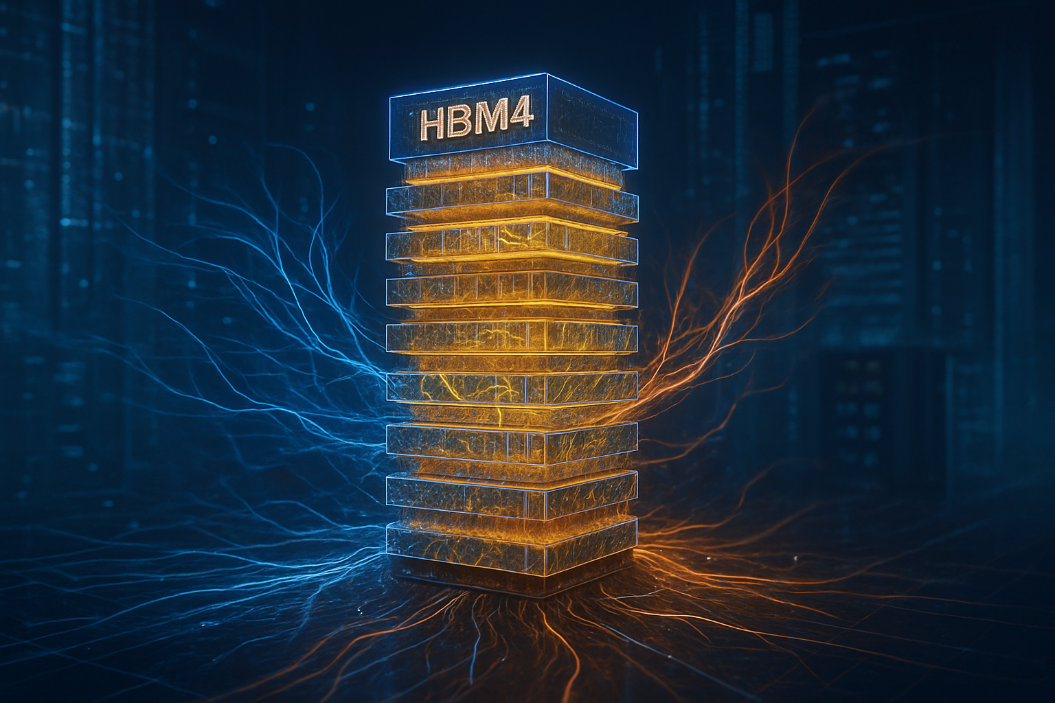
The move to HBM4 represents the most significant architectural evolution in memory technology since the inception of the HBM standard. Unlike HBM3E, which utilized a 1024-bit interface, HBM4 doubles the bus width to a 2048-bit I/O interface. This allows for staggering data throughput of over 2.0 TB/s per stack at lower clock speeds, drastically improving power efficiency—a critical factor for data centers already pushed to their thermal limits. SK Hynix’s HBM4 utilizes a "custom HBM" (cHBM) approach, where the traditional DRAM base die is replaced with a logic die manufactured using TSMC’s (NYSE: TSM) 12nm and 5nm processes. This integration allows for memory controllers and physical layer (PHY) functions to be embedded directly into the stack, reducing latency by an estimated 20%.
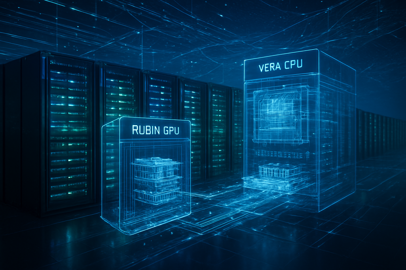
NVIDIA’s "Vera Rubin" platform is designed to take full advantage of these technical leaps. The platform features the new Vera CPU—powered by 88 custom-designed Armv9.2 "Olympus" cores—and the Rubin GPU, which boasts 288GB of HBM4 memory per unit. This configuration provides a 5x increase in AI inference performance compared to the previous Blackwell architecture. Industry experts have noted that SK Hynix’s ability to mass-produce 16-high HBM4 modules, which thin individual DRAM dies to just 30 micrometers to maintain a standard 775-micrometer height limit, was the "killer app" that secured the NVIDIA contract.
The success of SK Hynix is deeply intertwined with its "One Team" alliance with TSMC. By leveraging TSMC’s advanced packaging and logic processes for the HBM4 base die, SK Hynix has solved complex heat and signaling issues that have reportedly hampered its rivals. Initial reactions from the AI research community suggest that the HBM4-equipped Rubin systems will be the first to realistically support the real-time training of trillion-parameter models without the prohibitive energy costs associated with current-gen hardware.
Market Dominance and the Competitive Fallout
The implications for the competitive landscape are profound. For the fiscal year 2025, SK Hynix reported a staggering annual operating profit of 47.2 trillion won, edging out Samsung’s 43.6 trillion won. This reversal of fortunes highlights a fundamental change in the memory industry: value is no longer in sheer volume, but in high-performance specialization. While Samsung still leads in total DRAM production, its late entry into the HBM4 validation process allowed SK Hynix to capture the most profitable segment of the market. Although Samsung reportedly passed NVIDIA's quality tests in January 2026 and plans to begin mass production in February, it finds itself fighting for the remaining 30% of the Rubin supply chain.
Micron Technology (NASDAQ: MU) remains a formidable third player, having successfully delivered 16-high HBM4 samples to NVIDIA and claiming that its 2026 capacity is already "pre-sold." However, Micron lacks the massive production scale of its Korean rivals. Market share projections for 2026 now place SK Hynix at 54% of the global HBM market, with Samsung at 28% and Micron at 18%. This dominance gives SK Hynix unprecedented leverage over pricing and roadmap alignment with the world’s leading AI chipmaker.
Startups and smaller AI labs may feel the pinch of this consolidation. With SK Hynix’s entire 2026 HBM4 capacity already reserved by NVIDIA and a handful of hyperscalers like Google and AWS, the "compute divide" is expected to widen. Companies without pre-existing supply agreements may face multi-month lead times or exorbitant secondary-market pricing for the Rubin-based systems necessary to remain competitive in the frontier model race.
Wider Significance in the AI Landscape
The emergence of SK Hynix as a specialized powerhouse signals a broader trend in the AI landscape: the "logic-ization" of memory. As AI models become more data-hungry, the bottleneck has shifted from raw compute power to the speed at which data can be fed into the processor. By integrating logic functions into the memory stack via HBM4, the industry is moving toward a more holistic, system-on-package (SoP) approach to hardware design. This effectively blurs the line between memory and processing, a milestone that some experts believe is essential for achieving Artificial General Intelligence (AGI).
Furthermore, the "Vera Rubin" platform’s emphasis on power efficiency reflects the industry's response to mounting environmental and regulatory concerns. As global data center energy consumption continues to skyrocket, the 30% power savings offered by HBM4’s wider, slower interface are no longer a luxury but a requirement for future scaling. This transition matches the trajectory of previous AI breakthroughs, such as the shift from CPUs to GPUs, by prioritizing specialized architectures over general-purpose flexibility.
However, this concentration of power in the hands of a few—NVIDIA, SK Hynix, and TSMC—raises concerns regarding supply chain resilience. The "Vera Rubin" platform's reliance on this specific trifecta of companies creates a single point of failure for the global AI economy. Any geopolitical tension or manufacturing hiccup within this tightly coupled ecosystem could stall AI development globally, prompting calls from some Western governments for a more diversified domestic HBM supply chain.
Future Developments and the Road to Rubin Ultra
Looking ahead, the road is already paved for the next iteration of memory technology. While HBM4 is only just reaching the market, SK Hynix and NVIDIA are already discussing "HBM4E," which is expected to debut with the "Rubin Ultra" variant in late 2027. This successor is anticipated to scale to 1TB of memory per GPU, further pushing the boundaries of what is possible in large-scale inference and multi-modal AI.
The immediate challenge for SK Hynix will be maintaining its yield rates as it scales 16-layer production. Thining silicon dies to 30 micrometers is a feat of engineering that leaves little room for error. If the company can maintain its current 70% share while improving yields, it could potentially reach operating margins that rival software companies. Meanwhile, the AI industry is watching closely for the emergence of "Processing-in-Memory" (PIM), where AI calculations are performed directly within the HBM stack. This could be the next major frontier for the SK Hynix-TSMC partnership.
Summary of the New Silicon Hierarchy
The report that SK Hynix has secured 70% of the HBM4 orders for NVIDIA’s Vera Rubin platform cements a new hierarchy in the semiconductor world. By pivoting early and aggressively toward high-bandwidth memory and forming a strategic "One Team" with TSMC, SK Hynix has transformed from a commodity memory supplier into a foundational pillar of the AI revolution. Its record 2025 profits and the displacement of Samsung as the profitability leader underscore a permanent shift in how value is captured in the silicon industry.
As we move through the first quarter of 2026, the focus will shift to the real-world performance of the Vera Rubin systems. The ability of SK Hynix to deliver on its massive order book will determine the pace of AI advancement for the next two years. For now, the "AI Memory King" wears the crown securely, having successfully navigated the transition to HBM4 and solidified its status as the primary engine behind the exascale AI era.
This content is intended for informational purposes only and represents analysis of current AI developments.
TokenRing AI delivers enterprise-grade solutions for multi-agent AI workflow orchestration, AI-powered development tools, and seamless remote collaboration platforms.
For more information, visit https://www.tokenring.ai/.