Tag: Nvidia

  • The Great Decoupling: How Cloud Giants are Breaking the NVIDIA Monopoly with Custom 3nm Silicon

    The Great Decoupling: How Cloud Giants are Breaking the NVIDIA Monopoly with Custom 3nm Silicon

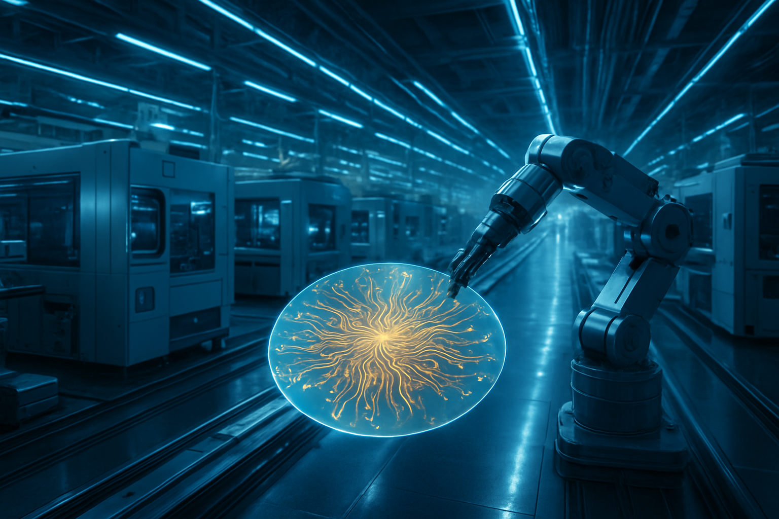
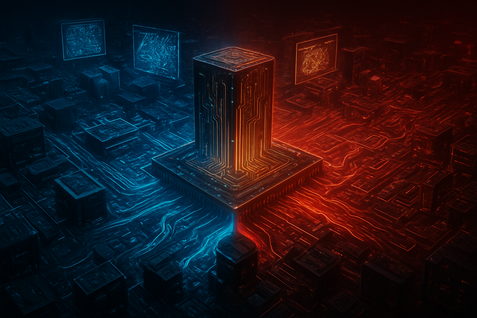
    As of January 2026, the artificial intelligence industry has reached a historic turning point dubbed "The Great Decoupling." For the last several years, the world’s largest cloud providers—Alphabet Inc. (NASDAQ: GOOGL), Amazon.com Inc. (NASDAQ: AMZN), and Microsoft Corp. (NASDAQ: MSFT)—were locked in a fierce bidding war for NVIDIA Corp. (NASDAQ: NVDA) hardware, effectively funding the GPU giant’s meteoric rise to a multi-trillion dollar valuation. However, new data from early 2026 reveals a structural shift: hyperscalers are no longer just buyers; they are now NVIDIA's most formidable architectural rivals.

    By vertically integrating their own hardware, these tech titans are successfully bypassing the "NVIDIA tax"—the massive 70-75% gross margins commanded by the Blackwell and subsequent Ruby GPU architectures. The deployment of custom Application-Specific Integrated Circuits (ASICs) like Google’s TPU v7, Amazon’s unified Trainium3, and Microsoft’s newly launched Maia 200 series has begun to reshape the economics of AI. This shift marks the end of the "Training Era," where general-purpose GPUs were king, and the beginning of the "Agentic Inference Era," where specialized, cost-efficient silicon is the prerequisite for scaling autonomous AI agents to billions of users.

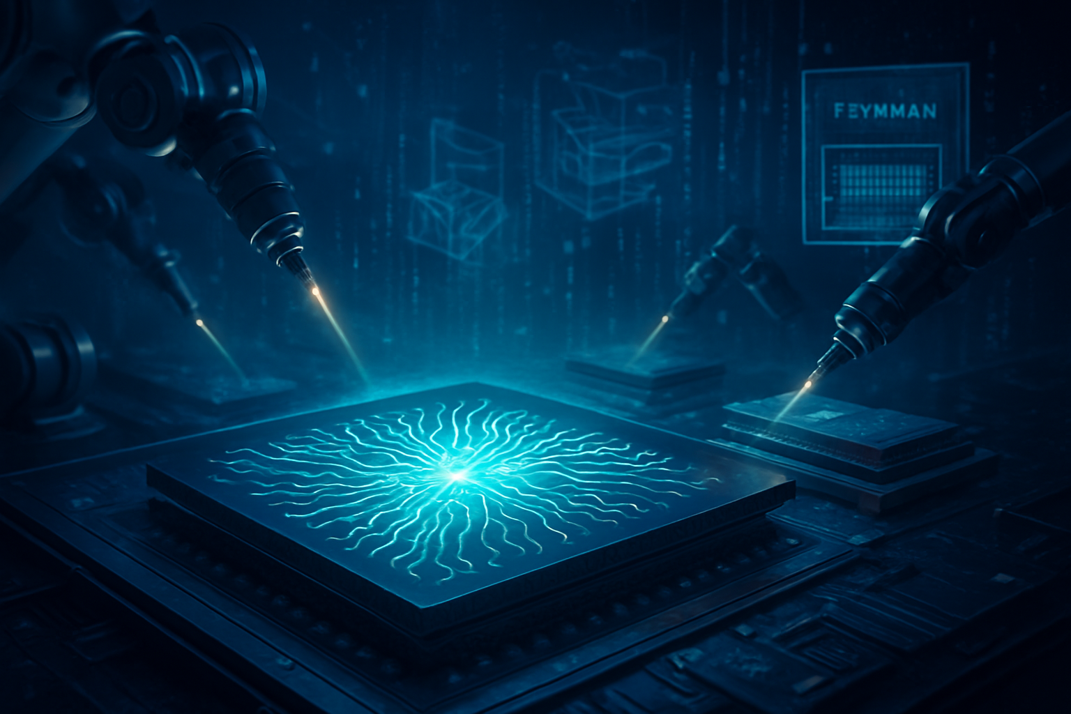
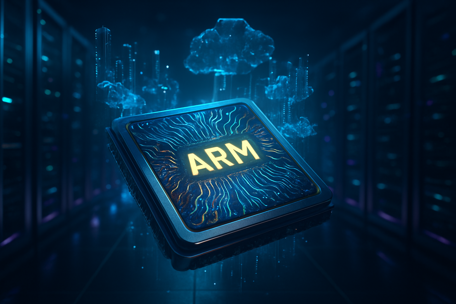
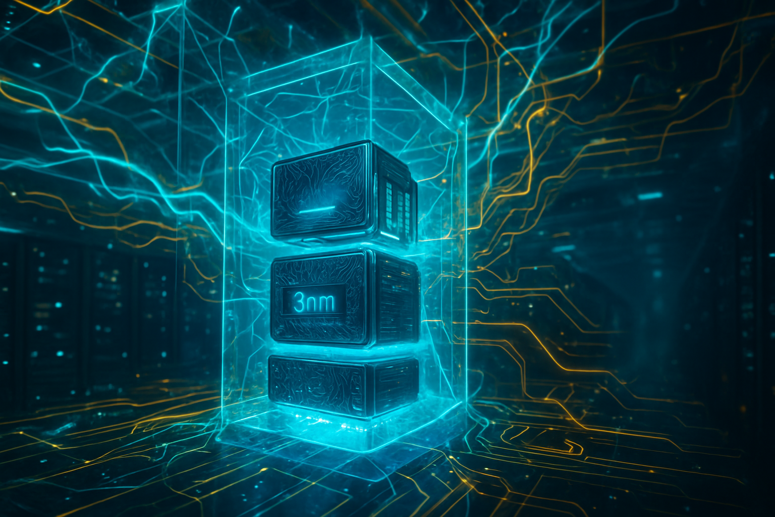
    The 3nm Arms Race: TPU v7, Trainium3, and Maia 200

    The technical specifications of the 2026 silicon crop highlight a move toward extreme specialization. Google recently began the phased rollout of its TPU v7 series, specifically the v7E flagship, targeted at high-performance "reasoning" models. This follows the massive success of its TPU v6 (Trillium) chips, which reached a projected shipment volume of 1.6 million units this year. The v7 architecture integrates Google’s custom Axion ARM-based CPUs as "head nodes," creating a vertically optimized stack that Google claims offers 67% better energy efficiency than previous generations.

    Amazon has taken a different approach by consolidating its hardware roadmap. At re:Invent 2025, AWS unveiled Trainium3, its first chip built on a cutting-edge 3nm process. In a surprising strategic pivot, AWS has halted the standalone development of its Inferentia line, merging training and inference capabilities into the single Trainium3 architecture. This unified silicon delivers 4.4x the compute performance of its predecessor and powers "UltraServers" that house 144 chips, allowing for clusters that scale up to 1 million interconnected processors via the proprietary NeuronSwitch fabric.

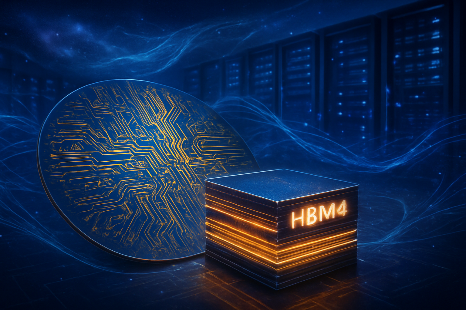
    Microsoft, meanwhile, has hit its stride with the Maia 200, announced on January 26, 2026. Unlike the limited rollout of the first-generation Maia, the 200 series is already live in major data center hubs like US Central (Iowa). Built on TSMC 3nm technology with a staggering 216GB of HBM3e memory, the Maia 200 is specifically tuned for the FP4 and FP8 precision formats required by OpenAI’s latest GPT-5.2 models. Early benchmarks suggest the Maia 200 delivers 3x the FP4 throughput of Amazon’s Trainium3, positioning it as the most performant first-party inference chip in the cloud today.

    Bypassing the "NVIDIA Tax" and Reshaping the Market

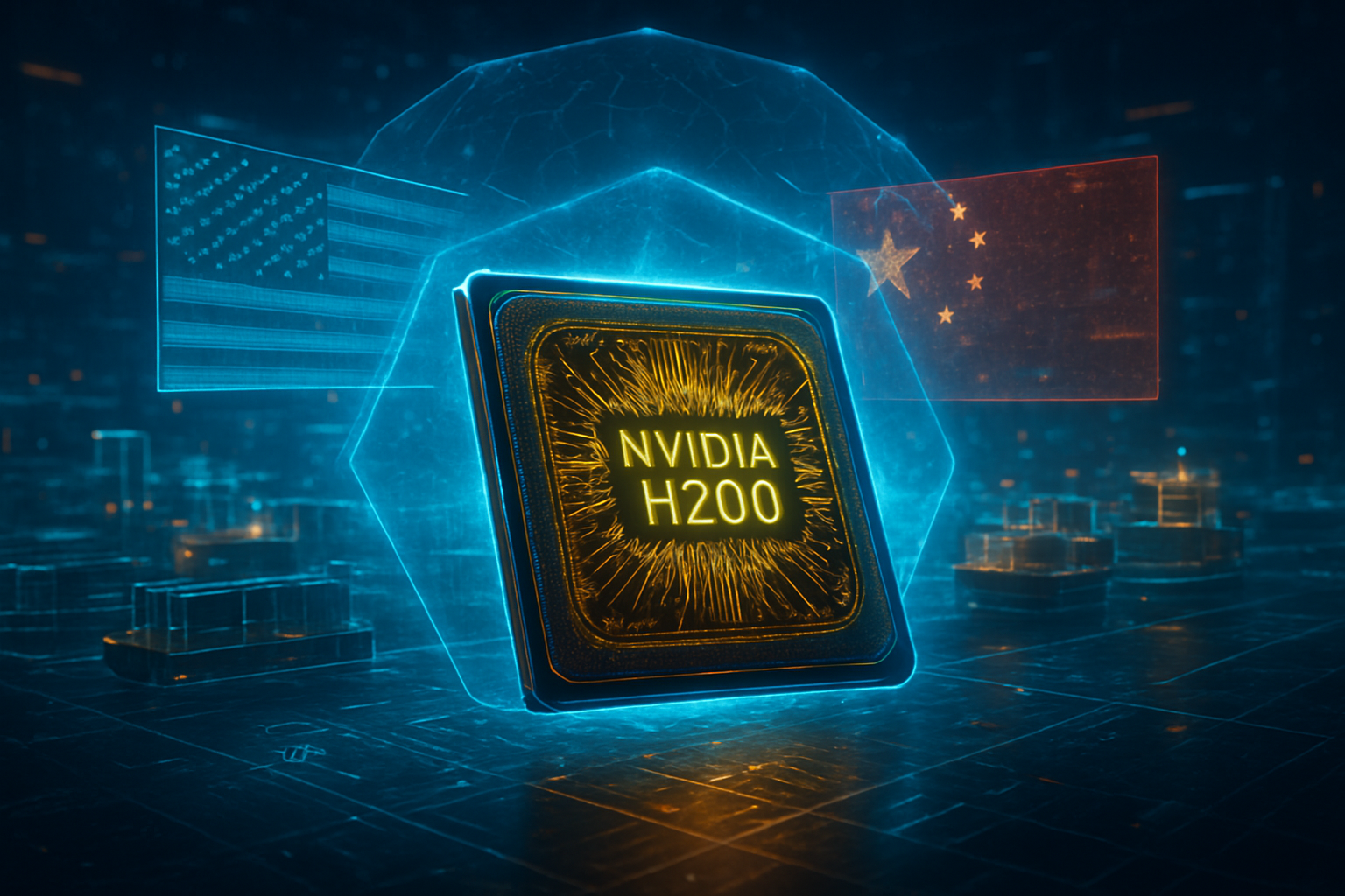
    The strategic driver behind this silicon explosion is purely financial. An individual NVIDIA Blackwell (B200) card currently commands between $30,000 and $45,000, creating an unsustainable cost structure for cloud providers seeking to provide affordable AI at scale. By moving to in-house designs, hyperscalers report a 30% to 40% reduction in Total Cost of Ownership (TCO). Microsoft recently noted that Maia 200 provides 30% better performance-per-dollar than any commercial hardware currently available in the Azure fleet.

    This trend is causing a significant divergence in the semiconductor market. While NVIDIA still dominates the revenue share of the AI sector due to its high ASPs (Average Selling Prices), custom ASICs are winning the volume war. According to late 2025 reports from TrendForce, custom AI processor shipments grew by 44% over the past year, far outpacing the 16% growth seen in traditional GPUs. Google’s TPU ecosystem alone now accounts for over 52% of the global AI Server ASIC volume.

    For NVIDIA, the challenge is no longer just manufacturing enough chips, but defending its "moat." Hyperscalers are developing proprietary interconnects to avoid being locked into NVIDIA’s NVLink ecosystem. By controlling the silicon, the fabric, and the software stack (such as AWS’s Neuron SDK or Google’s JAX-optimized compilers), cloud giants are creating "walled garden" architectures where their own chips perform better for their specific internal workloads than NVIDIA's general-purpose alternatives.

    The Shift to the Agentic Inference Era

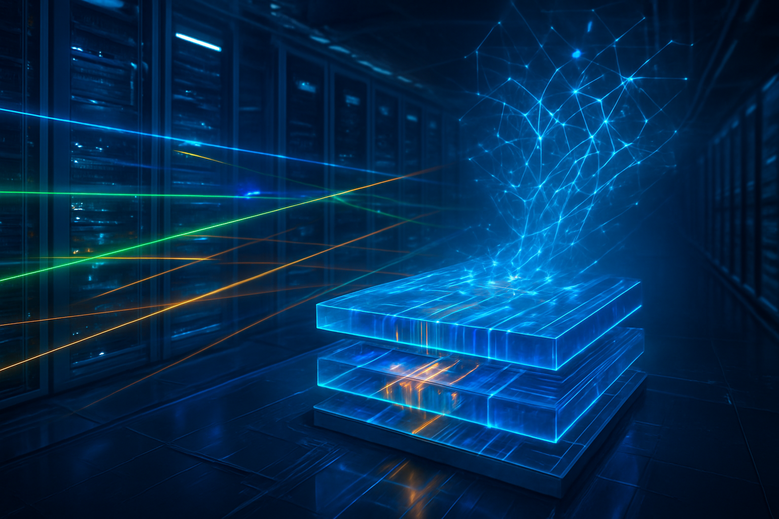
    The broader significance of this silicon shift lies in the changing nature of AI workloads. We are moving away from the era of "frontier training," which required the massive raw power of tens of thousands of GPUs linked together for months. We are now entering the Agentic Inference Era, where the primary cost and technical challenge is running millions of autonomous agents simultaneously. These agents require "fast" and "cheap" tokens, which favors the streamlined, low-latency architectures of ASICs over the more complex, power-hungry instruction sets of traditional GPUs.

    Even companies without their own public cloud, like Meta Platforms Inc. (NASDAQ: META), are following this playbook. Meta’s MTIA v2 is currently powering the massive ranking and recommendation engines for Facebook and Instagram. However, indicating how competitive the market has become, reports suggest Meta is negotiating to purchase Google TPUs by 2027 to further diversify its infrastructure. Meta remains NVIDIA’s largest customer with over 1.3 million GPUs, but the "hybrid" strategy of using custom silicon for high-volume tasks is becoming the industry standard.

    This movement toward sovereign silicon also addresses supply chain vulnerabilities. By designing their own chips, hyperscalers can secure direct long-term contracts with foundries like TSMC, bypassing the allocation bottlenecks that have plagued the industry since 2023. This "silicon sovereignty" allows for more predictable product cycles and the ability to customize hardware for emerging model architectures, such as State Space Models (SSMs) or Liquid Neural Networks, which may not run optimally on standard GPU hardware.

    The Road to 2nm and Beyond

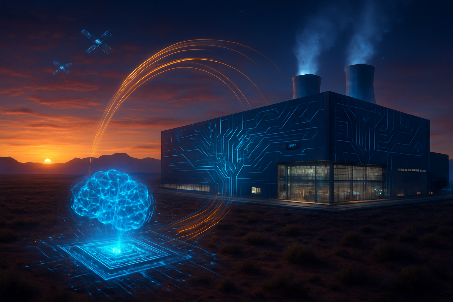
    Looking ahead to 2027 and 2028, the battle for silicon supremacy will move to the 2nm process node. Experts predict that the next generation of custom chips will incorporate integrated optical interconnects, allowing for "optical TBU" (Tensor Processing Units) that use light instead of electricity for chip-to-chip communication, drastically reducing power consumption. This will be critical as data centers face increasing scrutiny over their massive energy footprints.

    We also expect to see these custom chips move "to the edge." As the need for privacy and low latency grows, cloud giants may begin licensing their silicon designs for use in on-premise hardware or specialized "AI appliances." The challenge remains the software; while NVIDIA’s CUDA remains the gold standard for developers, the massive investment by AWS and Google into making their compilers "transparent" is slowly eroding CUDA’s dominance. Analysts project that by 2028, custom ASIC shipments will surpass data center GPU shipments for the first time in history.

    A New Hierarchy in the AI Stack

    The trend of custom silicon marks the most significant architectural shift in computing since the transition from mainframe to client-server. The "Great Decoupling" of 2026 has proven that the world’s largest tech companies are no longer willing to outsource the most critical component of their infrastructure to a single vendor. By owning the silicon, Google, Amazon, and Microsoft have secured their margins and their futures.

    As we look toward the middle of the decade, the industry's focus will shift from "who has the most GPUs" to "who has the most efficient tokens." The winner of the AI race will likely be the company that can provide the highest "intelligence-per-watt," a metric that is now firmly in the hands of the custom silicon designers. In the coming months, keep a close eye on the performance benchmarks of the first GPT-5.2 models running on Maia 200—they will be the ultimate litmus test for whether proprietary hardware can truly outshine the industry’s favorite GPU.


    This content is intended for informational purposes only and represents analysis of current AI developments.

    TokenRing AI delivers enterprise-grade solutions for multi-agent AI workflow orchestration, AI-powered development tools, and seamless remote collaboration platforms.
    For more information, visit https://www.tokenring.ai/.

  • The Great Re-Shoring: US CHIPS Act Enters High-Volume Era as $30 Billion Funding Hits the Silicon Heartland

    The Great Re-Shoring: US CHIPS Act Enters High-Volume Era as $30 Billion Funding Hits the Silicon Heartland

    PHOENIX, AZ — January 28, 2026 — The "Silicon Desert" has officially bloomed. Marking the most significant shift in the global technology supply chain in four decades, the U.S. Department of Commerce today announced that the execution of the CHIPS and Science Act has reached its critical "High-Volume Manufacturing" (HVM) milestone. With over $30 billion in finalized federal awards now flowing into the coffers of industry titans, the massive mega-fabs of Intel, TSMC, and Samsung are no longer mere construction sites of steel and concrete; they are active, revenue-generating engines of American economic and national security.

    In early 2026, the domestic semiconductor landscape has been fundamentally redrawn. In Arizona, TSMC (NYSE: TSM) and Intel Corporation (Nasdaq: INTC) have both reached HVM status on leading-edge nodes, while Samsung Electronics (KRX: 005930) prepares to bring its Texas-based 2nm capacity online to complete a trifecta of domestic advanced logic production. As the first "Made in USA" 1.8nm and 4nm chips begin shipping to customers like Apple (Nasdaq: AAPL) and NVIDIA (Nasdaq: NVDA), the era of American chip dependence on East Asian fabs has begun its slow, strategic sunset.

    The Angstrom Era Arrives: Inside the Mega-Fabs

    The technical achievement of the last 24 months is centered on Intel’s Ocotillo campus in Chandler, Arizona, where Fab 52 has officially achieved High-Volume Manufacturing on the Intel 18A (1.8-nanometer) node. This milestone represents more than just a successful ramp; it is the debut of PowerVia backside power delivery and RibbonFET gate-all-around (GAA) transistors at scale—technologies that have allowed Intel to reclaim the process leadership crown it lost nearly a decade ago. Early yield reports suggest 18A is performing at or above expectations, providing the backbone for the new Panther Lake and Clearwater Forest AI-optimized processors.

    Simultaneously, TSMC’s Fab 1 in Phoenix has successfully stabilized its 4nm (N4P) production line, churning out 20,000 wafers per month. While this node is not the "bleeding edge" currently produced in Hsinchu, it is the workhorse for current-generation AI accelerators and high-performance computing (HPC) chips. The significance lies in the geographical proximity: for the first time, an AMD (Nasdaq: AMD) or NVIDIA chip can be designed in California, manufactured in Arizona, and packaged in a domestic advanced facility, drastically reducing the "transit risk" that has haunted the industry since the 2021 supply chain crisis.

    In the "Silicon Forest" of Oregon, Intel’s D1X expansion has transitioned into a full-scale High-NA EUV (Extreme Ultraviolet) lithography center. This facility is currently the only site in the world operating the newest generation of ASML tools at production density, serving as the blueprint for the massive "Silicon Heartland" project in Ohio. While the Licking County, Ohio complex has faced well-documented delays—now targeting a 2030 production start—the shell completion of its first two fabs in early 2026 serves as a strategic reserve for the next decade of American silicon dominance.

    Shifting the Power: Market Impact and the AI Advantage

    The market implications of these HVM milestones are profound. For years, the AI revolution led by Microsoft (Nasdaq: MSFT) and Alphabet (Nasdaq: GOOGL) was bottlenecked by a single point of failure: the Taiwan Strait. By January 2026, that bottleneck has been partially bypassed. Leading-edge AI startups now have the option to secure "Sovereign AI" capacity—chips manufactured entirely on U.S. soil—a requirement that is increasingly becoming standard in Department of Defense and high-security enterprise contracts.

    Which companies stand to benefit most? Intel Foundry is the clear winner in the near term. By opening its 18A node to third-party customers and securing a 9.9% equity stake from the U.S. government as part of a "national champion" model, Intel has transformed from a struggling IDM into a formidable domestic foundry rival to TSMC. Conversely, TSMC has utilized its $6.6 billion in CHIPS Act grants to solidify its relationship with its largest U.S. customers, proving it can successfully replicate its legendary "Taiwan Ecosystem" in the harsh climate of the American Southwest.

    However, the transition is not without friction. Industry analysts at Nomura and SEMI note that U.S.-made chips currently carry a 20–30% "resiliency premium" due to higher labor and operational costs. While the $30 billion in subsidies has offset initial capital expenditures, the long-term market positioning of these fabs will depend on whether the U.S. government introduces further protectionist measures, such as the widely discussed 100% tariff on mature-node legacy chips from non-allied nations, to ensure the new mega-fabs remain price-competitive.

    The Global Chessboard: A New AI Reality

    The broader significance of the CHIPS Act execution cannot be overstated. We are witnessing the first successful "industrial policy" initiative in the U.S. in recent history. In 2022, the U.S. produced 0% of the world’s most advanced logic chips; by the close of 2025, that number has climbed to 15%. This shift fits into a wider trend of "techno-nationalism," where AI hardware is viewed not just as a commodity, but as the foundational layer of national power.

    Comparison to previous milestones, like the 1950s interstate highway system or the 1960s Space Race, are frequent among policy experts. Yet, the semiconductor race is arguably more complex. The potential concerns center on "subsidy addiction." If the $30 billion in funding is not followed by sustained private investment and a robust talent pipeline—Arizona alone faces a 3,000-engineer shortfall this year—the mega-fabs risk becoming "white elephants" that require perpetual government lifelines.

    Furthermore, the environmental impact of these facilities has sparked local debates. The Phoenix mega-fabs consume millions of gallons of water daily, a challenge that has forced Intel and TSMC to pioneer world-leading water reclamation technologies that recycle over 90% of their intake. These environmental breakthroughs are becoming as essential to the semiconductor industry as the lithography itself.

    The Horizon: 2nm and Beyond

    Looking forward to the remainder of 2026 and 2027, the focus shifts from "production" to "scaling." Samsung’s Taylor, Texas facility is slated to begin its trial runs for 2nm production in late 2026, aiming to steal the lead for next-generation AI processors used in autonomous vehicles and humanoid robotics. Meanwhile, TSMC is already breaking ground on its third Phoenix fab, which is designated for the 2nm era by 2028.

    The next major challenge will be the "packaging gap." While the U.S. has successfully re-shored the making of chips, the assembly and packaging of those chips still largely occur in Malaysia, Vietnam, and Taiwan. Experts predict that the next phase of CHIPS Act funding—or a potential "CHIPS 2.0" bill—will focus almost exclusively on advanced back-end packaging to ensure that a chip never has to leave U.S. soil from sand to server.

    Summary: A Historic Pivot for the Industry

    The early 2026 HVM milestones in Arizona, Oregon, and the construction progress in Ohio represent a historic pivot in the story of artificial intelligence. The execution of the CHIPS Act has moved from a legislative gamble to an operational reality. We have entered an era where "Made in America" is no longer a slogan for heavy machinery, but a standard for the most sophisticated nanostructures ever built by humanity.

    As we watch the first 18A wafers roll off the line in Ocotillo, the takeaway is clear: the U.S. has successfully bought its way back into the semiconductor game. The long-term impact will be measured in the stability of the AI market and the security of the digital world. For the coming months, keep a close eye on yield rates and customer announcements; the hardware that will power the 2030s is being born today in the American heartland.


    This content is intended for informational purposes only and represents analysis of current AI developments.

    TokenRing AI delivers enterprise-grade solutions for multi-agent AI workflow orchestration, AI-powered development tools, and seamless remote collaboration platforms.
    For more information, visit https://www.tokenring.ai/.

  • The 2nm Epoch: How TSMC’s Silicon Shield Redefines Global Security in 2026

    The 2nm Epoch: How TSMC’s Silicon Shield Redefines Global Security in 2026

    HSINCHU, Taiwan — As the world enters the final week of January 2026, the semiconductor industry has officially crossed the threshold into the "Angstrom Era." Taiwan Semiconductor Manufacturing Company (NYSE: TSM), the world's most critical foundry, has formally announced the commencement of high-volume manufacturing (HVM) for its groundbreaking 2-nanometer (N2) process technology. This milestone does more than just promise faster smartphones and more capable AI; it reinforces Taiwan’s "Silicon Shield," a unique geopolitical deterrent that renders the island indispensable to the global economy and, by extension, global security.

    The activation of 2nm production at Fab 20 in Baoshan and Fab 22 in Kaohsiung comes at a delicate moment in international relations. As the United States and Taiwan finalize a series of historic trade accords under the "US-Taiwan Initiative on 21st-Century Trade," the 2nm node emerges as the ultimate bargaining chip. With NVIDIA (NASDAQ: NVDA) and Apple (NASDAQ: AAPL) having already secured the lion's share of this new capacity, the world’s reliance on Taiwanese silicon has reached an unprecedented peak, solidifying the island’s role as the "Geopolitical Anchor" of the Pacific.

    The Nanosheet Revolution: Inside the 2nm Breakthrough

    The shift to the 2nm node represents the most significant architectural overhaul in semiconductor manufacturing in over a decade. For the first time, TSMC has transitioned away from the long-standing FinFET (Fin Field-Effect Transistor) structure to a Nanosheet Gate-All-Around (GAAFET) architecture. In this design, the gate wraps entirely around the channel on all four sides, providing superior control over current flow, drastically reducing leakage, and allowing for lower operating voltages. Technical specifications released by TSMC indicate that the N2 node delivers a 10–15% performance boost at the same power level, or a staggering 25–30% reduction in power consumption compared to the previous 3nm (N3E) generation.

    Industry experts have been particularly stunned by TSMC’s initial yield rates. Reports from within the Hsinchu Science Park suggest that logic test chip yields for the N2 node have stabilized between 70% and 80%—a remarkably high figure for a brand-new architecture. This maturity stands in stark contrast to earlier struggles with the 3nm ramp-up and places TSMC in a dominant position compared to its nearest rivals. While Samsung (KRX: 005930) was the first to adopt GAA technology at the 3nm stage, its 2nm (SF2) yields are currently estimated to hover around 50%, making it difficult for the South Korean giant to lure high-volume customers away from the Taiwanese foundry.

    Meanwhile, Intel (NASDAQ: INTC) has officially entered the fray with its own 18A process, which launched in high volume this week for its "Panther Lake" CPUs. While Intel has claimed the architectural lead by being the first to implement backside power delivery (PowerVia), TSMC’s conservative decision to delay backside power until its A16 (1.6nm) node—expected in late 2026—appears to have paid off in terms of manufacturing stability and predictable scaling for its primary customers.

    The Concentration of Power: Who Wins the 2nm Race?

    The immediate beneficiaries of the 2nm era are the titans of the AI and mobile industries. Apple has reportedly booked more than 50% of TSMC’s initial 2nm capacity for its upcoming A20 and M6 chips, ensuring that the next generation of iPhones and MacBooks will maintain a significant lead in on-device AI performance. This strategic lock-on capacity creates a massive barrier to entry for competitors, who must now wait for secondary production windows or settle for previous-generation nodes.

    In the data center, NVIDIA is the primary benefactor. Following the announcement of its "Rubin" architecture at CES 2026, NVIDIA CEO Jensen Huang confirmed that the Rubin GPUs will leverage TSMC’s 2nm process to deliver a 10x reduction in inference token costs for massive AI models. The strategic alliance between TSMC and NVIDIA has effectively created a "hardware moat" that makes it nearly impossible for rival AI labs to achieve comparable efficiency without Taiwanese silicon. AMD (NASDAQ: AMD) is also waiting in the wings, with its "Zen 6" architecture slated to be the first x86 platform to move to the 2nm node by the end of the year.

    This concentration of advanced manufacturing power has led to a reshuffling of market positioning. TSMC now holds an estimated 65% of the total foundry market share, but more importantly, it holds nearly 100% of the market for the chips that power the "Physical AI" and autonomous reasoning models defining 2026. For major tech giants, the strategic advantage is clear: those who do not have a direct line to Hsinchu are increasingly finding themselves at a competitive disadvantage in the global AI race.

    The Silicon Shield: Geopolitical Anchor or Growing Liability?

    The "Silicon Shield" theory posits that Taiwan’s dominance in high-end chips makes it too valuable to the world—and too dangerous to damage—for any conflict to occur. In 2026, this shield has evolved into a "Geopolitical Anchor." Under the newly signed 2026 Accords of the US-Taiwan Initiative on 21st-Century Trade, the two nations have formalized a "pay-to-stay" model. Taiwan has committed to a staggering $250 billion in direct investments into U.S. soil—specifically for advanced fabs in Arizona and Ohio—in exchange for Most-Favored-Nation (MFN) status and guaranteed security cooperation.

    However, the shield is not without its cracks. A growing "hollowing out" debate in Taipei suggests that by moving 2nm and 3nm production to the United States, Taiwan is diluting its strategic leverage. While the U.S. is gaining "chip security," the reality of manufacturing in 2026 remains complex. Data shows that building and operating a fab in the U.S. costs nearly double that of a fab in Taiwan, with construction times taking 38 months in the U.S. compared to just 20 months in Taiwan. Furthermore, the "Equipment Leveler" effect—where 70% of a wafer's cost is tied to expensive machinery from ASML (NASDAQ: ASML) and Applied Materials (NASDAQ: AMAT)—means that even with U.S. subsidies, Taiwanese fabs remain the more profitable and efficient choice.

    As of early 2026, the global economy is so deeply integrated with Taiwanese production that any disruption would result in a multi-trillion-dollar collapse. This "mutually assured economic destruction" remains the strongest deterrent against aggression in the region. Yet, the high costs and logistical complexities of "friend-shoring" continue to be a point of friction in trade negotiations, as the U.S. pushes for more domestic capacity while Taiwan seeks to keep its R&D "motherboard" firmly at home.

    The Road to 1.6nm and Beyond

    The 2nm milestone is merely a stepping stone toward the next frontier: the A16 (1.6nm) node. TSMC has already previewed its roadmap for the second half of 2026, which will introduce the "Super Power Rail." This technology will finally bring backside power delivery to TSMC’s portfolio, moving the power routing to the back of the wafer to free up space on the front for more transistors and more complex signal paths. This is expected to be the key enabler for the next generation of "Reasoning AI" chips that require massive electrical current and ultra-low latency.

    Near-term developments will focus on the rollout of the N2P (Performance) node, which is expected to enter volume production by late summer. Challenges remain, particularly in the talent pipeline. To meet the demands of the 2nm ramp-up, TSMC has had to fly thousands of engineers from Taiwan to its Arizona sites, highlighting a "tacit knowledge" gap in the American workforce that may take years to bridge. Experts predict that the next eighteen months will be a period of "workforce integration," as the U.S. tries to replicate the "Science Park" cluster effect that has made Taiwan so successful.

    A Legacy in Silicon: Final Thoughts

    The official start of 2nm mass production in January 2026 marks a watershed moment in the history of artificial intelligence and global politics. TSMC has not only maintained its technological lead through a risky architectural shift to GAAFET but has also successfully navigated the turbulent waters of international trade to remain the indispensable heart of the tech industry.

    The significance of this development cannot be overstated; the 2nm era is the foundation upon which the next decade of AI breakthroughs will be built. As we watch the first N2 wafers roll off the line this month, the world remains tethered to a small island in the Pacific. The "Silicon Shield" is stronger than ever, but as the costs of maintaining this lead continue to climb, the balance between global security and domestic industrial policy will be the most important story to follow for the remainder of 2026.


    This content is intended for informational purposes only and represents analysis of current AI developments.

    TokenRing AI delivers enterprise-grade solutions for multi-agent AI workflow orchestration, AI-powered development tools, and seamless remote collaboration platforms.
    For more information, visit https://www.tokenring.ai/.

  • NVIDIA Breaks TSMC Monopoly: Strategic Move to Intel Foundry for Future “Feynman” AI Chips

    NVIDIA Breaks TSMC Monopoly: Strategic Move to Intel Foundry for Future “Feynman” AI Chips

    In a move that has sent shockwaves through the global semiconductor industry, NVIDIA (NASDAQ: NVDA) has officially confirmed a landmark dual-foundry strategy, marking a historic shift away from its exclusive reliance on TSMC (NYSE: TSM). According to internal reports and supply chain data as of January 2026, NVIDIA is moving the production of its critical I/O (Input/Output) dies for the upcoming "Feynman" architecture to Intel Corporation (NASDAQ: INTC). This transition utilizes Intel’s cutting-edge 14A process node and advanced EMIB packaging technology, signaling a new era of "Made-in-America" AI hardware.

    The announcement comes at a time when the demand for AI compute capacity has outstripped even the most optimistic projections. By integrating Intel Foundry into its manufacturing ecosystem, NVIDIA aims to solve chronic supply chain bottlenecks while simultaneously hedging against growing geopolitical risks in East Asia. The partnership is not merely a tactical pivot but a massive strategic bet, underscored by NVIDIA’s reported $5 billion investment in Intel late last year to secure long-term capacity for its next-generation AI platforms.

    Technical Synergy: 14A Nodes and EMIB Packaging

    The technical core of this partnership centers on the "Feynman" architecture, the planned successor to NVIDIA’s Rubin series. While TSMC will continue to manufacture the high-performance compute dies—the "brains" of the GPU—on its A16 (1.6nm) node, Intel has been tasked with the Feynman I/O die. This component is essential for managing the massive data throughput between the GPU and its memory stacks. NVIDIA is specifically targeting Intel’s 14A node, a 1.4nm-class process that utilizes High-NA EUV (Extreme Ultraviolet) lithography to achieve unprecedented transistor density and power efficiency.

    A standout feature of this collaboration is the use of Intel’s Embedded Multi-die Interconnect Bridge (EMIB) packaging. Unlike the traditional silicon interposers used in TSMC’s CoWoS (Chip-on-Wafer-on-Substrate) technology, EMIB allows for high-speed communication between chiplets using smaller, embedded bridges. This approach offers superior thermal management and significantly higher manufacturing yields for ultra-large AI packages. Experts note that EMIB will be a critical enabler for High Bandwidth Memory 5 (HBM5), allowing the Feynman platform to reach memory bandwidths exceeding 13 TB/s—a requirement for the "Gigawatt-scale" AI data centers currently being planned for 2027 and 2028.

    Furthermore, the Feynman I/O die will benefit from Intel’s PowerVia technology, a form of backside power delivery that separates power routing from the signal layers. This innovation drastically reduces signal interference and voltage drop, which are major hurdles in modern chip design. Initial reactions from the AI research community have been cautiously optimistic, with many noting that this dual-foundry approach provides a much-needed "relief valve" for the industry-wide packaging shortage that has plagued AI scaling for years.

    Market Shakeup: A Lifeline for Intel and a Hedge for NVIDIA

    This strategic pivot is being hailed by Wall Street as a "historic lifeline" for Intel Foundry. Following the confirmation of the partnership, Intel’s stock saw a 5% surge, as investors finally saw the customer validation necessary to justify the company's multi-billion-dollar foundry investments. For NVIDIA, the move provides significant leverage in future pricing negotiations with TSMC, which has reportedly considered aggressive price hikes for its 2nm-class wafers. By qualifying Intel as a primary source for I/O dies, NVIDIA is no longer captive to a single supplier's roadmap or pricing structure.

    The competitive implications for the broader tech sector are profound. Major AI labs and tech giants like Google and Amazon, which have been developing their own custom silicon, may now find themselves competing with a more agile and supply-resilient NVIDIA. If NVIDIA can successfully scale its production across two of the world’s leading foundries, it could effectively "flood the zone" with AI chips, potentially suffocating the market share of smaller startups and rival chipmakers who remain tied solely to TSMC’s overbooked capacity.

    Industry analysts at Morgan Stanley (NYSE: MS) suggest that this move could also pressure AMD and Qualcomm to accelerate their own dual-foundry efforts. The shift signifies that the era of "single-foundry loyalty" is over, replaced by a more complex, multi-sourced supply chain model. While TSMC remains the undisputed leader in pure compute performance, Intel’s emergence as a viable second source for advanced packaging and I/O logic shifts the balance of power back toward domestic manufacturing.

    Geopolitical Resilience and the "Chip Sovereignty" Era

    Beyond the technical and financial metrics, NVIDIA's move into Intel's fabs is deeply intertwined with the current geopolitical landscape. As of early 2026, the push for "chip sovereignty" has become a dominant theme in global trade. Under pressure from the current U.S. administration’s mandates for domestic manufacturing and the looming threat of tariffs on imported high-tech components, NVIDIA’s partnership with Intel allows it to brand its upcoming Feynman chips as "Made in America."

    This diversification serves as a critical hedge against potential instability in the Taiwan Strait. With over 90% of the world's most advanced AI chips currently manufactured in Taiwan, the industry has long lived under a "single point of failure" risk. By shifting 25% of its Feynman production and packaging to Intel's facilities in Arizona and Ohio, NVIDIA is insulating its future revenue from localized geopolitical disruptions. This move mirrors a broader trend where tech giants are prioritizing supply chain resilience over pure cost optimization.

    The broader AI landscape is also shifting from a focus on "nanometer counts" to "packaging efficiency." As Moore’s Law slows down, the ability to stitch together different dies (compute, I/O, and memory) becomes more important than the size of the transistors themselves. The NVIDIA-Intel alliance represents a major milestone in this transition, proving that the future of AI will be defined by how well different specialized components can be integrated into a single, massive system-on-package.

    Looking Ahead: The Road to Feynman 2028

    The road toward the full launch of the Feynman architecture in 2028 is filled with both promise and technical hurdles. In the near term, NVIDIA and Intel will begin risk production and pilot runs of the 14A I/O dies throughout 2026 and 2027. The primary challenge will be Intel's ability to execute at the unprecedented scale NVIDIA requires. Any yield issues or delays in the 14A ramp-up could force NVIDIA to revert back to TSMC, potentially derailing the strategic benefits of the partnership.

    Experts predict that if this collaboration succeeds, it will pave the way for more ambitious joint projects, perhaps even extending to the compute die for future generations. We may also see a rise in "bespoke" AI infrastructure, where NVIDIA designs specific I/O dies tailored for different regions or regulatory environments, manufactured locally to meet data sovereignty laws. The evolution of EMIB technology will be a key metric to watch, as it could eventually surpass the performance of competing interposer-based technologies.

    A New Chapter in the AI Industrial Revolution

    The formalization of the NVIDIA-Intel partnership marks one of the most significant pivots in the history of the semiconductor industry. By breaking the TSMC monopoly on high-end AI manufacturing, NVIDIA has not only secured its own supply chain but has also fundamentally altered the competitive dynamics of the tech world. This move represents a sophisticated blend of technical innovation, market strategy, and geopolitical pragmatism.

    In the coming months, the industry will be watching Intel's 18A and 14A yield reports with intense scrutiny. For NVIDIA, the success of the Feynman architecture will be the ultimate test of this dual-foundry strategy. If successful, this partnership could become the blueprint for the next decade of AI development—one where the world’s most powerful chips are built through global collaboration rather than single-source dependency.


    This content is intended for informational purposes only and represents analysis of current AI developments.

    TokenRing AI delivers enterprise-grade solutions for multi-agent AI workflow orchestration, AI-powered development tools, and seamless remote collaboration platforms. For more information, visit https://www.tokenring.ai/.

  • The Silicon Standoff: Trump’s H200 ‘Taxable Dependency’ Sparking a New Cold War in AI

    The Silicon Standoff: Trump’s H200 ‘Taxable Dependency’ Sparking a New Cold War in AI

    In a month defined by unprecedented policy pivots and high-stakes brinkmanship, the global semiconductor market has been plunged into a state of "logistical limbo." On January 14, 2026, the Trump administration shocked the tech world by granting NVIDIA (NASDAQ: NVDA) a formal license to export the H200 Tensor Core GPU to China—a move that initially signaled a thawing of tech tensions but quickly revealed itself to be a calculated economic maneuver. By attaching a mandatory 25% "Trump Surcharge" and rigorous domestic safety testing requirements to the license, the U.S. has attempted to transform its technological edge into a direct revenue stream for the Treasury.

    However, the "thaw" was met with an immediate and icy "freeze" from Beijing. Within 24 hours of the announcement, Chinese customs officials in Shenzhen and Hong Kong issued a total blockade on H200 shipments, refusing to clear the very hardware their tech giants have spent billions to acquire. This dramatic sequence of events has effectively bifurcated the AI ecosystem, leaving millions of high-end GPUs stranded in transit and forcing a reckoning for the "Silicon Shield" strategy that has long underpinned the delicate peace between the world’s two largest economies.

    The Technical Trap: Security, Surcharges, and the 50% Rule

    The NVIDIA H200, while recently succeeded by the "Blackwell" B200 architecture, remains the gold standard for large-scale AI inference and training. Boasting 141GB of HBM3e memory and a staggering 4.8 TB/s of bandwidth, the H200 is specifically designed to handle the massive parameter counts of the world's most advanced large language models. Under the new January 2026 export guidelines, these chips were not merely shipped; they were subjected to a gauntlet of "Taxable Dependency" conditions. Every H200 bound for China was required to pass through independent, third-party laboratories within the United States for "Safety Verification." This process was designed to ensure that the chips had not been physically modified to bypass performance caps or facilitate unauthorized military applications.

    Beyond the technical hurdles, the license introduced the "Trump Surcharge," a 25% fee on the sales price of every unit, payable directly to the U.S. government. Furthermore, the administration instituted a "50% Rule," which mandates that NVIDIA cannot sell more than half the volume of its U.S. domestic sales to China. This ensures that American firms like Microsoft (NASDAQ: MSFT) and Alphabet (NASDAQ: GOOGL) maintain clear priority access to the best hardware. Initial reactions from the AI research community have been polarized; while some see this as a pragmatic way to leverage American innovation for national gain, others, like the Open Compute Project, warn that these "managed trade" conditions create an administrative nightmare that threatens the speed of global AI development.

    A Corporate Tug-of-War: NVIDIA Caught in the Crossfire

    The fallout from the Chinese customs blockade has been felt instantly across the balance sheets of major tech players. For NVIDIA, the H200 was intended to be a major revenue driver for the first quarter of 2026, potentially recapturing billions in "lost" Chinese revenue. The blockade, however, has paralyzed their supply chain. Suppliers in the region who manufacture specialized circuit boards and cooling systems specifically for the H200 architecture were forced to halt production almost immediately after Beijing "urged" Chinese tech giants to look elsewhere.

    Major Chinese firms, including Alibaba (NYSE: BABA), Tencent (HKEX: 0700), and ByteDance, find themselves in an impossible position. While their engineering teams are desperate for NVIDIA hardware to keep pace with Western breakthroughs in generative video and autonomous reasoning, they are being summoned by Beijing to prioritize "Silicon Sovereignty." This mandate effectively forces a transition to domestic alternatives like Huawei’s Ascend series. For U.S.-based hyperscalers, this development offers a temporary strategic advantage, as their competitors in the East are now artificially capped by hardware limitations, yet the disruption to the global supply chain—where many NVIDIA components are still manufactured in Asia—threatens to raise costs for everyone.

    Weaponizing the Silicon Shield

    The current drama represents a fundamental evolution of the "Silicon Shield" theory. Traditionally, this concept suggested that Taiwan’s dominance in chip manufacturing, led by Taiwan Semiconductor Manufacturing Company (NYSE: TSM), protected it from conflict because a disruption would be too costly for both the U.S. and China. In January 2026, we are seeing the U.S. attempt to "weaponize" this shield. By allowing exports under high-tax conditions, the Trump administration is testing whether China’s need for AI dominance is strong enough to swallow a "taxable dependency" on American-designed silicon.

    This strategy fits into a broader trend of "techno-nationalism" that has dominated the mid-2020s. By routing chips through U.S. labs and imposing a volume cap, the U.S. is not just protecting national security; it is asserting control over the global pace of AI progress. China’s retaliatory blockade is a signal that it would rather endure a period of "AI hunger" than accept a subordinate role in a tiered technology system. This standoff highlights the limits of the Silicon Shield; while it may prevent physical kinetic warfare, it has failed to prevent a "Total Trade Freeze" that is now decoupling the global tech industry into two distinct, incompatible spheres.

    The Horizon: AI Sovereignty vs. Global Integration

    Looking ahead, the near-term prospects for the H200 in China remain bleak. Industry analysts predict that the logistical deadlock will persist at least through the first half of 2026 as both sides wait for the other to blink. NVIDIA is reportedly exploring "H200-Lite" variants that might skirt some of the more aggressive safety testing requirements, though the 25% surcharge remains a non-negotiable pillar of the Trump administration's trade policy. The most significant challenge will be the "gray market" that is likely to emerge; as the official price of H200s in China skyrockets due to the surcharge and scarcity, the incentive for illicit smuggling through third-party nations will reach an all-time high.

    In the long term, experts predict that this blockade will accelerate China’s internal semiconductor breakthroughs. With no access to the H200, firms like Huawei and Biren Technology will receive unprecedented state funding to close the performance gap. We are likely entering an era of "Parallel AI," where the West develops on NVIDIA’s Blackwell and H200 architectures, while China builds an entirely separate stack on domestic hardware and open-source models optimized for less efficient chips. The primary challenge for the global community will be maintaining any form of international safety standards when the underlying hardware and software ecosystems are no longer speaking the same language.

    Navigating the Decoupling

    The geopolitical drama surrounding NVIDIA's H200 chips marks a definitive end to the era of globalized AI hardware. The Trump administration’s attempt to monetize American technological superiority through surcharges and mandatory testing has met a formidable wall in Beijing’s pursuit of silicon sovereignty. The key takeaway from this standoff is that the "Silicon Shield" is no longer a passive deterrent; it has become an active instrument of economic and political leverage, used by the U.S. to extract value and by China to signal its independence.

    As we move further into 2026, the industry must watch for how NVIDIA manages its inventory of stranded H200 units and whether the "Trump Surcharge" becomes a standard model for all high-tech exports. The coming weeks will be critical as the first legal challenges to the Chinese blockade are expected to be filed in international trade courts. Regardless of the legal outcome, the strategic reality is clear: the path to AI dominance is no longer just about who has the best algorithms, but who can navigate the increasingly fractured geography of the chips that power them.


    This content is intended for informational purposes only and represents analysis of current AI developments.

    TokenRing AI delivers enterprise-grade solutions for multi-agent AI workflow orchestration, AI-powered development tools, and seamless remote collaboration platforms.
    For more information, visit https://www.tokenring.ai/.

  • Samsung Electronics Reclaims the Throne: Mass Production of Next-Gen HBM4 for NVIDIA’s Vera Rubin Begins Next Month

    Samsung Electronics Reclaims the Throne: Mass Production of Next-Gen HBM4 for NVIDIA’s Vera Rubin Begins Next Month

    In a move that signals a seismic shift in the artificial intelligence hardware landscape, Samsung Electronics (KRX: 005930) has officially announced it will begin mass production of its sixth-generation High Bandwidth Memory (HBM4) in February 2026. This milestone marks the culmination of a high-stakes "counterattack" by the South Korean tech giant to reclaim its dominant position in the global semiconductor market. The new memory stacks are destined for NVIDIA’s (NASDAQ: NVDA) upcoming "Vera Rubin" AI platform, the highly anticipated successor to the Blackwell architecture, which has defined the generative AI era over the past 18 months.

    The announcement is significant not only for its timing but for its aggressive performance targets. By securing a slot in the initial production run for the Vera Rubin platform, Samsung has effectively bypassed the certification hurdles that plagued its previous HBM3e rollout. Analysts view this as a pivotal moment that could disrupt the current "triopoly" of the HBM market, where SK Hynix (KRX: 000660) has enjoyed a prolonged lead. With mass production beginning just weeks from now, the tech industry is bracing for a new era of AI performance driven by unprecedented memory throughput.

    Breaking the Speed Limit: 11.7 Gb/s and the 2048-Bit Interface

    The technical specifications of Samsung’s HBM4 are nothing short of revolutionary, pushing the boundaries of what was previously thought possible for DRAM performance. While the JEDEC Solid State Technology Association finalized HBM4 standards with a baseline data rate of 8.0 Gb/s, Samsung’s implementation shatters this benchmark, achieving a staggering 11.7 Gb/s per pin. This throughput is achieved through a massive 2048-bit interface—double the width of the 1024-bit interface used in the HBM3 and HBM3e generations—allowing a single HBM4 stack to provide approximately 3.0 TB/s of bandwidth.

    Samsung is utilizing its most advanced 6th-generation 10nm-class (1c) DRAM process to manufacture these chips. A critical differentiator in this generation is the logic die—the "brain" at the bottom of the memory stack that manages data flow. Unlike its competitors, who often rely on third-party foundries like TSMC (NYSE: TSM), Samsung has leveraged its internal 4nm foundry process to create a custom logic die. This "all-in-one" vertical integration allows for a 40% improvement in energy efficiency compared to previous standards, a vital metric for data centers where NVIDIA’s Vera Rubin GPUs are expected to consume upwards of 1,000 watts per unit.

    The initial reactions from the AI research community and industry experts have been overwhelmingly positive, albeit cautious regarding yield rates. Dr. Elena Kostic, a senior silicon analyst at SemiInsights, noted, "Samsung is essentially delivering 'overclocked' memory as a standard product. By hitting 11.7 Gb/s, they are providing NVIDIA with the headroom necessary to make the Vera Rubin platform a true generational leap in training speeds for Large Language Models (LLMs) and multi-modal AI."

    A Strategic Power Play for the AI Supply Chain

    The start of mass production in February 2026 places Samsung in a powerful strategic position. For NVIDIA, the partnership provides a diversified supply chain for its most critical component. While SK Hynix remains a primary supplier, the inclusion of Samsung’s ultra-high-speed HBM4 ensures that the Vera Rubin GPUs will not be throttled by memory bottlenecks. This competition is expected to exert downward pressure on HBM pricing, which has remained at a premium throughout 2024 and 2025 due to supply constraints.

    For rivals like SK Hynix and Micron Technology (NASDAQ: MU), Samsung’s aggressive entry into the HBM4 market is a direct challenge to their recent market share gains. SK Hynix, which has dominated the HBM3e era with a nearly 60% market share, must now accelerate its own 1c-based HBM4 production to match Samsung’s 11.7 Gb/s performance. Micron, which had successfully captured a significant portion of the North American market, finds itself in a race to scale its capacity to meet the demands of the Vera Rubin era. Samsung’s ability to offer a "one-stop shop"—from DRAM manufacturing to advanced 2.5D packaging—gives it a lead-time advantage that could persuade other AI chipmakers, such as AMD (NASDAQ: AMD), to shift more of their orders to the Korean giant.

    Scaling the Future: HBM4 in the Broader AI Landscape

    The arrival of HBM4 marks a transition from "commodity" memory to "custom" memory. In the broader AI landscape, this shift is essential for the transition from generative AI to Agentic AI and Artificial General Intelligence (AGI). The massive bandwidth provided by HBM4 is required to keep pace with the exponential growth in model parameters, which are now frequently measured in the tens of trillions. Samsung’s development aligns with the industry trend of "memory-centric computing," where the proximity and speed of data access are more critical than raw compute cycles.

    However, this breakthrough also brings concerns regarding the environmental footprint of AI. While Samsung’s HBM4 is 40% more efficient per gigabit, the sheer volume of memory being deployed in massive "AI factories" means that total energy consumption will continue to rise. Comparisons are already being drawn to the 2023 Blackwell launch; whereas Blackwell was a refinement of the Hopper architecture, Vera Rubin—powered by Samsung’s HBM4—is being described as a fundamental redesign of how data moves through an AI system.

    The Road Ahead: 16-High Stacks and Hybrid Bonding

    As mass production begins in February, the industry is already looking toward the next phase of HBM4 development. Samsung has indicated that while the initial production will focus on 12-high stacks, they are planning to introduce 16-high stacks later in 2026. These 16-high configurations will likely utilize "hybrid bonding" technology—a method of connecting chips without the use of traditional bumps—which will allow for even thinner profiles and better thermal management.

    The near-term focus will be on the GTC 2026 conference in March, where NVIDIA is expected to officially unveil the Vera Rubin GPU. The success of this launch will depend heavily on Samsung's ability to maintain high yields during the February production ramp-up. Challenges remain, particularly in the complex assembly of 2048-bit interfaces, which require extreme precision in through-silicon via (TSV) technology. If Samsung can overcome these manufacturing hurdles, experts predict they could regain a 30% or higher share of the HBM market by the end of the year.

    Conclusion: A New Chapter in the Semiconductor War

    Samsung’s commencement of HBM4 mass production is more than just a product launch; it is a restoration of the competitive balance in the semiconductor industry. By delivering a product that exceeds JEDEC standards and integrating it into NVIDIA’s most advanced platform, Samsung has proven that it can still innovate at the bleeding edge. The 11.7 Gb/s data rate sets a new high-water mark for the industry, ensuring that the next generation of AI models will have the bandwidth they need to evolve.

    In the coming weeks, the industry will be watching closely for the first shipments to NVIDIA’s assembly partners. The significance of this development in AI history cannot be overstated—HBM4 is the bridge to the next level of machine intelligence. As we move into February 2026, the "HBM War" has entered its most intense phase yet, with Samsung once again positioned as a central protagonist in the story of AI’s rapid advancement.


    This content is intended for informational purposes only and represents analysis of current AI developments.

    TokenRing AI delivers enterprise-grade solutions for multi-agent AI workflow orchestration, AI-powered development tools, and seamless remote collaboration platforms.
    For more information, visit https://www.tokenring.ai/.

  • The Silicon Sovereignty War: How ARM Conquered the Data Center in the Age of AI

    The Silicon Sovereignty War: How ARM Conquered the Data Center in the Age of AI

    As of January 2026, the landscape of global computing has undergone a tectonic shift, moving away from the decades-long hegemony of traditional x86 architectures toward a new era of custom-built, high-efficiency silicon. This week, the release of comprehensive market data for late 2025 and the rollout of next-generation hardware from the world’s largest cloud providers confirm that ARM Holdings (NASDAQ: ARM) has officially transitioned from a mobile-first designer to the undisputed architect of the modern AI data center. With nearly 50% of all new cloud capacity now being deployed on ARM-based chips, the "silicon sovereignty" movement has reached its zenith, fundamentally altering the power dynamics of the technology industry.

    The immediate significance of this development lies in the massive divergence between general-purpose computing and specialized AI infrastructure. As enterprises scramble to deploy "Agentic AI" and trillion-parameter models, the efficiency and customization offered by the ARM architecture have become indispensable. Major hyperscalers, including Amazon (NASDAQ: AMZN), Google (NASDAQ: GOOGL), and Microsoft (NASDAQ: MSFT), are no longer merely customers of chipmakers; they have become their own primary suppliers. By tailoring their silicon to specific workloads—ranging from massive LLM inference to cost-optimized microservices—these giants are achieving price-performance gains that traditional off-the-shelf processors simply cannot match.

    Technical Dominance: A Trio of Custom Powerhouses

    The current generation of custom silicon represents a masterclass in architectural specialization. Amazon Web Services (AWS) recently reached general availability for its Graviton 5 processor, a 3nm-class powerhouse built on the ARM Neoverse V3 "Poseidon" core. Boasting a staggering 192 cores per package and a 180MB L3 cache, Graviton 5 delivers a 25% performance uplift over its predecessor. More critically for the AI era, it integrates advanced Scalable Matrix Extension 2 (SME2) instructions, which accelerate the mathematical operations central to large language model (LLM) inference. AWS has paired this with its Nitro 5 isolation engine, offloading networking and security tasks to specialized hardware and leaving the CPU free to handle pure computation.

    Microsoft has narrowed the gap with its Cobalt 200 processor, which entered wide customer availability this month. Built on a dual-chiplet 3nm design, the Cobalt 200 features 132 active cores and a sophisticated per-core Dynamic Voltage and Frequency Scaling (DVFS) system. This allows the chip to optimize power consumption at a granular level, making it the preferred choice for Azure’s internal services like Microsoft Teams and Azure SQL. Meanwhile, Google has bifurcated its Axion line to address two distinct market needs: the Axion C4A for high-performance analytics and the newly released Axion N4A, which focuses on "Cloud Native AI." The N4A is designed to be the ultimate "head node" for Google’s Trillium (TPU v6) clusters, managing the complex orchestration required for multi-agent AI systems.

    These advancements differ from previous approaches by abandoning the "one-size-fits-all" philosophy of the x86 era. While Intel (NASDAQ: INTC) and AMD (NASDAQ: AMD) have historically designed chips to perform reasonably well across all tasks, ARM’s licensing model allows cloud providers to strip away legacy instructions and optimize for the specific memory and bandwidth requirements of the AI age. This technical shift has been met with acclaim from the research community, particularly regarding the native support for low-precision data formats like FP4 and MXFP4, which allow for "local" CPU inference of 8B-parameter models with minimal latency.

    Competitive Implications: The New Power Players

    The move toward custom ARM silicon is creating a winner-takes-all environment for the hyperscalers while placing traditional chipmakers under unprecedented pressure. Amazon, Google, and Microsoft stand to benefit the most, as their in-house silicon allows them to capture the margins previously paid to external vendors. By offering these custom instances at a 20-40% lower cost than x86 alternatives, they are effectively locking customers into their respective ecosystems. This "vertically integrated" stack—from the silicon to the AI model to the application—provides a strategic advantage that is difficult for smaller cloud providers to replicate.

    For Intel and AMD, the implications are disruptive. While they still maintain a strong foothold in the legacy enterprise data center and specialized high-performance computing (HPC) markets, their share of the lucrative "new growth" cloud market is shrinking. Intel’s pivot toward its foundry business is a direct response to this trend, as it seeks to manufacture the very ARM chips that are replacing its own Xeon processors. Conversely, NVIDIA (NASDAQ: NVDA) has successfully navigated this transition by embracing ARM for its Vera Rubin architecture. The Vera CPU, announced at the start of 2026, utilizes custom ARMv9.2 cores to act as a high-speed traffic controller for its GPUs, ensuring that NVIDIA remains the central nervous system of the AI factory.

    The market has also seen significant consolidation among independent ARM players. SoftBank’s 2025 acquisition of Ampere Computing for $6.5 billion has consolidated the "independent ARM" market, positioning the 256-core AmpereOne processor as the primary alternative for cloud providers who do not wish to design their own silicon. This creates a tiered market: the "Big Three" with their sovereign silicon, and a second tier of providers powered by Ampere and NVIDIA, all of whom are moving away from the x86 status quo.

    The Wider Significance: Efficiency in the Age of Scarcity

    The expansion of ARM into the data center is more than a technical milestone; it is a necessary evolution in the face of global energy constraints and the "stalling" of Moore’s Law. As AI workloads consume an ever-increasing percentage of the world’s electricity, the performance-per-watt advantage of ARM has become a matter of national and corporate policy. In 2026, "Sovereign AI"—the concept of nations and corporations owning their own compute stacks to ensure data privacy and energy security—is the dominant trend. Custom silicon allows for the implementation of Confidential Computing (CCA) at the hardware level, ensuring that sensitive enterprise data remains encrypted even during active processing.

    This shift mirrors previous breakthroughs in the industry, such as the transition from mainframes to client-server architecture or the rise of virtualization. However, the speed of the ARM takeover is unprecedented. It represents a fundamental decoupling of software from specific hardware vendors; as long as the code runs on ARM, it can be migrated across any of the major clouds or on-premises ARM servers. This "architectural fluidity" is a key driver for the adoption of multi-cloud strategies among Fortune 500 companies.

    There are, however, potential concerns. The concentration of silicon design power within three or four global giants raises questions about long-term innovation and market competition. If the most efficient hardware is only available within the walled gardens of AWS, Azure, or Google Cloud, smaller AI startups may find it increasingly difficult to compete on cost. Furthermore, the reliance on a single architecture (ARM) creates a centralized point of failure in the global supply chain, a risk that geopolitical tensions continue to exacerbate.

    Future Horizons: The 2nm Frontier and Beyond

    Looking ahead to late 2026 and 2027, the industry is already eyeing the transition to 2nm manufacturing processes. Experts predict that the next generation of ARM designs will move toward "disaggregated chiplets," where different components of the CPU are manufactured on different nodes and stitched together using advanced packaging. This would allow for even greater customization, enabling providers to swap out generic compute cores for specialized "AI accelerators" depending on the customer's needs.

    The next frontier for ARM in the data center is the integration of "Near-Memory Processing." As AI models grow, the bottleneck is often not the speed of the processor, but the speed at which data can move from memory to the chip. Future iterations of Graviton and Cobalt are expected to incorporate HBM (High Bandwidth Memory) directly into the CPU package, similar to how Apple (NASDAQ: AAPL) handles its M-series chips for consumers. This would effectively turn the CPU into a mini-supercomputer, capable of handling complex reasoning tasks that currently require a dedicated GPU.

    The challenge remains the software ecosystem. While most cloud-native applications have migrated to ARM with ease, legacy enterprise software—much of it written decades ago—still requires x86 emulation, which comes with a performance penalty. Addressing this "legacy tail" will be a primary focus for ARM and its partners over the next two years as they seek to move from 25% to 50% of the total global server market.

    Conclusion: The New Foundation of Intelligence

    The ascension of ARM in the data center, spearheaded by the custom silicon of Amazon, Google, and Microsoft, marks the end of the general-purpose computing era. As of early 2026, the industry has accepted a new reality: the most efficient way to process information is to design the chip around the data, not the data around the chip. This development will be remembered as a pivotal moment in AI history, the point where the infrastructure finally caught up to the ambitions of the software.

    The key takeaways for the coming months are clear: watch for the continued rollout of Graviton 5 and Cobalt 200 instances, as their adoption rates will serve as a bellwether for the broader economy’s AI maturity. Additionally, keep an eye on the burgeoning partnership between ARM and NVIDIA, as their integrated "Superchips" define the high-end of the market. For now, the silicon wars have moved from the laboratory to the rack, and ARM is currently winning the battle for the heart of the data center.


    This content is intended for informational purposes only and represents analysis of current AI developments.

    TokenRing AI delivers enterprise-grade solutions for multi-agent AI workflow orchestration, AI-powered development tools, and seamless remote collaboration platforms.
    For more information, visit https://www.tokenring.ai/.

  • Lighting Up the AI Supercycle: Silicon Photonics and the End of the Copper Era

    Lighting Up the AI Supercycle: Silicon Photonics and the End of the Copper Era

    As the global race for Artificial General Intelligence (AGI) accelerates, the infrastructure supporting these massive models has hit a physical "Copper Wall." Traditional electrical interconnects, which have long served as the nervous system of the data center, are struggling to keep pace with the staggering bandwidth requirements and power consumption of next-generation AI clusters. In response, a fundamental shift is underway: the "Photonic Pivot." By early 2026, the transition from electricity to light for data transfer has become the defining technological breakthrough of the decade, enabling the construction of "Gigascale AI Factories" that were previously thought to be physically impossible.

    Silicon photonics—the integration of laser-generated light and silicon-based electronics on a single chip—is no longer a laboratory curiosity. With the recent mass deployment of 1.6 Terabit (1.6T) optical transceivers and the emergence of Co-Packaged Optics (CPO), the industry is witnessing a revolutionary leap in efficiency. This shift is not merely about speed; it is about survival. As data centers consume an ever-increasing share of the world's electricity, the ability to move data using photons instead of electrons offers a path toward a sustainable AI future, reducing interconnect power consumption by as much as 70% while providing a ten-fold increase in bandwidth density.

    The Technical Foundations: Breaking Through the Copper Wall

    The fundamental problem with electricity in 2026 is resistance. As signal speeds push toward 448G per lane, the heat generated by pushing electrons through copper wires becomes unmanageable, and signal integrity degrades over just a few centimeters. To solve this, the industry has turned to Co-Packaged Optics (CPO). Unlike traditional pluggable optics that sit at the edge of a server chassis, CPO integrates the optical engine directly onto the GPU or switch package. This allows for a "Photonic Integrated Circuit" (PIC) to reside just millimeters away from the processing cores, virtually eliminating the energy-heavy electrical path required by older architectures.

    Leading the charge is Taiwan Semiconductor Manufacturing Company (NYSE:TSM) with its COUPE (Compact Universal Photonic Engine) platform. Entering mass production in late 2025, COUPE utilizes SoIC-X (System on Integrated Chips) technology to stack electrical dies directly on top of photonic dies using 3D packaging. This architecture enables bandwidth densities exceeding 2.5 Tbps/mm—a 12.5-fold increase over 2024-era copper solutions. Furthermore, the energy-per-bit has plummeted to below 5 picojoules per bit (pJ/bit), compared to the 15-30 pJ/bit required by traditional digital signal processing (DSP)-based pluggables just two years ago.

    The shift is further supported by the Optical Internetworking Forum (OIF) and its CEI-448G framework, which has standardized the move to PAM6 and PAM8 modulation. These standards are the blueprint for the 3.2T and 6.4T modules currently sampling for 2027 deployment. By moving the light source outside the package through the External Laser Source Form Factor (ELSFP), engineers have also found a way to manage the intense heat of high-power lasers, ensuring that the silicon photonics engines can operate at peak performance without self-destructing under the thermal load of a modern AI workload.

    A New Hierarchy: Market Dynamics and Industry Leaders

    The emergence of silicon photonics has fundamentally reshaped the competitive landscape of the semiconductor industry. NVIDIA (NASDAQ:NVDA) recently solidified its dominance with the launch of the Rubin architecture at CES 2026. Rubin is the first GPU platform designed from the ground up to utilize "Ethernet Photonics" MCM packages, linking millions of cores into a single cohesive "Super-GPU." By integrating silicon photonic engines directly into its SN6800 switches, NVIDIA has achieved a 5x reduction in power consumption per port, effectively decoupling the growth of AI performance from the growth of energy costs.

    Meanwhile, Broadcom (NASDAQ:AVGO) has maintained its lead in the networking sector with the Tomahawk 6 "Davisson" switch. Announced in late 2025, this 102.4 Tbps Ethernet switch leverages CPO to eliminate nearly 1,000 watts of heat from the front panel of a single rack unit. This energy saving is critical for the shift to high-density liquid cooling, which has become mandatory for 2026-class AI data centers. Not to be outdone, Intel (NASDAQ:INTC) is leveraging its 18A process node to produce Optical Compute Interconnect (OCI) chiplets. These chiplets support transmission distances of up to 100 meters, enabling a "disaggregated" data center design where compute and memory pools are physically separated but linked by near-instantaneous optical connections.

    The startup ecosystem is also seeing massive consolidation and valuation surges. Early in 2026, Marvell Technology (NASDAQ:MRVL) completed the acquisition of startup Celestial AI in a deal valued at over $5 billion. Celestial’s "Photonic Fabric" technology allows processors to access shared memory at HBM (High Bandwidth Memory) speeds across entire server racks. Similarly, Lightmatter and Ayar Labs have reached multi-billion dollar "unicorn" status, providing critical 3D-stacked photonic superchips and in-package optical I/O to a hungry market.

    The Broader Landscape: Sustainability and the Scaling Limit

    The significance of silicon photonics extends far beyond the bottom lines of chip manufacturers; it is a critical component of global energy policy. In 2024 and 2025, the exponential growth of AI led to concerns that data center energy consumption would outstrip the capacity of regional power grids. Silicon photonics provides a pressure release valve. By reducing the interconnect power—which previously accounted for nearly 30% of a cluster's total energy draw—down to less than 10%, the industry can continue to scale AI models without requiring the construction of a dedicated nuclear power plant for every new "Gigascale" facility.

    However, this transition has also created a new digital divide. The extreme complexity and cost of 2026-era silicon photonics mean that the most advanced AI capabilities are increasingly concentrated in the hands of "Hyperscalers" and elite labs. While companies like Microsoft (NASDAQ:MSFT) and Google have the capital to invest in CPO-ready infrastructure, smaller AI startups are finding themselves priced out, forced to rely on older, less efficient copper-based hardware. This concentration of "optical compute power" may have long-term implications for the democratization of AI.

    Furthermore, the transition has not been without its technical hurdles. Manufacturing yields for CPO remain lower than traditional semiconductors due to the extreme precision required for optical fiber alignment. "Optical loss" localization remains a challenge for quality control, where a single microscopic defect in a waveguide can render an entire multi-thousand-dollar GPU package unusable. These "post-packaging failures" have kept the cost of photonic-enabled hardware high, even as performance metrics soar.

    The Road to 2030: Optical Computing and Beyond

    Looking toward the late 2020s, the current breakthroughs in optical interconnects are expected to evolve into true "Optical Computing." Startups like Neurophos—recently backed by a $110 million Series A round led by Microsoft (NASDAQ:MSFT)—are working on Optical Processing Units (OPUs) that use light not just to move data, but to process it. These devices leverage the properties of light to perform the matrix-vector multiplications central to AI inference with almost zero energy consumption.

    In the near term, the industry is preparing for the 6.4T and 12.8T eras. We expect to see the wider adoption of Quantum Dot (QD) lasers, which offer greater thermal stability than the Indium Phosphide lasers currently in use. Challenges remain in the realm of standardized "pluggable" light sources, as the industry debates the best way to make these complex systems interchangeable across different vendors. Most experts predict that by 2028, the "Copper Wall" will be a distant memory, with optical fabrics becoming the standard for every level of the compute stack, from rack-to-rack down to chip-to-chip communication.

    A New Era for Intelligence

    The "Photonic Pivot" of 2026 marks a turning point in the history of computing. By overcoming the physical limitations of electricity, silicon photonics has cleared the path for the next generation of AI models, which will likely reach the scale of hundreds of trillions of parameters. The ability to move data at the speed of light, with minimal heat and energy loss, is the key that has unlocked the current AI supercycle.

    As we look ahead, the success of this transition will depend on the industry's ability to solve the yield and reliability challenges that currently plague CPO manufacturing. Investors and tech enthusiasts should keep a close eye on the rollout of 3.2T modules in the second half of 2026 and the progress of TSMC's COUPE platform. For now, one thing is certain: the future of AI is bright, and it is powered by light.


    This content is intended for informational purposes only and represents analysis of current AI developments.

    TokenRing AI delivers enterprise-grade solutions for multi-agent AI workflow orchestration, AI-powered development tools, and seamless remote collaboration platforms.
    For more information, visit https://www.tokenring.ai/.

  • Silicon Sovereignty: TSMC’s $165 Billion Arizona Gigafab Redefines the AI Global Order

    Silicon Sovereignty: TSMC’s $165 Billion Arizona Gigafab Redefines the AI Global Order

    As of January 2026, the scorched earth of Phoenix, Arizona, has officially become the most strategically significant piece of real estate in the global technology sector. Taiwan Semiconductor Manufacturing Company (NYSE: TSM), the world’s most advanced chipmaker, has successfully transitioned its Arizona "Gigafab" complex from a contentious multi-billion dollar bet into a high-yield production powerhouse. Following a landmark January 15, 2026, earnings call, TSMC confirmed it has expanded its total committed investment in the site to a staggering $165 billion, with long-term internal projections suggesting a decade-long expansion toward a $465 billion 12-fab cluster.

    The immediate significance of this development cannot be overstated: for the first time in the history of the modern artificial intelligence era, the most complex silicon in the world is being forged at scale on American soil. With Fab 1 (Phase 21) now reaching high-volume manufacturing (HVM) for 4nm and 5nm nodes, the "Made in USA" label is no longer a symbolic gesture but a logistical reality for the hardware that powers the world's most advanced Large Language Models. This milestone marks the definitive end of the "efficiency-only" era of semiconductor manufacturing, giving way to a new paradigm of supply chain resilience and geopolitical security.

    The Technical Blueprint: Reaching Yield Parity in the Desert

    Technical specifications from the Arizona site as of early 2026 indicate a performance level that many industry experts thought impossible just two years ago. Fab 1, utilizing the N4P (4nm) process, has reached a silicon yield of 88–92%, effectively matching the efficiency of TSMC’s flagship "GigaFabs" in Tainan. This achievement silences long-standing skepticism regarding the compatibility of Taiwanese high-precision manufacturing with U.S. labor and environmental conditions. Meanwhile, construction on Fab 2 has been accelerated to meet "insatiable" demand for 3nm (N3) technology, with equipment move-in currently underway and mass production scheduled for the second half of 2027.

    Beyond the logic gates, the most critical technical advancement in Arizona is the 2026 groundbreaking of the AP1 and AP2 facilities—TSMC’s dedicated domestic advanced packaging plants. Previously, even "U.S.-made" chips had to be shipped back to Taiwan for Chip-on-Wafer-on-Substrate (CoWoS) packaging, creating a "logistical loop" that critics argued compromised the very security the Arizona project was meant to provide. By late 2026, the Arizona cluster will offer a "turnkey" solution, where a raw silicon wafer enters the Phoenix site and emerges as a fully packaged, ready-to-deploy AI accelerator.

    The technical gap between TSMC and its competitors remains a focal point of the industry. While Intel Corporation (NASDAQ: INTC) has successfully launched its 18A (1.8nm) node at its own Arizona and Ohio facilities, TSMC continues to lead in commercial yield and customer confidence. Samsung Electronics (KSE: 005930) has pivoted its Taylor, Texas, strategy to focus exclusively on 2nm (SF2) by late 2026, but the sheer scale of the TSMC Arizona cluster—which now includes plans for Fab 3 to handle 2nm and the future "A16" angstrom-class nodes—keeps the Taiwanese giant firmly in the dominant position for AI-grade silicon.

    The Power Players: Why NVIDIA and Apple are Anchoring in the Desert

    In a historic market realignment confirmed this month, NVIDIA (NASDAQ: NVDA) has officially overtaken Apple (NASDAQ: AAPL) as TSMC’s largest customer by revenue. This shift is vividly apparent in Arizona, where the Phoenix fab has become the primary production hub for NVIDIA’s Blackwell-series GPUs, including the B200 and B300 accelerators. For NVIDIA, the Arizona Gigafab is more than a factory; it is a hedge against escalating tensions in the Taiwan Strait, ensuring that the critical hardware required for global AI workloads remains shielded from regional conflict.

    Apple, while now the second-largest customer, remains a primary anchor for the site’s 3nm and 2nm future. The Cupertino giant was the first to utilize Fab 1 for its A-series and M-series chips, and is reportedly competing aggressively with Advanced Micro Devices (NASDAQ: AMD) for early capacity in the upcoming Fab 2. This surge in demand has forced other tech giants like Microsoft (NASDAQ: MSFT) and Meta (NASDAQ: META) to negotiate their own long-term supply agreements directly with the Arizona site, rather than relying on global allocations from Taiwan.

    The market positioning is clear: TSMC Arizona has become the "high-rent district" of the semiconductor world. While manufacturing costs in the U.S. remain roughly 10% higher than in Taiwan—largely due to a 200% premium on skilled labor—the strategic advantage of geographic proximity to Silicon Valley and the political stability of the U.S. has turned a potential cost-burden into a premium service. For companies like Qualcomm (NASDAQ: QCOM) and Amazon (NASDAQ: AMZN), having a "domestic source" is increasingly viewed as a requirement for government contracts and infrastructure security, further solidifying TSMC’s dominant 75% market share in advanced nodes.

    Geopolitical Resilience: The $6.6 Billion CHIPS Act Catalyst

    The wider significance of the Arizona Gigafab is inextricably linked to the landmark US-Taiwan Trade Agreement signed in early January 2026. This pact reduced technology export tariffs from 20% to 15%, a "preferential treatment" designed to reward the massive onshoring of fabrication. This agreement acts as a diplomatic shield, fostering a "40% Supply Chain" goal where U.S. officials aim to have 40% of Taiwan’s critical chip supply chain physically located on American soil by 2029.

    The U.S. government’s role, through the CHIPS and Science Act, has been the primary engine for this acceleration. TSMC has already begun receiving its first major tranches of the $6.6 billion in direct grants and $5 billion in federal loans. Furthermore, the company is expected to claim nearly $8 billion in investment tax credits by the end of 2026. However, this funding comes with strings: TSMC is currently navigating the "upside sharing" clause, which requires it to return a portion of its Arizona profits to the U.S. government if returns exceed specific projections—a likely scenario given the current AI boom.

    Despite the triumphs, the project has faced significant headwinds. A "99% profit collapse" reported at the Arizona site in late 2025 followed a catastrophic gas supplier outage, highlighting that the local supply chain ecosystem is still maturing. The talent shortage remains the most persistent concern, with TSMC continuing to import thousands of engineers from its Hsinchu headquarters to bridge the gap until local training programs at Arizona State University and other institutions can supply a steady flow of specialized technicians.

    Future Horizons: The 12-Fab Vision and the 2nm Transition

    Looking toward 2030, the Arizona project is poised for an expansion that would dwarf any other industrial project in U.S. history. Internal TSMC documents and January 2026 industry reports suggest the Phoenix site could eventually house 12 fabs, representing a total investment of nearly half a trillion dollars. This roadmap includes the transition to 2nm (N2) production at Fab 3 by 2028, and the introduction of High-NA EUV (Extreme Ultraviolet) lithography machines—the most precise tools ever made—into the Arizona desert by 2027.

    The next critical milestone for investors and analysts to watch is the resolution of the U.S.-Taiwan double-taxation pact. Experts predict that once this final legislative hurdle is cleared, it will trigger a secondary wave of investment from dozens of TSMC’s key suppliers (such as chemical and material providers), creating a self-sustaining "Silicon Desert" ecosystem. Furthermore, the integration of AI-powered automation within the fabs themselves is expected to continue narrowing the cost gap between U.S. and Asian manufacturing, potentially making the Arizona site more profitable than its Taiwanese counterparts by the turn of the decade.

    A Legacy in Silicon

    The operational success of TSMC's Arizona Gigafab in 2026 represents a historic pivot in the story of human technology. It is a testament to the fact that with enough capital, political will, and engineering brilliance, the world’s most complex supply chain can be re-anchored. For the AI industry, this development provides the physical foundation for the next decade of growth, ensuring that the "brains" of the digital revolution are manufactured in a stable, secure, and increasingly integrated global environment.

    The coming months will be defined by the rapid ramp-up of Fab 2 and the first full-scale integration of the Arizona-based advanced packaging plants. As the AI arms race intensifies, the desert outside Phoenix is no longer just a construction site; it is the heartbeat of the modern world.


    This content is intended for informational purposes only and represents analysis of current AI developments.

    TokenRing AI delivers enterprise-grade solutions for multi-agent AI workflow orchestration, AI-powered development tools, and seamless remote collaboration platforms.
    For more information, visit https://www.tokenring.ai/.

  • Silicon Sovereignty: How Huawei and SMIC are Neutralizing US Export Controls in 2026

    Silicon Sovereignty: How Huawei and SMIC are Neutralizing US Export Controls in 2026

    As of January 2026, the technological rift between Washington and Beijing has evolved from a series of trade skirmishes into a permanent state of managed decoupling. The "Chip War" has entered a high-stakes phase where legislative restrictions are being met with aggressive domestic innovation. The recent passage of the AI Overwatch Act in the United States and the introduction of a "national security fee" on high-end silicon exports have signaled a new era of protectionism. In response, China has pivoted toward a "Parallel Purchase" policy, mandating that for every advanced Western chip imported, a domestic equivalent must be deployed, fundamentally altering the global supply chain for artificial intelligence.

    This strategic standoff reached a boiling point in mid-January 2026 when the U.S. government authorized the export of NVIDIA (NASDAQ: NVDA) H200 AI chips to China—but only under a restrictive framework. These chips now carry a 25% tariff and require rigorous certification that they will not be used for state surveillance or military applications. However, the significance of this move is being eclipsed by the rapid advancement of China’s own semiconductor ecosystem. Led by Huawei and Semiconductor Manufacturing International Corp (HKG: 0981) (SMIC), the Chinese domestic market is no longer just surviving under sanctions; it is beginning to thrive by building a self-sufficient "sovereign AI" stack that circumvents Western lithography and memory bottlenecks.

    The Technical Leap: 5nm Mass Production and In-House HBM

    The most striking technical development of early 2026 is SMIC’s successful high-volume production of the N+3 node, a 5nm-class process. Despite being denied access to ASML (NASDAQ: ASML) Extreme Ultraviolet (EUV) lithography machines, SMIC has managed to stretch Deep Ultraviolet (DUV) multi-patterning to its theoretical limits. While industry analysts estimate SMIC’s yields at a modest 30% to 40%—far below the 80% plus achieved by TSMC—the Chinese government has moved to subsidize these inefficiencies, viewing the production of 5nm logic as a matter of national security rather than short-term profit. This capability powers the new Kirin 9030 chipset, which is currently driving Huawei’s latest flagship smartphone rollout across Asia.

    Parallel to the manufacturing gains is Huawei’s breakthrough in the AI accelerator market with the Ascend 950 series. Released in Q1 2026, the Ascend 950PR and 950DT are the first Chinese chips to feature integrated in-house High Bandwidth Memory (HBM). By developing its own HBM solutions, Huawei has effectively bypassed the global shortage and the US-led restrictions on memory exports from leaders like SK Hynix and Samsung. Although the Ascend 950 still trails NVIDIA’s Blackwell architecture in raw FLOPS (floating-point operations per second), its integration with Huawei’s CANN (Compute Architecture for Neural Networks) software stack provides a "mature" alternative that is increasingly attractive to Chinese hyperscalers who are weary of the unpredictable nature of US export licenses.

    Market Disruption: The Decline of the Western Hegemony in China

    The impact on major tech players is profound. NVIDIA, which once commanded over 90% of the Chinese AI chip market, has seen its share plummet to roughly 50% as of January 2026. The combination of the 25% "national security" tariff and Beijing’s "buy local" mandates has made American silicon prohibitively expensive. Furthermore, the AI Overwatch Act has introduced a 30-day Congressional review period for advanced chip sales, creating a level of bureaucratic friction that is pushing Chinese firms like Alibaba (NYSE: BABA), Tencent (HKG: 0700), and ByteDance toward domestic alternatives.

    This shift is not limited to chip designers. Equipment giant ASML has warned investors that its 2026 revenue from China will decline significantly due to a new Chinese "50% Mandate." This regulation requires all domestic fabrication plants (fabs) to source at least half of their equipment from local vendors. Consequently, Chinese equipment makers like Naura Technology Group (SHE: 002371) and Shanghai Micro Electronics Equipment (SMEE) are seeing record order backlogs. Meanwhile, emerging AI chipmakers such as Cambricon have reported a 14-fold increase in revenue over the last fiscal year, positioning themselves as critical suppliers for the massive Chinese data center build-outs that power local LLMs (Large Language Models).

    A Landscape Divided: The Rise of Parallel AI Ecosystems

    The broader significance of the current US-China chip war lies in the fragmentation of the global AI landscape. We are witnessing the birth of two distinct technological ecosystems that operate on different hardware, different software kernels, and different regulatory philosophies. The "lithography gap" that once seemed insurmountable is closing faster than Western experts predicted. The 2025 milestone of a domestic EUV lithography prototype in Shenzhen—developed by a coalition of state researchers and former international engineers—has proven that China is on a path to match Western hardware capabilities within the decade.

    However, this divergence raises significant concerns regarding global AI safety and standardization. With China moving entirely off Western Electronic Design Automation (EDA) tools and adopting domestic software from companies like Empyrean, the ability for international bodies to monitor AI development or implement global safety protocols is diminishing. The world is moving away from the "global village" of hardware and toward "silicon islands," where the security of the supply chain is prioritized over the efficiency of the global market. This mirrors the early 20th-century arms race, but instead of dreadnoughts and steel, the currency of power is transistors and HBM bandwidth.

    The Horizon: 3nm R&D and Domestic EUV Scale

    Looking ahead to the remainder of 2026 and 2027, the focus will shift to Gate-All-Around (GAA) architecture. Reports indicate that Huawei has already begun "taping out" its first 3nm designs using GAA, with a target for mass production in late 2027. If successful, this would represent a jump over several technical hurdles that usually take years to clear. The industry is also closely watching the scale-up of China's domestic EUV program. While the current prototype is a laboratory success, the transition to a factory-ready machine will be the final test of China’s semiconductor independence.

    In the near term, we expect to see an "AI hardware saturation" in China, where the volume of domestic chips offsets their slightly lower performance compared to Western equivalents. Developers will likely focus on optimizing software for these specific domestic architectures, potentially creating a situation where Chinese AI models become more "hardware-efficient" out of necessity. The challenge remains the yield rate; for China to truly compete on the global stage, SMIC must move its 5nm yields from the 30% range toward the 70% range to make the technology economically sustainable without massive state infusions.

    Final Assessment: The Permanent Silicon Wall

    The events of early 2026 confirm that the semiconductor supply chain has been irrevocably altered. The US-China chip war is no longer a temporary disruption but a fundamental feature of the 21st-century geopolitical landscape. Huawei and SMIC have demonstrated remarkable resilience, proving that targeted sanctions can act as a catalyst for domestic innovation rather than just a barrier. The "Silicon Wall" is now a reality, with the West and East building their futures on increasingly incompatible foundations.

    As we move forward, the metric for success will not just be the number of transistors on a chip, but the stability and autonomy of the entire stack—from the light sources in lithography machines to the high-bandwidth memory in AI accelerators. Investors and tech leaders should watch for the results of the first "1-to-1" purchase audits in China and the progress of the US AI Overwatch committee. The battle for silicon sovereignty has just begun, and its outcome will dictate the trajectory of artificial intelligence for the next generation.


    This content is intended for informational purposes only and represents analysis of current AI developments.

    TokenRing AI delivers enterprise-grade solutions for multi-agent AI workflow orchestration, AI-powered development tools, and seamless remote collaboration platforms.
    For more information, visit https://www.tokenring.ai/.