Tag: NXP

  • The Fortress of Silicon: Europe’s Bold Pivot to Sovereign Chip Security Reshapes Global AI Trade

    The Fortress of Silicon: Europe’s Bold Pivot to Sovereign Chip Security Reshapes Global AI Trade

    As of January 2, 2026, the global semiconductor landscape has undergone a tectonic shift, driven by the European Union’s aggressive "Silicon Sovereignty" initiative. What began as a response to pandemic-era supply chain vulnerabilities has evolved into a comprehensive security-first doctrine. By implementing the first enforcement phase of the Cyber Resilience Act (CRA) and the revamped EU Chips Act 2.0, Brussels has effectively erected a "Silicon Shield," prioritizing the security and traceability of high-tech components over the raw volume of production. This movement is not merely about manufacturing; it is a fundamental reconfiguration of the global trade landscape, mandating that any silicon entering the European market meets stringent "Security-by-Design" standards that are now setting a new global benchmark.

    The immediate significance of this crackdown lies in its focus on the "hardware root of trust." Unlike previous decades where security was largely a software-level concern, the EU now legally mandates that microprocessors and sensors contain immutable security features at the silicon level. This has created a bifurcated global market: chips destined for Europe must undergo rigorous third-party assessments to earn a "CE" security mark, while less secure components are increasingly relegated to secondary markets. For the artificial intelligence industry, this means that the hardware running the next generation of LLMs and edge devices is becoming more transparent, more secure, and significantly more integrated into the European geopolitical sphere.

    Technically, the push for Silicon Sovereignty is anchored by the full operational status of five major "Pilot Lines" across the continent, coordinated by the Chips for Europe initiative. The NanoIC line at imec in Belgium is now testing sub-2nm architectures, while the FAMES line at CEA-Leti in France is pioneering Fully Depleted Silicon-on-Insulator (FD-SOI) technology. These advancements differ from previous approaches by moving away from general-purpose logic and toward specialized, energy-efficient "Green AI" hardware. The focus is on low-power inference at the edge, where security is baked into the physical gate architecture to prevent side-channel attacks and unauthorized data exfiltration—a critical requirement for the EU’s strict data privacy laws.

    The Cyber Resilience Act has introduced a technical mandate for "Active Vulnerability Reporting," requiring chipmakers to report exploited hardware flaws to the European Union Agency for Cybersecurity (ENISA) within 24 hours. This level of transparency is unprecedented in the semiconductor industry, which has traditionally guarded hardware errata as trade secrets. Industry experts from the AI research community have noted that these standards are forcing a shift from "black box" hardware to "verifiable silicon." By utilizing RISC-V open-source architectures for sovereign AI accelerators, European researchers are attempting to eliminate the "backdoor" risks often associated with proprietary instruction set architectures.

    Initial reactions from the industry have been a mix of praise for the enhanced security and concern over the cost of compliance. While the European Design Platform has successfully onboarded over 100 startups by providing low-barrier access to Electronic Design Automation (EDA) tools, the cost of third-party security audits for "Critical Class II" products—which include most AI-capable microprocessors—has added a significant layer of overhead. Nevertheless, the consensus among security experts is that this "Iron Curtain of Silicon" is a necessary evolution in an era where hardware-level vulnerabilities can compromise entire national infrastructures.

    This shift has created a new hierarchy among tech giants and specialized semiconductor firms. ASML Holding N.V. (NASDAQ: ASML) has emerged as the linchpin of this strategy, with the Dutch government fully aligning its export licenses for High-NA EUV lithography systems with the EU’s broader economic security goals. This alignment has effectively restricted the most advanced manufacturing capabilities to a "G7+ Chip Coalition," leaving competitors in non-aligned regions struggling to keep pace with the sub-2nm transition. Meanwhile, STMicroelectronics N.V. (NYSE: STM) and NXP Semiconductors N.V. (NASDAQ: NXPI) have seen their market positions bolstered as the primary providers of secure, automotive-grade AI chips that meet the new EU mandates.

    Intel Corporation (NASDAQ: INTC) has faced a more complex path; while its massive "Magdeburg" project in Germany saw delays throughout 2025, its Fab 34 in Leixlip, Ireland, has become the lead European hub for high-volume 3nm production. This has allowed Intel to position itself as a "sovereign-friendly" foundry for European AI startups like Mistral AI and Aleph Alpha. Conversely, Taiwan Semiconductor Manufacturing Company (NYSE: TSM) has had to adapt its European strategy, focusing heavily on specialized 12nm and 16nm nodes for the industrial and automotive sectors in its Dresden facility to satisfy the EU’s demand for local, secure supply chains for "Smart Power" applications.

    The competitive implications are profound for major AI labs. Companies that rely on highly centralized, non-transparent hardware may find themselves locked out of European government and critical infrastructure contracts. This has spurred a wave of strategic partnerships where software giants are co-designing hardware with European firms to ensure compliance. For instance, the integration of "Sovereign LLMs" directly onto NXP’s secure automotive platforms has become a blueprint for how AI companies can maintain a foothold in the European market by prioritizing local security standards over raw processing speed.

    Beyond the technical and corporate spheres, the "Silicon Sovereignty" movement represents a major milestone in the history of AI and global trade. It marks the end of the "borderless silicon" era, where components were designed in one country, manufactured in another, and packaged in a third with little regard for the geopolitical implications of the underlying hardware. This new era of "Technological Statecraft" mirrors the Cold War-era export controls but with a modern focus on AI safety and cybersecurity. The EU's move is a direct challenge to the dominance of both US-centric and China-centric supply chains, attempting to carve out a third way that prioritizes democratic values and data sovereignty.

    However, this fragmentation raises concerns about the "Balkanization" of the AI industry. If different regions mandate vastly different hardware security standards, the cost of developing global AI products could skyrocket. There is also the risk of a "security-performance trade-off," where the overhead required for real-time hardware monitoring and encrypted memory paths could make European-compliant chips slower or more expensive than their less-regulated counterparts. Comparisons are being made to the GDPR’s impact on the software industry; while initially seen as a burden, it eventually became a global gold standard that other regions felt compelled to emulate.

    The wider significance also touches on the environmental impact of AI. By focusing on "Green AI" and energy-efficient edge computing, Europe is attempting to lead the transition to a more sustainable AI infrastructure. The EU Chips Act’s support for Wide-Bandgap semiconductors, such as Silicon Carbide and Gallium Nitride, is a crucial part of this, enabling more efficient power conversion for the massive data centers required to train and run large-scale AI models. This "Green Sovereignty" adds a moral and environmental dimension to the geopolitical struggle for chip dominance.

    Looking ahead to the rest of 2026 and beyond, the next major milestone will be the full implementation of the Silicon Box (a €3.2B chiplet fab in Italy), which aims to bring advanced packaging capabilities back to European soil. This is critical because, until now, even chips designed and etched in Europe often had to be sent to Asia for the final "back-end" processing, creating a significant security gap. Once this facility is operational, the EU will possess a truly end-to-end sovereign supply chain for advanced AI chiplets.

    Experts predict that the focus will soon shift from logic chips to "Photonic Integrated Circuits" (PICs). The PIXEurope pilot line is expected to yield the first commercially viable light-based AI accelerators by 2027, which could offer a 10x improvement in energy efficiency for neural network processing. The challenge will be scaling these technologies and ensuring that the European ecosystem can attract enough high-tier talent to compete with the massive R&D budgets of Silicon Valley. Furthermore, the ongoing "Lithography War" will remain a flashpoint, as China continues to invest heavily in domestic alternatives to ASML’s technology, potentially leading to a complete decoupling of the global semiconductor market.

    In summary, Europe's crackdown on semiconductor security and its push for Silicon Sovereignty have fundamentally altered the trajectory of the AI industry. By mandating "Security-by-Design" and investing in a localized, secure supply chain, the EU has moved from a position of dependency to one of strategic influence. The key takeaways from this transition are the elevation of hardware security to a legal requirement, the rise of specialized "Green AI" architectures, and the emergence of a "G7+ Chip Coalition" that uses high-tech monopolies like High-NA EUV as diplomatic leverage.

    This development will likely be remembered as the moment when the geopolitical reality of AI hardware finally caught up with the borderless ambitions of AI software. As we move further into 2026, the industry must watch for the first wave of CRA-related enforcement actions and the progress of the "AI Factories" being built under the EuroHPC initiative. The "Fortress of Silicon" is now under construction, and its walls are being built with the dual bricks of security and sovereignty, forever changing how the world trades in the intelligence of the future.


    This content is intended for informational purposes only and represents analysis of current AI developments.

    TokenRing AI delivers enterprise-grade solutions for multi-agent AI workflow orchestration, AI-powered development tools, and seamless remote collaboration platforms.
    For more information, visit https://www.tokenring.ai/.

  • Silicon Silk Road: India and EU Forge Historic Semiconductor Alliance with the Netherlands as the Strategic Pivot

    Silicon Silk Road: India and EU Forge Historic Semiconductor Alliance with the Netherlands as the Strategic Pivot

    As of December 19, 2025, the geopolitical map of the global technology sector is being redrawn. India and the European Union have entered the final, decisive phase of their landmark Free Trade Agreement (FTA) negotiations, with a formal signing now scheduled for January 27, 2026. At the heart of this historic deal is a sophisticated framework for semiconductor cooperation that aims to bridge the technological chasm between the two regions. This "Silicon Silk Road" initiative represents a strategic pivot, positioning India as a primary manufacturing and design hub for European tech interests while securing the EU’s supply chain against future global shocks.

    The immediate significance of this development cannot be overstated. By synchronizing the €43 billion EU Chips Act with the $10 billion India Semiconductor Mission (ISM), both regions are moving beyond mere trade to deep industrial integration. Today’s finalization of a series of bilateral Memorandums of Understanding (MoUs) between India and the Netherlands marks the operational start of this alliance. These agreements focus on high-stakes technology transfer, advanced lithography maintenance, and the creation of a "verified hardware" corridor that will define the next decade of AI and automotive electronics.

    Technical Synergy and the GANANA Project

    The technical backbone of this cooperation is managed through the India-EU Trade and Technology Council (TTC), which has moved from policy discussion to hardware implementation. A standout development is the GANANA Project, a €5 million initiative funded via Horizon Europe. This project establishes a high-performance computing (HPC) corridor linking Europe’s pre-exascale supercomputers, such as LUMI in Finland and Leonardo in Italy, with India’s Centre for Development of Advanced Computing (C-DAC). This link allows Indian engineers to perform AI-driven semiconductor modeling and "digital twin" simulations of fabrication processes before a single wafer is etched in India’s new fabs in Gujarat and Assam.

    Furthermore, the cooperation is targeting the "missing middle" of the semiconductor value chain: advanced chip design and Process Design Kits (PDKs). Unlike previous technology transfers that focused on lagging-edge nodes, the current framework emphasizes heterogeneous integration and compound semiconductors. This involves the use of Gallium Nitride (GaN) and Silicon Carbide (SiC), materials essential for the next generation of electric vehicles (EVs) and 6G infrastructure. By sharing PDKs—the specialized software tools used to design chips for specific foundry processes—the EU is effectively providing Indian startups with the "blueprints" needed to compete at a global level.

    Industry experts have reacted with cautious optimism, noting that this differs from existing technology partnerships by focusing on "sovereign hardware." The goal is to create a supply chain that is not only efficient but also "secure-by-design," ensuring that the chips powering critical infrastructure in both regions are free from backdoors or vulnerabilities. This level of technical transparency is unprecedented between a Western bloc and a major emerging economy.

    Corporate Giants and the Dutch Bridge

    The Netherlands has emerged as the indispensable bridge in this partnership, leveraging its status as a global leader in precision engineering and lithography. ASML Holding N.V. (NASDAQ: ASML) has shifted its Indian strategy from a vendor model to an infrastructure-support model. Rather than simply exporting Deep Ultraviolet (DUV) lithography machines, ASML is establishing specialized maintenance and training labs within India. These hubs are designed to train a new generation of Indian lithography engineers, ensuring that the multi-billion dollar fabrication units being built by the Tata Group and other domestic players operate with the yields required for commercial viability.

    Meanwhile, NXP Semiconductors N.V. (NASDAQ: NXPI) is deepening its footprint with a $1 billion expansion plan that includes a massive new R&D hub in the Greater Noida Semiconductor Park. This facility is tasked with leading NXP’s global efforts in 5nm automotive AI chips. By doubling its Indian engineering workforce to 6,000 by 2028, NXP is effectively making India the nerve center for its global automotive and IoT (Internet of Things) chip design. This move provides NXP with a strategic advantage, tapping into India's vast pool of VLSI (Very Large Scale Integration) designers while providing India with direct access to cutting-edge automotive tech.

    Other major players are also positioning themselves to benefit. The HCL-Foxconn joint venture for an Outsourced Semiconductor Assembly and Test (OSAT) plant in Uttar Pradesh is reportedly integrating Dutch metrology and inspection software. This integration ensures that Indian-packaged chips meet the stringent quality standards required for the European automotive and aerospace markets, facilitating a seamless flow of components across the "Silicon Silk Road."

    Geopolitical De-risking and AI Sovereignty

    The wider significance of the India-EU semiconductor nexus lies in the global trend of "de-risking" and "friend-shoring." As the world moves away from a China-centric supply chain, the India-EU alliance offers a robust alternative. For the EU, India provides the scale and human capital that Europe lacks; for India, the EU provides the high-end IP and precision machinery that are difficult to develop from scratch. This partnership is a cornerstone of the broader "AI hardware sovereignty" movement, where nations seek to ensure they have the physical capacity to run the AI models of the future.

    However, the path is not without its challenges. The EU’s Carbon Border Adjustment Mechanism (CBAM) remains a point of contention in the broader FTA negotiations. India is concerned that the "green" tariffs on steel and cement could offset the economic gains from tech cooperation. Conversely, European labor unions have expressed concerns about the "Semiconductor Skills Program," which facilitates the mobility of Indian engineers into Europe, fearing it could lead to wage stagnation in the local tech sector.

    Despite these hurdles, the comparison to previous milestones is clear. This is not just a trade deal; it is a "tech-industrial pact" similar in spirit to the post-WWII alliances that built the modern aerospace industry. By aligning the EU Chips Act 2.0 with India’s ISM 2.0, the two regions are attempting to create a bipolar tech ecosystem that can balance the dominance of the United States and East Asia.

    The Horizon: 2D Materials and 6G

    Looking ahead, the next phase of this cooperation will likely move into the realm of "Beyond CMOS" technologies. Research institutions like IMEC in Belgium are already discussing joint pilot lines with Indian universities for 2D materials and carbon nanotubes. These materials could eventually replace silicon, offering a path to even faster and more energy-efficient AI processors. In the near term, expect to see the first "Made in India" chips using Dutch lithography hitting the European market by late 2026, primarily in the automotive and industrial sectors.

    Applications for this cooperation will soon extend to 6G telecommunications. The India-EU TTC has already identified 6G as a priority area, with plans to develop joint standards that prioritize privacy and decentralized architecture. The challenge will be maintaining the momentum of these capital-intensive projects through potential economic cycles. Experts predict that the success of the January 2026 signing will trigger a wave of venture capital investment into Indian "fabless" chip startups, which can now design for a guaranteed European market.

    Conclusion: A New Era of Tech Diplomacy

    The finalization of the India-Netherlands semiconductor MoUs on December 19, 2025, marks a watershed moment in technology diplomacy. It signals that the "tech gap" is no longer a barrier but a bridge, with the Netherlands acting as the vital link between European innovation and Indian industrial scale. The impending signing of the India-EU FTA in January 2026 will codify this relationship, creating a powerful new bloc in the global semiconductor landscape.

    The long-term impact of this development will be felt in the democratization of high-end chip manufacturing and the acceleration of AI deployment across the Global South and Europe. As we move into 2026, the industry will be watching the progress of the first joint pilot lines and the mobility of talent between Eindhoven and Bengaluru. The "Silicon Silk Road" is no longer a vision—it is an operational reality that promises to redefine the global digital economy for decades to come.


    This content is intended for informational purposes only and represents analysis of current AI developments.

    TokenRing AI delivers enterprise-grade solutions for multi-agent AI workflow orchestration, AI-powered development tools, and seamless remote collaboration platforms.
    For more information, visit https://www.tokenring.ai/.

  • The Silicon Silk Road: India and the Netherlands Forge a New Semiconductor Axis for the AI Era

    The Silicon Silk Road: India and the Netherlands Forge a New Semiconductor Axis for the AI Era

    In a move that signals a tectonic shift in the global technology landscape, India and the Netherlands have today, December 19, 2025, finalized the "Silicon Silk Road" strategic alliance. This comprehensive framework, signed in New Delhi, aims to bridge the gap between European high-tech precision and Indian industrial scale. By integrating the Netherlands’ world-leading expertise in lithography and semiconductor equipment with India’s rapidly expanding manufacturing ecosystem, the partnership seeks to create a resilient, alternative supply chain for the high-performance hardware required to power the next generation of artificial intelligence.

    The immediate significance of this alliance cannot be overstated. As the global demand for AI-optimized chips—specifically those capable of handling massive large language model (LLM) training and edge computing—reaches a fever pitch, the "Silicon Silk Road" provides a blueprint for a decentralized manufacturing future. The agreement moves beyond simple trade, establishing a co-development model that includes technology transfers, joint R&D in advanced materials, and the creation of specialized maintenance hubs that will ensure India’s upcoming fabrication units (fabs) operate with the world’s most advanced Dutch-made machinery.

    Technical Foundations: Lithography, Labs, and Lab-Grown Diamonds

    The core of the alliance is built upon unprecedented commitments from Dutch semiconductor giants. NXP Semiconductors N.V. (NASDAQ:NXPI) has officially announced a massive $1 billion investment to double its research and development presence in India. This expansion is focused on the design of 5-nanometer automotive and AI chips, with a new R&D center slated for the Greater Noida Semiconductor Park. Unlike previous design-only centers, this facility will work in tandem with Indian manufacturing partners to prototype "system-on-chip" (SoC) architectures specifically optimized for low-latency AI applications.

    Simultaneously, ASML Holding N.V. (NASDAQ:ASML) is shifting its strategy from a vendor-client relationship to a deep-tier partnership. For the first time, ASML will establish "Holistic Lithography" maintenance labs within India. These labs are designed to provide real-time technical support and software calibration for the Extreme Ultraviolet (EUV) and Deep Ultraviolet (DUV) lithography systems that are essential for high-end chip production. This differs from existing models where technical expertise was centralized in Europe or East Asia, effectively removing a significant bottleneck for Indian fab operators like the Tata Group and Micron Technology, Inc. (NASDAQ:MU).

    One of the most technically ambitious aspects of the 2025 framework is the joint research into lab-grown diamonds (LGD) as a substrate for semiconductors. Leveraging India’s established diamond-processing hub in Surat and Dutch precision engineering, the partnership aims to develop diamond-based chips that can handle significantly higher thermal loads than traditional silicon. This breakthrough could revolutionize AI hardware, where heat management is currently a primary limiting factor for processing density in data centers.

    Strategic Realignment: Winners in the New Hardware Race

    The "Silicon Silk Road" creates a new competitive theater for the world’s largest AI labs and hardware providers. Companies like NVIDIA Corporation (NASDAQ:NVDA) and Advanced Micro Devices, Inc. (NASDAQ:AMD) stand to benefit immensely from a more diversified manufacturing base. By having a viable, Dutch-supported manufacturing alternative in India, these tech giants can mitigate the geopolitical risks associated with the current concentration of production in East Asia. The alliance provides a "China+1" strategy with teeth, offering a stable environment backed by European intellectual property protections and Indian production-linked incentives (PLI).

    For the Netherlands, the alliance secures a massive, long-term market for its high-tech exports at a time when global trade restrictions are tightening. ASML and NXP are effectively "future-proofing" their revenue streams by embedding themselves into the foundation of India’s digital infrastructure. Meanwhile, Indian tech conglomerates and startups are gaining access to the "holy grail" of semiconductor manufacturing: the ability to move from chip design to domestic fabrication with the support of the world’s most advanced equipment manufacturers. This positioning gives Indian firms a strategic advantage in the burgeoning field of "Sovereign AI," where nations seek to control their own computational resources.

    Geopolitics and the Global AI Landscape

    The emergence of the Silicon Silk Road fits into a broader trend of "techno-nationalism," where semiconductor self-sufficiency is viewed as a pillar of national security. This partnership is a direct response to the fragility of global supply chains exposed during the early 2020s. By forging this link, India and the Netherlands are creating a middle path that avoids the binary choice between US-led and China-led ecosystems. It is a milestone comparable to the early 2000s outsourcing boom, but with a critical difference: this time, India is moving up the value chain into the most complex manufacturing process ever devised by humanity.

    However, the alliance does not come without concerns. Industry analysts have pointed to the immense energy requirements of advanced fabs and the potential environmental impact of large-scale semiconductor manufacturing in India. Furthermore, the transfer of highly sensitive lithography technology requires a level of cybersecurity and intellectual property protection that will be a constant test for Indian regulators. Comparing this to previous milestones like the CHIPS Act, the Silicon Silk Road is unique because it relies on bilateral synergy rather than unilateral subsidies, blending Dutch technical precision with India’s demographic dividend.

    The Horizon: 2026 and Beyond

    Looking ahead, the next 24 months will be critical for the execution of the 2025 framework. The immediate goal is the operationalization of the first joint R&D labs and the commencement of training for the first cohort of 85,000 semiconductor professionals that India aims to produce by 2030. Near-term developments will likely include the announcement of a joint venture between an Indian industrial house and a Dutch equipment firm to manufacture semiconductor components—not just chips—locally, further deepening the supply chain.

    The long-term vision involves the commercialization of the lab-grown diamond substrate technology, which could place the India-Netherlands axis at the forefront of "Beyond Silicon" computing. Experts predict that by 2028, the first AI accelerators featuring "Made in India" chips, fabricated using ASML-supported systems, will hit the global market. The primary challenge will be maintaining the pace of infrastructure development—specifically stable power and ultra-pure water supplies—to match the requirements of the high-tech machinery being deployed.

    Conclusion: A New Chapter in Industrial History

    The signing of the Silicon Silk Road alliance marks the end of an era where semiconductor manufacturing was the exclusive domain of a few select geographies. It represents a maturation of India’s industrial ambitions and a strategic pivot for the Netherlands as it seeks to maintain its technological edge in an increasingly fragmented world. The key takeaway is clear: the future of AI hardware will not be determined by a single nation, but by the strength and resilience of the networks they build.

    As we move into 2026, the global tech community will be watching the progress in Greater Noida and the research labs of Eindhoven with intense interest. The success of this partnership could serve as a model for other nations looking to secure their technological future. For now, the "Silicon Silk Road" stands as a testament to the power of strategic collaboration in the age of artificial intelligence, promising to reshape the hardware that will define the rest of the 21st century.


    This content is intended for informational purposes only and represents analysis of current AI developments.

    TokenRing AI delivers enterprise-grade solutions for multi-agent AI workflow orchestration, AI-powered development tools, and seamless remote collaboration platforms.
    For more information, visit https://www.tokenring.ai/.

  • The Silicon Shield: India and the Netherlands Forge Strategic Alliance in Secure Semiconductor Hardware

    The Silicon Shield: India and the Netherlands Forge Strategic Alliance in Secure Semiconductor Hardware

    NEW DELHI — In a landmark move that signals a paradigm shift in the global technology landscape, India and the Netherlands have finalized a series of strategic agreements aimed at securing the physical foundations of artificial intelligence. On December 19, 2025, during a high-level diplomatic summit in New Delhi, officials from both nations concluded six comprehensive Memoranda of Understanding (MoUs) that bridge Dutch excellence in semiconductor lithography with India’s massive "IndiaAI" mission and manufacturing ambitions. This partnership, described by diplomats as the "Indo-Dutch Strategic Technology Alliance," prioritizes "secure-by-design" hardware—a critical move to ensure that the next generation of AI infrastructure is inherently resistant to cyber-tampering and state-sponsored espionage.

    The immediate significance of this alliance cannot be overstated. As AI models become increasingly integrated into critical infrastructure—from autonomous power grids to national defense systems—the vulnerability of the underlying silicon has become a primary national security concern. By moving beyond a simple buyer-seller relationship, India and the Netherlands are co-developing a "Silicon Shield" that integrates security protocols directly into the chip architecture. This initiative is a cornerstone of India’s $20 billion India Semiconductor Mission (ISM) 2.0, positioning the two nations as a formidable alternative to the traditional technology duopoly of the United States and China.

    Technical Deep Dive: Secure-by-Design and Hardware Root of Trust

    The technical core of this partnership centers on the "Secure-by-Design" philosophy, which mandates that security features be integrated at the architectural level of a chip rather than as a software patch after fabrication. A key component of this initiative is the development of Hardware Root of Trust (HRoT) systems. Unlike previous security measures that relied on volatile software environments, HRoT provides a permanent, immutable identity for a chip, ensuring that AI firmware cannot be modified by unauthorized actors. This is particularly vital for Edge AI applications, where devices like autonomous vehicles or industrial robots must make split-second decisions without the risk of their internal logic being "poisoned" by external hackers.

    Furthermore, the collaboration is heavily invested in the RISC-V architecture, an open-standard instruction set that allows for greater transparency and customization in chip design. By utilizing RISC-V, Indian and Dutch engineers are creating specialized AI accelerators that include Memory Tagging Extensions (MTE) and confidential computing enclaves. These features allow for Federated Learning, a privacy-preserving AI training method where models are trained on local data—such as patient records in a hospital—without that sensitive information ever leaving the secure hardware environment. This technical leap directly addresses the stringent requirements of India’s Digital Personal Data Protection (DPDP) Act and the EU’s GDPR.

    Initial reactions from the AI research community have been overwhelmingly positive. Dr. Arjan van der Meer, a senior researcher at TU Delft, noted that "the integration of Dutch lithography precision with India's design-led innovation (DLI) scheme represents the first time a major manufacturing hub has prioritized hardware security as a baseline requirement for sovereign AI." Industry experts suggest that this "holistic lithography" approach—which combines hardware, computational software, and metrology—will significantly increase the yield and reliability of India’s emerging 28nm and 14nm fabrication plants.

    Corporate Impact: NXP and ASML Lead the Charge

    The market implications of this alliance are profound, particularly for industry titans like NXP Semiconductors (NASDAQ:NXPI) and ASML (NASDAQ:ASML). NXP has announced a massive $1 billion investment to double its R&D presence in India by 2028, focusing specifically on automotive AI and secure-by-design microcontrollers. By embedding its proprietary EdgeLock secure element technology into Indian-designed chips, NXP is positioning itself as the primary hardware provider for India’s burgeoning electric vehicle (EV) and IoT markets. This move provides NXP with a strategic advantage over competitors who remain heavily reliant on manufacturing hubs in geopolitically volatile regions.

    ASML (NASDAQ:ASML), the world’s leading provider of lithography equipment, is also shifting its strategy. Rather than simply exporting machines, ASML is establishing specialized maintenance and training labs across India. These hubs will train thousands of Indian engineers in the "holistic lithography" process, ensuring that India’s new fabrication units can maintain the high standards required for advanced AI silicon. This deep integration makes ASML an indispensable partner in India’s industrial ecosystem, effectively locking in long-term service and supply contracts as India scales its domestic production.

    For Indian tech giants like Tata Electronics, a subsidiary of the Tata Group (NSE: TATAELXSI), and state-backed firms like Bharat Electronics Limited (NSE: BEL), the partnership provides access to cutting-edge Dutch intellectual property that was previously difficult to obtain. This disruption is expected to challenge the dominance of established AI hardware players by offering "trusted" alternatives to the Global South. Startups under India’s Design-Linked Incentive (DLI) scheme are already leveraging these new secure architectures to build niche AI hardware for healthcare and finance, sectors where data sovereignty is a non-negotiable requirement.

    Geopolitical Shifts and the Quest for Sovereign AI

    On a broader scale, the Indo-Dutch partnership reflects a global trend toward "strategic redundancy" in the semiconductor supply chain. As the "China Plus One" strategy matures, India is emerging not just as a backup manufacturer, but as a leader in secure, sovereign technology. The creation of Sovereign AI stacks—where a nation owns the entire stack from the physical silicon to the high-level algorithms—is becoming a matter of national survival. This alliance ensures that India’s national AI infrastructure is free from the "backdoor" vulnerabilities that have plagued unvetted imported hardware in the past.

    However, the move toward hardware-level security is not without its concerns. Some experts worry that the proliferation of "trusted silicon" standards could lead to a fragmented global internet, often referred to as the "splinternet." If different regions adopt incompatible hardware security protocols, the seamless global exchange of data and AI models could be hampered. Furthermore, the high cost of implementing "secure-by-design" principles may initially limit these chips to high-end industrial and governmental applications, potentially slowing down the democratization of AI in lower-income sectors.

    Comparatively, this milestone is being likened to the 1990s shift toward encrypted web traffic (HTTPS), but for the physical world. Just as encryption became the standard for software, "Hardware Root of Trust" is becoming the standard for silicon. The Indo-Dutch collaboration is the first major international effort to codify these standards into a massive manufacturing pipeline, setting a precedent that other nations in the Quad and the EU are likely to follow.

    The Horizon: Quantum-Ready Systems and Advanced Materials

    Looking ahead, the partnership is set to expand into even more advanced frontiers. Plans are already in motion for joint R&D in Quantum-resistant encryption and 6G telecommunications. By early 2026, the two nations expect to begin trials of secure 6G architectures that use Dutch-designed photonic chips manufactured in Indian fabs. These chips will be essential for the ultra-low latency requirements of future AI applications, such as remote robotic surgery and real-time global climate modeling.

    Another area on the horizon is the use of lab-grown diamonds as thermal management substrates for high-power semiconductors. As AI models grow in complexity, the heat generated by processors becomes a major bottleneck. MeitY and Dutch research institutions are currently exploring how lab-grown diamond technology can be integrated into the packaging process to create "cool-running" AI servers. The primary challenge remains the rapid scaling of the workforce; while the goal is to train 85,000 semiconductor professionals, the complexity of Dutch lithography requires a level of expertise that takes years to master.

    Conclusion: A New Standard for Global Tech Collaboration

    The partnership between India and the Netherlands represents a significant turning point in the history of artificial intelligence and digital security. By focusing on the "secure-by-design" hardware layer, these two nations are addressing the most fundamental vulnerability of the AI era. The conclusion of these six MoUs on December 19, 2025, marks the end of an era of "blind trust" in global supply chains and the beginning of an era defined by verified, hardware-level sovereignty.

    Key takeaways from this development include the massive $1 billion commitment from NXP Semiconductors (NASDAQ:NXPI), the strategic ecosystem integration by ASML (NASDAQ:ASML), and the shift toward RISC-V as a global standard for secure AI. In the coming weeks, industry watchers should look for the first batch of "Trusted Silicon" certifications to be issued under the new joint framework. As the AI Impact Summit approaches in February 2026, the Indo-Dutch corridor is poised to become the new benchmark for how nations can collaborate to build an AI future that is not only powerful but inherently secure.


    This content is intended for informational purposes only and represents analysis of current AI developments.

    TokenRing AI delivers enterprise-grade solutions for multi-agent AI workflow orchestration, AI-powered development tools, and seamless remote collaboration platforms.
    For more information, visit https://www.tokenring.ai/.

  • Silicon Silk Road: India and the Netherlands Forge Strategic Alliance to Redefine Global Semiconductor Manufacturing

    Silicon Silk Road: India and the Netherlands Forge Strategic Alliance to Redefine Global Semiconductor Manufacturing

    In a move that signals a tectonic shift in the global technology landscape, India and the Netherlands have officially entered into a series of landmark agreements aimed at transforming India into a premier semiconductor powerhouse. Signed on December 19, 2025, during a high-level diplomatic visit to New Delhi, these Memoranda of Understanding (MoUs) establish a comprehensive framework for cooperation in advanced chip manufacturing, research and development, and digital security. The alliance effectively bridges the gap between Europe’s leading semiconductor equipment expertise and India’s rapidly scaling manufacturing ambitions, marking a pivotal moment in the quest for a more resilient and diversified global supply chain.

    The timing of this partnership is critical, as it coincides with the rollout of the first "Made in India" packaged semiconductor chips and the launch of the ambitious India Semiconductor Mission (ISM) 2.0. By aligning with the Netherlands—home to the world’s most advanced lithography technology—India is positioning itself not just as a consumer of technology, but as a sophisticated hub for high-end electronic hardware. This collaboration is set to accelerate India’s transition from a software-centric economy to a dual-threat powerhouse capable of designing and fabricating the hardware that powers the next generation of artificial intelligence and automotive systems.

    The core of the new alliance is the "Partnership in Semiconductors and Related Emerging Technologies," a structured framework designed to facilitate long-term cooperation in supply chain resilience. Central to this technical cooperation is the involvement of ASML (NASDAQ: ASML), the world's sole provider of Extreme Ultraviolet (EUV) lithography machines. Under the new agreements, ASML is moving beyond a sales relationship to establish specialized maintenance labs and technology-sharing initiatives within India. This is a significant technical leap, as it provides Indian fabrication units with the "holistic lithography" solutions required to produce advanced nodes, moving closer to the cutting-edge 5nm and 3nm processes essential for high-performance AI accelerators.

    In addition to hardware, the agreements include a "Joint Declaration of Intent on Enhancing Cooperation in the Digital and Cyberspace Domain." This pact focuses on the security protocols necessary for modern chip manufacturing, where digital security is as critical as physical precision. The cooperation aims to develop robust defenses against state-sponsored cyberattacks on critical digital infrastructure and to co-develop secure-by-design hardware architectures. This technical focus on "trusted hardware" distinguishes the Indo-Dutch partnership from previous bilateral agreements, which often focused solely on trade volume rather than the fundamental security of the silicon itself.

    Industry experts have reacted with notable optimism, highlighting that the "Indo-Dutch Semiconductor Partnership for Talent" is perhaps the most technically significant long-term component. The initiative aims to train 85,000 semiconductor professionals over the next five years through direct institutional linkages between the Indian Institutes of Technology (IITs) and Dutch technical universities. This massive infusion of specialized human capital is intended to address the global talent shortage in VLSI (Very Large Scale Integration) design and advanced wafer fabrication, providing the technical backbone for India's burgeoning fab ecosystem.

    The implications for the corporate sector are profound, with several tech giants already positioning themselves to capitalize on the new framework. NXP Semiconductors (NASDAQ: NXPI) has announced a massive $1 billion expansion in India, including the acquisition of land for a second R&D hub in the Greater Noida Semiconductor Park. This facility will focus specifically on 5nm automotive chips and AI-integrated hardware, aiming to double NXP's Indian engineering workforce to over 6,000 by 2026. For NXP, the MoU provides a stable regulatory environment and a direct pipeline to the emerging Indian EV market, which is hungry for high-end silicon.

    For major AI labs and tech companies, this development offers a critical alternative to the current manufacturing concentration in East Asia. Companies like Micron Technology (NASDAQ: MU) are already seeing the benefits of India's aggressive policy push; Micron’s Sanand plant is among the first to roll out packaged chips this month. The entry of Dutch expertise into the Indian market creates a competitive environment that challenges the dominance of established hubs. This shift is likely to disrupt existing product timelines as companies begin to integrate "India-sourced" components into their global portfolios to mitigate geopolitical risks.

    Furthermore, Indian conglomerates are stepping up to the plate. Tata Electronics, a subsidiary of the Tata Group—which includes publicly traded entities like Tata Motors (NYSE: TTM)—is heavily invested in building out OSAT (Outsourced Semiconductor Assembly and Test) facilities and full-scale fabs. The partnership with the Netherlands provides these domestic players with a shortcut to world-class manufacturing standards. By leveraging Dutch lithography and security expertise, Indian firms can offer global tech giants a "China+1" manufacturing strategy that does not sacrifice technical sophistication for geographic diversity.

    The broader significance of this alliance cannot be overstated. It represents the formalization of the "Silicon Silk Road," a strategic trade corridor that connects European high-tech equipment with Indian industrial scale. In the current global landscape, where semiconductor sovereignty has become a matter of national security, this partnership serves as a blueprint for middle-power collaboration. It fits into a wider trend of "friend-shoring," where democratic nations align their supply chains to ensure that the hardware powering AI and critical infrastructure is built within a trusted ecosystem.

    However, the rapid expansion of India's semiconductor footprint is not without its concerns. Critics point to the immense environmental cost of chip manufacturing, particularly regarding water consumption and chemical waste. As India scales its production, the challenge will be to implement the "green manufacturing" standards that the Netherlands has pioneered. Furthermore, the global semiconductor market is notoriously cyclical; by the time India’s major fabs are fully operational in the late 2020s, the industry may face a different set of oversupply or demand challenges compared to the shortages of the early 2020s.

    When compared to previous milestones, such as the initial launch of the India Semiconductor Mission in 2021, the 2025 MoUs represent a shift from aspiration to execution. While the first phase of ISM focused on attracting investment, "ISM 2.0"—with its proposed $20 billion outlay—is focused on advanced nodes and specialized materials like Silicon Carbide (SiC). This evolution mirrors the trajectory of other successful semiconductor hubs, but at a significantly accelerated pace, driven by the urgent global need for supply chain resilience.

    Looking ahead, the next 24 to 36 months will be a period of intense construction and calibration. The near-term focus will be on the successful rollout of commercial-grade chips from the 10 major approved projects currently underway across states like Gujarat, Assam, and Uttar Pradesh. We can expect to see the first Indian-made AI accelerators and automotive sensors hitting the market by 2027. These will likely find immediate use cases in India's massive domestic automotive sector and its burgeoning fleet of AI-powered public service platforms.

    The long-term challenge remains the development of a self-sustaining R&D ecosystem. While the MoUs provide the framework for talent development, the ultimate goal is for India to move from "assembling and testing" to "innovating and leading." Experts predict that the next frontier for the Indo-Dutch partnership will be in the realm of Quantum Computing and Photonic chips, where the Netherlands already holds a significant lead. If India can successfully integrate these future-gen technologies into its manufacturing roadmap, it could leapfrog traditional silicon technologies entirely.

    The signing of the India-Netherlands MoUs on December 19, 2025, marks a definitive chapter in the history of the semiconductor industry. By combining Dutch technical mastery in lithography and digital security with India's massive scale, talent pool, and government backing, the two nations have created a formidable alliance. The key takeaways are clear: India is no longer just a potential player in the chip game; it is an active, strategic hub that is successfully attracting the world's most sophisticated technology partners.

    This development will be remembered as the moment when the global semiconductor map was permanently redrawn. The immediate significance lies in the diversification of the supply chain, but the long-term impact will be felt in the democratization of high-tech manufacturing. In the coming weeks and months, the industry will be watching for the formal approval of ISM 2.0 and the first performance benchmarks of the chips rolling out from Indian facilities. For the global tech industry, the message is clear: the future of silicon is increasingly taking root in Indian soil.


    This content is intended for informational purposes only and represents analysis of current AI and semiconductor developments as of December 19, 2025.

    TokenRing AI delivers enterprise-grade solutions for multi-agent AI workflow orchestration, AI-powered development tools, and seamless remote collaboration platforms. For more information, visit https://www.tokenring.ai/.

  • NXP Unveils Industry-First EIS Battery Management Chipset: A Leap Forward for Automotive AI and Electrification

    NXP Unveils Industry-First EIS Battery Management Chipset: A Leap Forward for Automotive AI and Electrification

    Eindhoven, Netherlands – October 31, 2025 – NXP Semiconductors (NASDAQ: NXPI) has ignited a new era in automotive innovation with the recent launch of its industry-first Electrochemical Impedance Spectroscopy (EIS) battery management chipset. This groundbreaking solution, featuring in-hardware battery cell impedance measurement, promises to profoundly enhance the safety, longevity, and performance of electric vehicles (EVs) and energy storage systems. Unveiled on October 29, 2025, the chipset brings sophisticated, lab-grade diagnostics directly into the vehicle, setting a new benchmark for battery intelligence and laying critical groundwork for the next generation of AI-driven battery management systems.

    The immediate significance of NXP's announcement lies in its novel approach: integrating EIS measurement directly into the hardware of a Battery Management System (BMS) with nanosecond-level synchronization across all devices. This not only simplifies system design and reduces cost for automakers but also provides an unprecedented level of real-time, high-fidelity data, which is crucial for advanced AI/Machine Learning (ML) algorithms optimizing battery health and performance. As the global automotive industry races towards full electrification, NXP's chipset emerges as a pivotal enabler for safer, more efficient, and longer-lasting EV batteries.

    Technical Prowess: Unpacking NXP's EIS Advancement

    NXP's EIS battery management chipset is a comprehensive system solution meticulously engineered for precise and synchronized measurement across high-voltage battery packs. The core of this innovation is its three primary devices: the BMA7418 cell sensing device, the BMA6402 gateway, and the BMA8420 battery junction box controller. The BMA7418, an 18-channel Li-Ion cell controller IC, is particularly noteworthy for its dedicated, high-accuracy Analog-to-Digital Converter (ADC) per voltage measurement channel, enabling the nanosecond-level synchronization critical for EIS. It boasts an integrated Discrete Fourier Transform (DFT) per channel, a typical measurement error of ±0.8 mV, and achieves Automotive Safety Integrity Level (ASIL) D functional safety.

    This hardware-based approach, featuring an integrated electrical excitation signal generator, marks a significant departure from previous battery monitoring methods. Traditional time-based measurements often fall short in detecting dynamic, millisecond-level events indicative of early battery failure. NXP's chipset, however, provides real-time, high-frequency monitoring that assesses cell impedance across various frequencies, revealing subtle internal changes like temperature gradients, aging effects, or micro short circuits. This capability, previously confined to expensive laboratory equipment, is now embedded directly into the vehicle, offering unparalleled insights into battery health and behavior.

    While the chipset itself does not embed AI inferencing for the EIS functionality, its core advancement lies in generating an exceptionally rich dataset—far superior to traditional methods. This high-fidelity impedance data, combined with in-chip discrete Fourier transformation, is the lifeblood for advanced AI/ML algorithms. These algorithms can then more effectively manage safe and fast charging strategies, detect early signs of battery degradation with greater precision, accurately estimate battery health, and distinguish between capacity fade and other issues, even under dynamic conditions. In essence, NXP's chipset acts as a foundational enabler, providing the high-quality data necessary for the next generation of sophisticated, AI-driven battery management strategies.

    Initial reactions from the industry have been largely positive, with battery systems engineers viewing the integrated EIS BMS chipset as a significant step forward. Naomi Smit, NXP's VP and GM of Drivers and Energy System, emphasized that the EIS solution "brings a powerful lab-grade diagnostic tool into the vehicle" and simplifies system design by reducing the need for additional temperature sensors. She highlighted its support for faster, safer, and more reliable charging without compromising battery health, alongside offering a low-barrier upgrade path for OEMs. However, some industry observers note potential challenges, including the chipset's market launch not expected until early 2026, which could allow competitors to introduce similar technologies, and the potential complexity of integrating the new chipset into diverse existing automotive designs.

    Reshaping the Competitive Landscape: Impact on Companies

    NXP's EIS battery management chipset is set to send ripples across the AI and automotive industries, influencing tech giants, established automakers, and burgeoning startups alike. As the innovator of this industry-first solution, NXP Semiconductors (NASDAQ: NXPI) solidifies its leadership in automotive semiconductors and electrification solutions, enhancing its comprehensive portfolio for managing energy flow across electric vehicles, homes, and smart grids.

    Electric Vehicle (EV) Manufacturers, including industry titans like Tesla (NASDAQ: TSLA), General Motors (NYSE: GM), Ford (NYSE: F), Volkswagen (ETR: VOW3), and Hyundai (KRX: 005380), are direct beneficiaries. The chipset enables them to deliver safer vehicles, extend battery range and lifespan, support faster and more reliable charging, and reduce overall system complexity and cost by minimizing the need for additional sensors. These improvements are critical differentiators in the fiercely competitive EV market. Beyond EVs, Energy Storage System (ESS) providers will gain enhanced monitoring and management capabilities for grid-scale or commercial battery storage, leading to more efficient and reliable energy infrastructure. Tier 1 Automotive Suppliers, developing and manufacturing battery management systems or complete battery packs, will integrate NXP's chipset into their offerings, enhancing their own product capabilities.

    For AI and Data Analytics Firms, particularly those specializing in predictive analytics and machine learning for asset management, the NXP EIS chipset provides an invaluable new trove of high-fidelity data. This data can be used to train more accurate and robust AI models for battery prognostics, optimize charging strategies, predict maintenance needs, and enhance battery lifetime estimations. Major AI labs could focus on creating sophisticated digital twin models of batteries, leveraging this granular data for simulation and optimization. Tech giants with significant cloud AI/ML platforms, such as Google Cloud AI (NASDAQ: GOOGL), Amazon Web Services ML (NASDAQ: AMZN), and Microsoft Azure AI (NASDAQ: MSFT), stand to benefit from the increased demand for processing and analyzing this complex battery data, offering specialized AI-as-a-Service solutions to automotive OEMs. Startups focusing on AI-driven battery analytics, personalized battery health services, or optimized charging network management will find fertile ground for innovation, leveraging the "low-barrier upgrade path" for OEMs.

    The competitive implications are profound. This development will drive increased demand for specialized AI talent and platforms capable of handling time-series data and electrochemical modeling. It also signals a trend towards "hardware-aware AI," pushing more processing to the edge, directly within the vehicle's hardware, which could influence AI labs to develop more efficient, low-latency models. Control and access to this high-value battery health data could become a new competitive battleground, with tech giants potentially seeking partnerships or acquisitions to integrate this data into their broader automotive or smart energy ecosystems. The chipset has the potential to disrupt traditional software-based BMS solutions and external battery diagnostic tools by bringing "lab-grade diagnostics into vehicles." Furthermore, enhanced battery health data could lead to the evolution of battery warranty and insurance models and streamline the nascent second-life battery market by allowing more precise valuation and repurposing. NXP's strategic positioning with this first-mover advantage sets a new benchmark for the industry.

    A Broader Lens: Significance in the AI and Automotive Landscape

    NXP's EIS battery management chipset represents a pivotal moment in the broader AI landscape, particularly concerning data generation for AI-driven systems within the automotive sector. By embedding Electrochemical Impedance Spectroscopy directly into the hardware of a high-voltage battery pack management system with nanosecond-level synchronization, NXP (NASDAQ: NXPI) is not just improving battery monitoring; it's revolutionizing the quality and granularity of data available for AI.

    This rich data generation is a game-changer for fueling predictive AI models. EIS provides high-fidelity data on internal battery characteristics—such as state of health (SOH), internal resistance, and specific degradation mechanisms of individual cells—that traditional voltage, current, and temperature measurements simply cannot capture. This detailed, real-time, high-frequency information is invaluable for training and validating complex AI and machine learning models. These models can leverage the precise impedance measurements to develop more accurate predictions of battery aging, remaining useful life (RUL), and optimal charging strategies, effectively shifting battery management from reactive monitoring to proactive, predictive intelligence. This aligns perfectly with NXP's broader strategy of leveraging AI-powered battery digital twins, where virtual replicas of physical batteries are fed real-time, EIS-enhanced data from the BMS, allowing AI in the cloud to refine predictions and optimize physical BMS control, potentially improving battery performance and SOH by up to 12%. This also supports the trend of "AI at the Edge," where granular data from the battery cells can be processed by onboard AI for immediate decision-making, reducing latency and reliance on constant cloud connectivity.

    The overall impacts are transformative: battery management is elevated from basic monitoring to sophisticated, diagnostic-grade analysis, leading to safer and smarter EVs. This improved intelligence translates to better EV economics by extending battery life, enabling faster charging, and reducing warranty costs for automakers. It also enhances the entire electrification ecosystem, including smart grids and energy storage systems. However, potential concerns include market timing, as competitors could introduce similar technologies before the chipset's early 2026 availability. While hardware-embedded for precision, a strong reliance on hardware might limit flexibility compared to future software-based battery management practices. Additionally, integrating a new chipset into diverse automotive designs, despite NXP's "low-barrier upgrade path," could still pose adoption challenges for OEMs.

    Compared to previous AI milestones in battery technology, NXP's EIS chipset represents a crucial evolutionary step. Earlier breakthroughs focused on using AI to accelerate battery testing, discover new materials, and optimize charging algorithms based on available data. The EIS chipset significantly enriches the data input for these AI systems. It democratizes advanced diagnostics, bringing the insights once confined to research laboratories directly to the vehicle's edge. This empowers AI models to make more informed decisions, leading to enhanced safety, extended battery lifespan (potentially up to 12% improvement in performance and SoH), faster and more reliable charging, and a reduction in overall system complexity and cost for automakers. It's a foundational step that will unlock new levels of efficiency and reliability in the electrified world.

    The Road Ahead: Future Developments and Predictions

    The introduction of NXP's (NASDAQ: NXPI) EIS battery management chipset is not merely a product launch; it's a foundational step towards a profoundly more intelligent and efficient automotive future. With the complete solution expected to be available by early 2026, running on NXP's S32K358 automotive microcontroller, the near-term focus will be on its integration into next-generation EV platforms. This includes the BMA7418 cell sensing device, BMA6402 communication gateway, and BMA8420 battery junction box controller, all working in concert to provide hardware-based nanosecond-level synchronization of cell measurements.

    Looking further ahead, the long-term developments will revolve around leveraging this rich EIS data to fuel increasingly sophisticated AI-driven battery management. NXP's broader strategy in automotive AI and software-defined vehicles suggests continued integration and enhancement, particularly through AI-powered battery digital twins. These digital twins, connected to the cloud, will utilize the high-fidelity EIS data for improved real-time prediction and control of battery performance. Future iterations will likely see increased computational power at the edge, allowing more refined AI algorithms for predictive maintenance and real-time optimization to operate directly within the vehicle, reducing latency and reliance on constant cloud connectivity. NXP's investment in ultra-wideband (UWB) technology for robust wireless BMS communication also hints at more scalable, secure, and flexible battery architectures.

    Potential applications and use cases on the horizon are vast. Beyond enhanced EV safety and health through lab-grade diagnostics, the chipset will enable optimized charging and performance, supporting faster, safer, and more reliable charging without compromising battery health. It will lead to improved battery longevity and range through precise insights into battery state of health (SoH) and state of charge (SoC), potentially extending battery performance by up to 12%. For drivers, this translates to more accurate range and speed recommendations, while for fleet managers, it offers unparalleled usage insights, charging times, and predictive diagnostics for efficient EV asset management. The precise health assessment capabilities will also be crucial for the burgeoning second-life battery market, enabling more accurate valuation and repurposing of EV batteries for residential or grid-scale energy storage.

    However, several challenges need to be addressed. While NXP boasts a "low-barrier upgrade path" and "pin-to-pin compatible packages," the complexity and cost of integrating new chipsets into existing automotive designs might still slow OEM adoption rates. The reliance on a hardware-based EIS solution, while offering precision, might limit flexibility compared to future software-centric battery management practices. Ensuring robustness of EIS measurements across diverse temperatures, load states, and battery chemistries requires extensive validation. The increasing semiconductor content in EVs also demands careful management of cost and power consumption, alongside robust cybersecurity measures for connected battery systems. Furthermore, evolving regulatory frameworks for autonomous vehicles and stringent safety standards, such as ISO 26262, must adapt to accommodate these new technologies.

    Experts predict NXP is well-positioned to dominate the automotive AI business, offering complete AI-powered end-to-end automobile solutions. The global automotive AI market is expected to grow at an average annual pace of nearly 43% through 2034. The EIS solution is widely lauded for bringing "lab-grade diagnostics into the vehicle," simplifying design, and supporting faster, safer charging. EV production is projected to exceed 40% of total vehicle production by 2030, with the automotive semiconductor market growing five times faster than the overall automotive market. Near-term advancements (2025-2030) will also see widespread adoption of Wide-Bandgap (WBG) semiconductors like Silicon Carbide (SiC) and Gallium Nitride (GaN) for 800V and higher voltage EV systems, further enhancing efficiency and charging capabilities, with NXP playing a key role in this electrified future.

    Comprehensive Wrap-Up: A New Horizon for Battery Intelligence

    NXP Semiconductors' (NASDAQ: NXPI) launch of its industry-first EIS battery management chipset marks a monumental stride in the evolution of electric vehicle and energy storage technology. The key takeaway is the unprecedented integration of lab-grade Electrochemical Impedance Spectroscopy directly into automotive hardware, providing real-time, high-fidelity data with nanosecond-level synchronization. This innovation transcends traditional battery monitoring, offering a granular view of battery health, internal resistance, and degradation mechanisms previously unattainable in a production vehicle. By supplying this rich, precise data, NXP's chipset serves as a critical enabler for the next generation of AI-driven battery management systems, moving beyond reactive monitoring to proactive, predictive intelligence.

    The significance of this development in AI history, particularly within the automotive context, cannot be overstated. While AI has long been applied to battery optimization, NXP's chipset dramatically elevates the quality and quantity of input data available for these algorithms. It democratizes advanced diagnostics, bringing the insights once confined to research laboratories directly to the vehicle's edge. This empowers AI models to make more informed decisions, leading to enhanced safety, extended battery lifespan (potentially up to 12% improvement in performance and SoH), faster and more reliable charging, and a reduction in overall system complexity and cost for automakers. It's a foundational step that will unlock new levels of efficiency and reliability in the electrified world.

    The long-term impact of this technology will manifest in safer, more sustainable, and economically viable electric vehicles and energy storage solutions. We can expect a future where batteries are not just managed, but intelligently optimized throughout their lifecycle, from manufacturing to second-life applications. This deeper understanding of battery health will foster new business models, from personalized insurance and warranties to more efficient grid integration. NXP's strategic positioning with this first-mover advantage sets a new benchmark for the industry.

    In the coming weeks and months, industry watchers should keenly observe initial OEM adoption announcements and further technical details on the accompanying enablement software. The competitive response from other semiconductor manufacturers and battery management system providers will also be crucial, as will the ongoing development of AI algorithms designed to fully leverage this newly available EIS data. This is more than just a chipset; it's a catalyst for the next wave of intelligent electrification.


    This content is intended for informational purposes only and represents analysis of current AI developments.

    TokenRing AI delivers enterprise-grade solutions for multi-agent AI workflow orchestration, AI-powered development tools, and seamless remote collaboration platforms.
    For more information, visit https://www.tokenring.ai/.

  • AI Gold Rush: Semiconductor Giants NXP and Amkor Surge as Investment Pours into AI’s Hardware Foundation

    AI Gold Rush: Semiconductor Giants NXP and Amkor Surge as Investment Pours into AI’s Hardware Foundation

    The global technology landscape is undergoing a profound transformation, driven by the relentless advance of Artificial Intelligence, and at its very core, the semiconductor industry is experiencing an unprecedented boom. Companies like NXP Semiconductors (NASDAQ: NXPI) and Amkor Technology (NASDAQ: AMKR) are at the forefront of this revolution, witnessing significant stock surges as investors increasingly recognize their critical role in powering the AI future. This investment frenzy is not merely speculative; it is a direct reflection of the exponential growth of the AI market, which demands ever more sophisticated and specialized hardware to realize its full potential.

    These investment patterns signal a foundational shift, validating AI's economic impact and highlighting the indispensable nature of advanced semiconductors. As the AI market, projected to exceed $150 billion in 2025, continues its meteoric rise, the demand for high-performance computing, advanced packaging, and specialized edge processing solutions is driving capital towards key enablers in the semiconductor supply chain. The strategic positioning of companies like NXP in edge AI and automotive, and Amkor in advanced packaging, has placed them in prime position to capitalize on this AI-driven hardware imperative.

    The Technical Backbone of AI's Ascent: NXP's Edge Intelligence and Amkor's Packaging Prowess

    The surging investments in NXP Semiconductors and Amkor Technology are rooted in their distinct yet complementary technical advancements, which are proving instrumental in the widespread deployment of AI. NXP is spearheading the charge in edge AI, bringing sophisticated intelligence closer to the data source, while Amkor is mastering the art of advanced packaging, a critical enabler for the complex, high-performance AI chips that power everything from data centers to autonomous vehicles.

    NXP's technical contributions are particularly evident in its development of Discrete Neural Processing Units (DNPUs) and integrated NPUs within its i.MX 9 series applications processors. The Ara-1 Edge AI Discrete NPU, for instance, offers up to 6 equivalent TOPS (eTOPS) of performance, designed for real-time AI computing in embedded systems, supporting popular frameworks like TensorFlow and PyTorch. Its successor, the Ara-2, significantly ups the ante with up to 40 eTOPS, specifically engineered for real-time Generative AI, Large Language Models (LLMs), and Vision Language Models (VLMs) at the edge. What sets NXP's DNPUs apart is their efficient dataflow architecture, allowing for zero-latency context switching between multiple AI models—a significant leap from previous approaches that often incurred performance penalties when juggling different AI tasks. Furthermore, their i.MX 952 applications processor, with its integrated eIQ Neutron NPU, is tailored for AI-powered vision and human-machine interfaces in automotive and industrial sectors, combining low-power, real-time, and high-performance processing while meeting stringent functional safety standards like ISO 26262 ASIL B. The strategic acquisition of edge AI pioneer Kinara in February 2025 further solidified NXP's position, integrating high-performance, energy-efficient discrete NPUs into its portfolio.

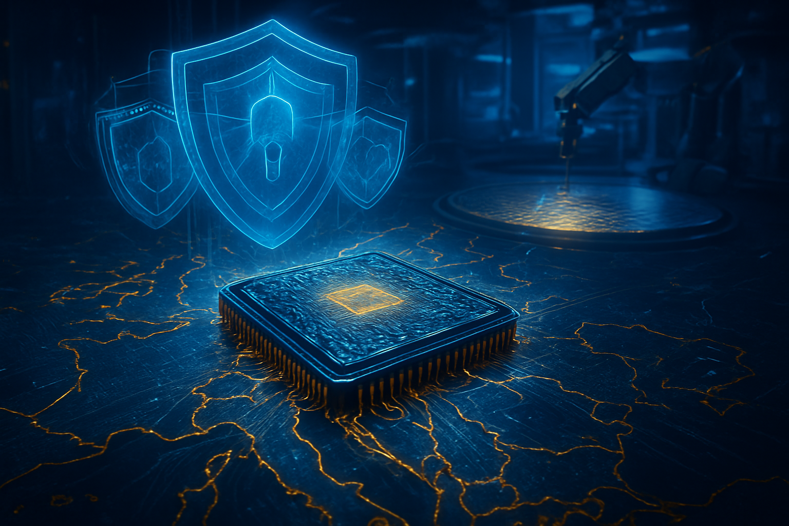
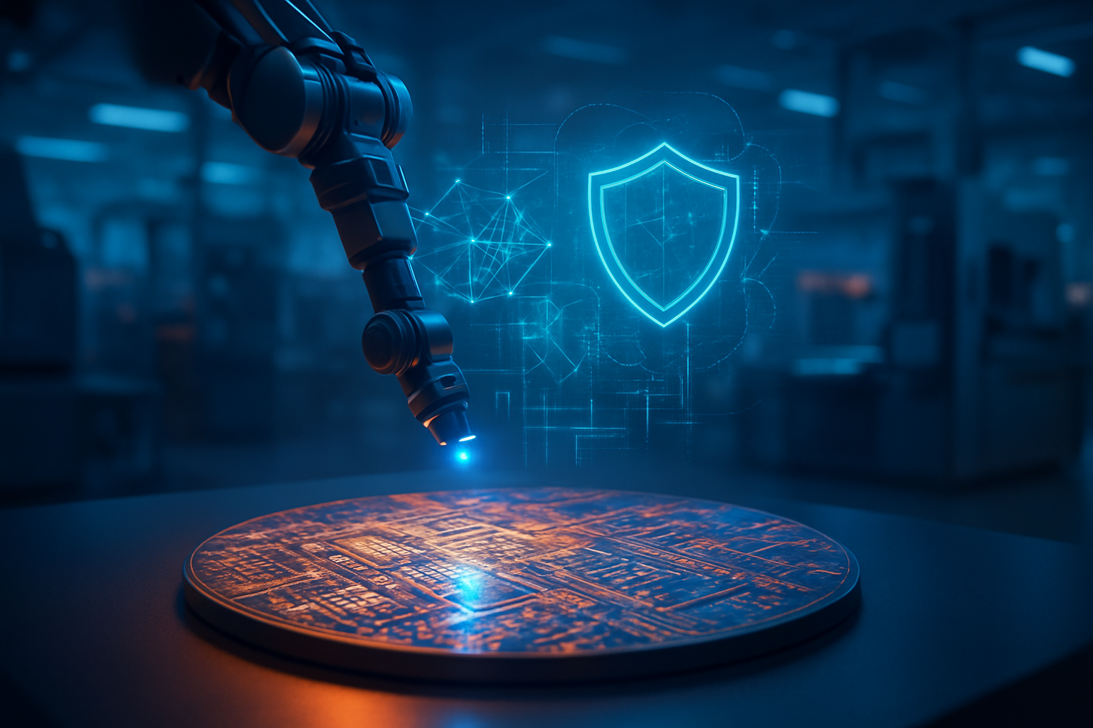
    Amkor Technology, on the other hand, is the unsung hero of the AI hardware revolution, specializing in advanced packaging solutions that are indispensable for unlocking the full potential of modern AI chips. As traditional silicon scaling (Moore's Law) faces physical limits, heterogeneous integration—combining multiple dies into a single package—has become paramount. Amkor's expertise in 2.5D Through Silicon Via (TSV) interposers, Chip on Substrate (CoS), and Chip on Wafer (CoW) technologies allows for the high-bandwidth, low-latency interconnection of high-performance logic with high-bandwidth memory (HBM), which is crucial for AI and High-Performance Computing (HPC). Their innovative S-SWIFT (Silicon Wafer Integrated Fan-Out) technology offers a cost-effective alternative to 2.5D TSV, boosting I/O and circuit density while reducing package size and improving electrical performance, making it ideal for AI applications demanding significant memory and compute power. Amkor's impressive track record, including shipping over two million 2.5D TSV products and over 2 billion eWLB (embedded Wafer Level Ball Grid Array) components, underscores its maturity and capability in powering AI and HPC applications.

    Initial reactions from the AI research community and industry experts have been overwhelmingly positive for both companies. NXP's edge AI solutions are lauded for being "cost-effective, low-power solutions for vision processing and sensor fusion," empowering efficient and private machine learning at the edge. The Kinara acquisition is seen as a move that will "enhance and strengthen NXP's ability to provide complete and scalable AI platforms, from TinyML to generative AI." For Amkor, its advanced packaging capabilities are considered critical for the future of AI. NVIDIA (NASDAQ: NVDA) CEO Jensen Huang highlighted Amkor's $7 billion Arizona campus expansion as a "defining milestone" for U.S. leadership in the "AI century." Experts recognize Fan-Out Wafer Level Packaging (FOWLP) as a key enabler for heterogeneous integration, offering superior electrical performance and thermal dissipation, central to achieving performance gains beyond traditional transistor scaling. While NXP's Q3 2025 earnings saw some mixed market reaction due to revenue decline, analysts remain bullish on its long-term prospects in automotive and industrial AI. Investors are also closely monitoring Amkor's execution and ability to manage competition amidst its significant expansion.

    Reshaping the AI Ecosystem: From Hyperscalers to the Edge

    The robust investment in AI-driven semiconductor companies like NXP and Amkor is not merely a financial phenomenon; it is fundamentally reshaping the competitive landscape for AI companies, tech giants, and startups alike. As the global AI chip market barrels towards a projected $150 billion in 2025, access to advanced, specialized hardware is becoming the ultimate differentiator, driving both unprecedented opportunities and intense competitive pressures.

    Major tech giants, including Google (NASDAQ: GOOGL), Amazon (NASDAQ: AMZN), Microsoft (NASDAQ: MSFT), and Apple (NASDAQ: AAPL), are deeply entrenched in this race, often pursuing vertical integration by designing their own custom AI accelerators—such as Google's TPUs or Microsoft's Maia and Cobalt chips. This strategy aims to optimize performance for their unique AI workloads, reduce reliance on external suppliers like NVIDIA (NASDAQ: NVDA), and gain greater strategic control over their AI infrastructure. Their vast financial resources allow them to secure long-term contracts with leading foundries like TSMC (NYSE: TSM) and benefit from the explosive growth experienced by equipment suppliers like ASML (NASDAQ: ASML). This trend creates a dual dynamic: while it fuels demand for advanced manufacturing and packaging services from companies like Amkor, it also intensifies the competition for chip design talent and foundry capacity.

    For AI companies and startups, the proliferation of advanced AI semiconductors presents both a boon and a challenge. On one hand, the availability of more powerful, energy-efficient, and specialized chips—from NXP's edge NPUs to NVIDIA's data center GPUs—accelerates innovation and deployment across various sectors, enabling the training of larger models and the execution of more complex inference tasks. This democratizes access to AI capabilities to some extent, particularly with the rise of cloud-based design tools. However, the high costs associated with these cutting-edge chips and the intense demand from hyperscalers can create significant barriers for smaller players, potentially exacerbating an "AI divide" where only well-funded entities can fully leverage the latest hardware. Companies like NXP, with their focus on accessible edge AI solutions and comprehensive software stacks, offer a pathway for startups to embed sophisticated AI into their products without requiring massive data center investments.

    The market positioning and strategic advantages are increasingly defined by specialized expertise and ecosystem control. Companies like Amkor, with its leadership in advanced packaging technologies like 2.5D TSV and S-SWIFT, wield significant pricing power and importance as they solve the critical integration challenges for heterogeneous AI chips. NXP's strategic advantage lies in its deep penetration of the automotive and industrial IoT sectors, where its secure edge processing solutions and AI-optimized microcontrollers are becoming indispensable for real-time, low-power AI applications. The acquisition of Kinara, an edge AI chipmaker, further solidifies NXP's ability to provide complete and scalable AI platforms from TinyML to generative AI at the edge. This era also highlights the critical importance of robust software ecosystems, exemplified by NVIDIA's CUDA, which creates a powerful lock-in effect, tying developers and their applications to specific hardware platforms. The overall impact is a rapid evolution of products and services, with AI-enabled PCs projected to account for 43% of all PC shipments by the end of 2025, and new computing paradigms like neuromorphic and in-memory computing gaining traction, signaling a profound disruption to traditional computing architectures and an urgent imperative for continuous innovation.

    The Broader Canvas: AI Chips as the Bedrock of a New Era

    The escalating investment in AI-driven semiconductor companies transcends mere financial trends; it represents a foundational shift in the broader AI landscape, signaling a new era where hardware innovation is as critical as algorithmic breakthroughs. This intense focus on specialized chips, advanced packaging, and edge processing capabilities is not just enabling more powerful AI, but also reshaping global economies, igniting geopolitical competition, and presenting both immense opportunities and significant concerns.

    This current AI boom is distinguished by its sheer scale and speed of adoption, marking a departure from previous AI milestones that often centered more on software advancements. Today, AI's progress is deeply and symbiotically intertwined with hardware innovation, making the semiconductor industry the bedrock of this revolution. The demand for increasingly powerful, energy-efficient, and specialized chips—from NXP's DNPUs enabling generative AI at the edge to NVIDIA's cutting-edge Blackwell and Rubin architectures powering data centers—is driving relentless innovation in chip architecture, including the exploration of neuromorphic computing, quantum computing, and advanced 3D chip stacking. This technological leap is crucial for realizing the full potential of AI, enabling applications that were once confined to science fiction across healthcare, autonomous systems, finance, and manufacturing.

    However, this rapid expansion is not without its challenges and concerns. Economically, there are growing fears of an "AI bubble," with some analysts questioning whether the massive capital expenditure on AI infrastructure, such as Microsoft's planned $80 billion investment in AI data centers, is outpacing actual economic benefits. Reports of generative AI pilot programs failing to yield significant revenue returns in businesses add to this apprehension. The market also exhibits a high concentration of value among a few top players like NVIDIA (NASDAQ: NVDA) and TSMC (NYSE: TSM), raising questions about long-term market sustainability and potential vulnerabilities if the AI momentum falters. Environmentally, the resource-intensive nature of semiconductor manufacturing and the vast energy consumption of AI data centers pose significant challenges, necessitating a concerted effort towards energy-efficient designs and sustainable practices.

    Geopolitically, AI chips have become a central battleground, particularly between the United States and China. Considered dual-use technology with both commercial and strategic military applications, AI chips are now a focal point of competition, leading to the emergence of a "Silicon Curtain." The U.S. has imposed export controls on high-end chips and advanced manufacturing equipment to China, aiming to constrain its ability to develop cutting-edge AI. In response, China is pouring billions into domestic semiconductor development, including a recent $47 billion fund for AI-grade semiconductors, in a bid for self-sufficiency. This intense competition is characterized by "semiconductor rows" and massive national investment strategies, such as the U.S. CHIPS Act ($280 billion) and the EU Chips Act (€43 billion), aimed at localizing semiconductor production and diversifying supply chains. Control over advanced semiconductors has become a critical geopolitical issue, influencing alliances, trade policies, and national security, defining 21st-century power dynamics much like oil defined the 20th century. This global scramble, while fostering resilience, may also lead to a more fragmented and costly global supply chain.

    The Road Ahead: Specialized Silicon and Pervasive AI at the Edge

    The trajectory of AI-driven semiconductors points towards an era of increasing specialization, energy efficiency, and deep integration, fundamentally reshaping how AI is developed and deployed. Both in the near-term and over the coming decades, the evolution of hardware will be the defining factor in unlocking the next generation of AI capabilities, from massive cloud-based models to pervasive intelligence at the edge.

    In the near term (1-5 years), the industry will witness accelerated adoption of advanced process nodes like 3nm and 2nm, leveraging Gate-All-Around (GAA) transistors and High-Numerical Aperture Extreme Ultraviolet (High-NA EUV) lithography for enhanced performance and reduced power consumption. The proliferation of specialized AI accelerators—beyond traditional GPUs—will continue, with Neural Processing Units (NPUs) becoming standard in mobile and edge devices, and Application-Specific Integrated Circuits (ASICs) and Field-Programmable Gate Arrays (FPGAs) offering tailored designs for specific AI computations. Heterogeneous integration and advanced packaging, a domain where Amkor Technology (NASDAQ: AMKR) excels, will become even more critical, with 3D chip stacking and chiplet architectures enabling vertical stacking of memory (e.g., HBM) and processing units to minimize data movement and boost bandwidth. Furthermore, the urgent need for energy efficiency will drive innovations like compute-in-memory and neuromorphic computing, mimicking biological neural networks for ultra-low power, real-time processing, as seen in NXP's (NASDAQ: NXPI) edge AI focus.

    Looking further ahead (beyond 5 years), the vision includes even more advanced lithography, fully modular semiconductor designs with custom chiplets, and the integration of optical interconnects within packages for ultra-high bandwidth communication. The exploration of new materials beyond silicon, such as Gallium Nitride (GaN) and Silicon Carbide (SiC), will become more prominent. Crucially, the long-term future anticipates a convergence of quantum computing and AI, or "Quantum AI," where quantum systems will act as specialized accelerators in cloud environments for tasks like drug discovery and molecular simulation. Experts also predict the emergence of biohybrid systems, integrating living neuronal cultures with synthetic neural networks for biologically realistic AI models. These advancements will unlock a plethora of applications, from powering colossal LLMs and generative AI in hyperscale cloud data centers to enabling real-time, low-power processing directly on devices like autonomous vehicles, robotics, and smart IoT sensors, fundamentally transforming industries and enhancing data privacy by keeping AI processing local.

    However, this ambitious trajectory is fraught with significant challenges. Technically, the industry must overcome the immense power consumption and heat dissipation of AI workloads, the escalating manufacturing complexity at atomic scales, and the physical limits of traditional silicon scaling. Economically, the astronomical costs of building modern fabrication plants (fabs) and R&D, coupled with a current funding gap in AI infrastructure compared to foundation models, pose substantial hurdles. Geopolitical risks, stemming from concentrated global supply chains and trade tensions, threaten stability, while environmental and ethical concerns—including the vast energy consumption, carbon footprint, algorithmic bias, and potential misuse of AI—demand urgent attention. Experts predict that the next phase of AI will be defined by hardware's ability to bring intelligence into physical systems with precision and durability, making silicon almost as "codable" as software. This continuous wave of innovation in specialized, energy-efficient chips is expected to drive down costs and democratize access to powerful generative AI, leading to a ubiquitous presence of edge AI across all sectors and a more competitive landscape challenging the current dominance of a few key players.

    A New Industrial Revolution: The Enduring Significance of AI's Silicon Foundation

    The unprecedented surge in investment in AI-driven semiconductor companies marks a pivotal, transformative moment in AI history, akin to a new industrial revolution. This robust capital inflow, driven by the insatiable demand for advanced computing power, is not merely a fleeting trend but a foundational shift that is profoundly reshaping global technological landscapes and supply chains. The performance of companies like NXP Semiconductors (NASDAQ: NXPI) and Amkor Technology (NASDAQ: AMKR) serves as a potent barometer of this underlying re-architecture of the digital world.

    The key takeaway from this investment wave is the undeniable reality that semiconductors are no longer just components; they are the indispensable bedrock underpinning all advanced computing, especially AI. This era is defined by an "AI Supercycle," where the escalating demand for computational power fuels continuous chip innovation, which in turn unlocks even more sophisticated AI capabilities. This symbiotic relationship extends beyond merely utilizing chips, as AI is now actively involved in the very design and manufacturing of its own hardware, significantly shortening design cycles and enhancing efficiency. This deep integration signifies AI's evolution from a mere application to becoming an integral part of computing infrastructure itself. Moreover, the intense focus on chip resilience and control has elevated semiconductor manufacturing to a critical strategic domain, intrinsically linked to national security, economic growth, and geopolitical influence, as nations race to establish technological sovereignty.

    Looking ahead, the long-term impact of these investment trends points towards a future of continuous technological acceleration across virtually all sectors, powered by advanced edge AI, neuromorphic computing, and eventually, quantum computing. Breakthroughs in novel computing paradigms and the continued reshaping of global supply chains towards more regionalized and resilient models are anticipated. While this may entail higher costs in the short term, it aims to enhance long-term stability. Increased competition from both established rivals and emerging AI chip startups is expected to intensify, challenging the dominance of current market leaders. However, the immense energy consumption associated with AI and chip production necessitates sustained investment in sustainable solutions, and persistent talent shortages in the semiconductor industry will remain a critical hurdle. Despite some concerns about a potential "AI bubble," the prevailing sentiment is that current AI investments are backed by cash-rich companies with strong business models, laying a solid foundation for future growth.

    In the coming weeks and months, several key developments warrant close attention. The commencement of high-volume manufacturing for 2nm chips, expected in late 2025 with significant commercial adoption by 2026-2027, will be a critical indicator of technological advancement. The continued expansion of advanced packaging and heterogeneous integration techniques, such as 3D chip stacking, will be crucial for boosting chip density and reducing latency. For Amkor Technology, the progress on its $7 billion advanced packaging and test campus in Arizona, with production slated for early 2028, will be a major focal point, as it aims to establish a critical "end-to-end silicon supply chain in America." NXP Semiconductors' strategic collaborations, such as integrating NVIDIA's TAO Toolkit APIs into its eIQ machine learning development environment, and the successful integration of its Kinara acquisition, will demonstrate its continued leadership in secure edge processing and AI-optimized solutions for automotive and industrial sectors. Geopolitical developments, particularly changes in government policies and trade restrictions like the proposed "GAIN AI Act," will continue to influence semiconductor supply chains and investment flows. Investor confidence will also be gauged by upcoming earnings reports from major chipmakers and hyperscalers, looking for sustained AI-related spending and expanding profit margins. Finally, the tight supply conditions and rising prices for High-Bandwidth Memory (HBM) are expected to persist through 2027, making this a key area to watch in the memory chip market. The "AI Supercycle" is just beginning, and the silicon beneath it is more critical than ever.


    This content is intended for informational purposes only and represents analysis of current AI developments.

    TokenRing AI delivers enterprise-grade solutions for multi-agent AI workflow orchestration, AI-powered development tools, and seamless remote collaboration platforms.
    For more information, visit https://www.tokenring.ai/.

  • NXP and eInfochips Forge Alliance to Power Software-Defined Vehicle Revolution

    NXP and eInfochips Forge Alliance to Power Software-Defined Vehicle Revolution

    Eindhoven, Netherlands & San Jose, CA – October 24, 2025 – In a strategic move set to significantly accelerate the development and deployment of software-defined vehicles (SDVs), NXP Semiconductors (NASDAQ: NXPI) has announced a multi-year partnership with eInfochips, an Arrow Electronics company. This collaboration, officially unveiled on October 23, 2025, is designed to revolutionize software distribution and elevate customer support for NXP's critical S32 platform, a cornerstone of the automotive industry's shift towards intelligent, connected, and autonomous vehicles. The alliance is poised to streamline the complex process of integrating advanced automotive software, promising faster innovation cycles and more robust solutions for manufacturers worldwide.

    This partnership comes at a pivotal time when the automotive sector is undergoing a profound transformation, driven by the increasing complexity of vehicle software. By leveraging eInfochips' extensive engineering expertise and NXP's cutting-edge S32 processors, the initiative aims to simplify access to essential software packages and provide unparalleled technical assistance, thereby empowering developers and accelerating the journey towards a fully software-defined automotive future.

    Technical Deep Dive: Enhancing the S32 Ecosystem for SDVs

    The core of this transformative partnership lies in bolstering the NXP S32 family of microcontrollers and microprocessors, which are central to modern automotive architectures. eInfochips, already recognized as an NXP Gold Partner, will now play a pivotal role in distributing standard and premium software packages and tools specifically tailored for the S32 platform. This includes critical components for connected car solutions, hardware acceleration, telemetry applications, and Fast Path Packet Forwarding on S32-based reference designs. The S32 platform, particularly with the integration of S32 CoreRide, is NXP's strategic answer to the demands of software-defined vehicles, providing a robust foundation for hardware-software integration and reference designs.

    This collaboration marks a significant departure from traditional software support models. By entrusting eInfochips with comprehensive software support and maintenance, NXP is creating a more agile and responsive ecosystem. This "best-in-class support" system is engineered to facilitate successful and efficient application development, dramatically reducing time-to-market for customers. Unlike previous approaches that might have involved more fragmented support channels, this consolidated effort ensures that NXP customers integrating S32 processors and microcontrollers receive consistent, high-quality technical and functional safety support, including ongoing assistance for battery energy storage systems. Initial reactions from the automotive embedded software community highlight the potential for this partnership to standardize and simplify development workflows, which has long been a challenge in the highly complex automotive domain.

    Competitive Implications and Market Positioning

    This strategic alliance carries significant implications for AI companies, tech giants, and startups operating within the automotive and embedded systems space. NXP Semiconductors (NASDAQ: NXPI) stands to significantly benefit by strengthening its position as a leading provider of automotive semiconductor solutions. By enhancing its software ecosystem and support services through eInfochips, NXP makes its S32 platform even more attractive to automotive OEMs and Tier 1 suppliers, who are increasingly prioritizing comprehensive software enablement. This move directly addresses a critical pain point in the industry: the complexity of integrating and maintaining software on high-performance automotive hardware.

    For tech giants and major AI labs venturing into automotive software, this partnership provides a more robust and supported platform for their innovations. Companies developing advanced driver-assistance systems (ADAS), infotainment systems, and autonomous driving algorithms will find a more streamlined path to deployment on NXP's S32 platform. Conversely, this development could intensify competitive pressures on other semiconductor manufacturers who may not offer as integrated or well-supported a software ecosystem. Startups specializing in automotive software development tools, middleware, or specific application development for SDVs might find new opportunities to collaborate within this expanded NXP-eInfochips ecosystem, potentially becoming solution partners or benefiting from improved platform stability. The partnership solidifies NXP's market positioning by offering a compelling, end-to-end solution that spans hardware, software, and critical support, thereby creating a strategic advantage in the rapidly evolving SDV landscape.

    Wider Significance in the AI and Automotive Landscape

    This partnership is a clear indicator of the broader trend towards software-defined everything, a paradigm shift that is profoundly impacting the AI and automotive industries. As vehicles become sophisticated rolling computers, the software stack becomes as critical, if not more so, than the hardware. This collaboration fits perfectly into the evolving AI landscape by providing a more accessible and supported platform for deploying AI-powered features, from advanced perception systems to predictive maintenance and personalized user experiences. The emphasis on streamlining software distribution and support directly addresses the challenges of managing complex AI models and algorithms in safety-critical automotive environments.

    The impacts are far-reaching. It promises to accelerate the adoption of advanced AI features in production vehicles by reducing development friction. Potential concerns, however, could revolve around the consolidation of software support, though NXP and eInfochips aim to deliver best-in-class service. This development can be compared to previous AI milestones where foundational platforms or ecosystems were significantly enhanced, such as the maturation of cloud AI platforms or specialized AI development kits. By making the underlying automotive computing platform more developer-friendly, NXP and eInfochips are effectively lowering the barrier to entry for AI innovation in vehicles, potentially leading to a faster pace of innovation and differentiation in the market. It underscores the critical importance of a robust software ecosystem for hardware providers in the age of AI.

    Future Developments and Expert Predictions

    Looking ahead, this partnership is expected to yield several near-term and long-term developments. In the near term, customers can anticipate a more seamless experience in acquiring and integrating NXP S32 software, coupled with enhanced, responsive technical support. This will likely translate into faster project timelines and reduced development costs for automotive OEMs and Tier 1 suppliers. Long-term, the collaboration is poised to foster an even richer ecosystem around the S32 CoreRide platform, potentially leading to the co-development of new software tools, specialized modules, and advanced reference designs optimized for AI and autonomous driving applications. We can expect to see more integrated solutions that combine NXP's hardware capabilities with eInfochips' software expertise, pushing the boundaries of what's possible in SDVs.

    Potential applications and use cases on the horizon include highly sophisticated AI inference at the edge within vehicles, advanced sensor fusion algorithms, and over-the-air (OTA) update capabilities that are more robust and secure. Challenges that need to be addressed include continuously scaling the support infrastructure to meet growing demands, ensuring seamless integration with diverse customer development environments, and staying ahead of rapidly evolving automotive software standards and cybersecurity threats. Experts predict that this kind of deep hardware-software partnership will become increasingly common as the industry moves towards greater software definition, ultimately leading to more innovative, safer, and more personalized driving experiences. The focus will shift even more towards integrated solutions rather than disparate components.

    A New Era for Automotive Software Ecosystems

    The partnership between NXP Semiconductors and eInfochips represents a significant milestone in the evolution of automotive software ecosystems. The key takeaway is the strategic emphasis on streamlining software distribution and providing comprehensive customer support for NXP's critical S32 platform, directly addressing the complexities inherent in developing software-defined vehicles. This collaboration is set to empower automotive manufacturers and developers, accelerating their journey towards bringing next-generation AI-powered vehicles to market.

    In the grand tapestry of AI history, this development underscores the growing importance of robust, integrated platforms that bridge the gap between advanced hardware and sophisticated software. It highlights that even the most powerful AI chips require a well-supported and accessible software ecosystem to unlock their full potential. The long-term impact will likely be a more efficient, innovative, and competitive automotive industry, where software differentiation becomes a primary driver of value. In the coming weeks and months, industry observers will be watching closely for initial customer feedback, the rollout of new software packages, and how this partnership further solidifies NXP's leadership in the software-defined vehicle space.


    This content is intended for informational purposes only and represents analysis of current AI developments.

    TokenRing AI delivers enterprise-grade solutions for multi-agent AI workflow orchestration, AI-powered development tools, and seamless remote collaboration platforms.
    For more information, visit https://www.tokenring.ai/.

  • The AI Supercycle: Semiconductors Powering the Future, Navigating Challenges and Unprecedented Opportunities

    The AI Supercycle: Semiconductors Powering the Future, Navigating Challenges and Unprecedented Opportunities

    The global semiconductor market is in the throes of an unprecedented "AI Supercycle," a period of explosive growth and transformative innovation driven by the insatiable demand for Artificial Intelligence capabilities. As of October 3, 2025, this synergy between AI and silicon is not merely enhancing existing technologies but fundamentally redefining the industry's landscape, pushing the boundaries of innovation, and creating both immense opportunities and significant challenges for the tech world and beyond. The foundational hardware that underpins every AI advancement, from complex machine learning models to real-time edge applications, is seeing unparalleled investment and strategic importance, with the market projected to reach approximately $800 billion in 2025 and set to surpass $1 trillion by 2030.

    This surge is not just a passing trend; it is a structural shift. AI chips alone are projected to generate over $150 billion in sales in 2025, constituting more than 20% of total chip sales. This growth is primarily fueled by generative AI, high-performance computing (HPC), and the proliferation of AI at the edge, impacting everything from data centers to autonomous vehicles and consumer electronics. The semiconductor industry's ability to innovate and scale will be the ultimate determinant of AI's future trajectory, making it the most critical enabling technology of our digital age.

    The Silicon Engine of Intelligence: Detailed Market Dynamics

    The current semiconductor market is characterized by a relentless drive for specialization, efficiency, and advanced integration, directly addressing the escalating computational demands of AI. This era is witnessing a profound shift from general-purpose processing to highly optimized silicon solutions.

    Specialized AI chips, including Graphics Processing Units (GPUs), Application-Specific Integrated Circuits (ASICs), Tensor Processing Units (TPUs), and Neural Processing Units (NPUs), are experiencing skyrocketing demand. These components are meticulously designed for optimal performance in AI workloads such as deep learning, natural language processing, and computer vision. Companies like NVIDIA (NASDAQ: NVDA) continue to dominate the high-end GPU market, while others like Broadcom (NASDAQ: AVGO) and Marvell (NASDAQ: MRVL) are making significant strides in custom AI ASICs, reflecting a broader trend of tech giants developing their own in-house silicon to tailor chips specifically for their AI workloads.

    With the traditional scaling limits of Moore's Law becoming more challenging, innovations in advanced packaging are taking center stage. Technologies like 2.5D/3D integration, hybrid bonding, and chiplets are crucial for increasing chip density, reducing latency, and improving power consumption. High-Bandwidth Memory (HBM) is also seeing a substantial surge, with its market revenue expected to hit $21 billion in 2025, a 70% year-over-year increase, as it becomes indispensable for AI accelerators. This push for heterogeneous computing, combining different processor types in a single system, is optimizing performance for diverse AI workloads. Furthermore, AI is not merely a consumer of semiconductors; it is also a powerful tool revolutionizing their design, manufacturing, and supply chain management, enhancing R&D efficiency, optimizing production, and improving yield.

    However, this rapid advancement is not without its hurdles. The computational complexity and power consumption of AI algorithms pose significant challenges. AI workloads generate immense heat, necessitating advanced cooling solutions, and large-scale AI models consume vast amounts of electricity. The rising costs of innovation, particularly for advanced process nodes (e.g., 3nm, 2nm), place a steep price tag on R&D and fabrication. Geopolitical tensions, especially between the U.S. and China, continue to reshape the industry through export controls and efforts for regional self-sufficiency, leading to supply chain vulnerabilities. Memory bandwidth remains a critical bottleneck for AI models requiring fast access to large datasets, and a global talent shortage persists, particularly for skilled AI and semiconductor manufacturing experts.

    NXP and SOXX Reflecting the AI-Driven Market: Company Performances and Competitive Landscape

    The performances of key industry players and indices vividly illustrate the impact of the AI Supercycle on the semiconductor market. NXP Semiconductors (NASDAQ: NXPI) and the iShares Semiconductor ETF (SOXX) serve as compelling barometers of this dynamic environment as of October 3, 2025.

    NXP Semiconductors, a dominant force in the automotive and industrial & IoT sectors, reported robust financial results for Q2 2025, with $2.93 billion in revenue, exceeding market forecasts. While experiencing some year-over-year decline, the company's optimistic Q3 2025 guidance, projecting revenue between $3.05 billion and $3.25 billion, signals an "emerging cyclical improvement" in its core end markets. NXP's strategic moves underscore its commitment to the AI-driven future: the acquisition of TTTech Auto in June 2025 enhances its capabilities in safety-critical systems for software-defined vehicles (SDVs), and the acquisition of AI processor company Kinara.ai in February 2025 further bolsters its AI portfolio. The unveiling of its third-generation S32R47 imaging radar processors for autonomous driving also highlights its deep integration into AI-enabled automotive solutions. NXP's stock performance reflects this strategic positioning, showing impressive long-term gains despite some recent choppiness, with analysts maintaining a "Moderate Buy" consensus.

    The iShares Semiconductor ETF (SOXX), which tracks the NYSE Semiconductor Index, has demonstrated exceptional performance, with a Year-to-Date total return of 28.97% as of October 1, 2025. The underlying Philadelphia Semiconductor Index (SOX) also reflects significant growth, having risen 31.69% over the past year. This robust performance is a direct consequence of the "insatiable hunger" for computational power driven by AI. The ETF's holdings, comprising major players in high-performance computing and specialized chip development like NVIDIA (NASDAQ: NVDA), Broadcom (NASDAQ: AVGO), and TSMC (NYSE: TSM), directly benefit from the surge in AI-driven demand across data centers, automotive, and other applications.

    For AI companies, these trends have profound competitive implications. Companies developing AI models and applications are critically dependent on these hardware advancements to achieve greater computational power, reduce latency, and enable more sophisticated features. The semiconductor industry's ability to produce next-generation processors and components like HBM directly fuels the capabilities of AI, making the semiconductor sector the foundational backbone for the future trajectory of AI development. While NVIDIA currently holds a dominant market share in AI ICs, the rise of custom silicon from tech giants and the emergence of new players focusing on inference-optimized solutions are fostering a more competitive landscape, potentially disrupting existing product ecosystems and creating new strategic advantages for those who can innovate in both hardware and software.

    The Broader AI Landscape: Wider Significance and Impacts

    The current semiconductor market trends are not just about faster chips; they represent a fundamental reshaping of the broader AI landscape, impacting its trajectory, capabilities, and societal implications. This period, as of October 2025, marks a distinct phase in AI's evolution, characterized by an unprecedented hardware-software co-evolution.

    The availability of powerful, specialized chips is directly accelerating the development of advanced AI, including larger and more capable large language models (LLMs) and autonomous agents. This computational infrastructure is enabling breakthroughs in areas that were previously considered intractable. We are also witnessing a significant shift towards inference dominance, where real-time AI applications drive the need for specialized hardware optimized for inference tasks, moving beyond the intensive training phase. This enables AI to be deployed in a myriad of real-world scenarios, from intelligent assistants to predictive maintenance.

    However, this rapid advancement comes with significant concerns. The explosive growth of AI applications, particularly in data centers, is leading to surging power consumption. AI servers demand substantially more power than general servers, with data center electricity demand projected to reach 11-12% of the United States' total by 2030. This places immense strain on energy grids and raises environmental concerns, necessitating huge investments in renewable energy and innovative energy-efficient hardware. Furthermore, the AI chip industry faces rising risks from raw material shortages, geopolitical conflicts, and a heavy dependence on a few key manufacturers, primarily in Taiwan and South Korea, creating vulnerabilities in the global supply chain. The astronomical cost of developing and manufacturing advanced AI chips also creates a massive barrier to entry for startups and smaller companies, potentially centralizing AI power in the hands of a few tech giants.

    Comparing this era to previous AI milestones reveals a profound evolution. In the early days of AI and machine learning, hardware was less specialized, relying on general-purpose CPUs. The deep learning revolution of the 2010s was ignited by the realization that GPUs, initially for gaming, were highly effective for neural network training, making hardware a key accelerator. The current era, however, is defined by "extreme specialization" with ASICs, NPUs, and TPUs explicitly designed for AI workloads. Moreover, as traditional transistor scaling slows, innovations in advanced packaging are critical for continued performance gains, effectively creating "systems of chips" rather than relying solely on monolithic integration. Crucially, AI is now actively used within the semiconductor design and manufacturing process itself, creating a powerful feedback loop of innovation. This intertwining of AI and semiconductors has elevated the latter to a critical strategic asset, deeply entwined with national security and technological sovereignty, a dimension far more pronounced than in any previous AI milestone.

    The Horizon of Innovation: Exploring Future Developments

    Looking ahead, the semiconductor market is poised for continued transformative growth, driven by the escalating demands of AI. Near-term (2025-2030) and long-term (beyond 2030) developments promise to unlock unprecedented AI capabilities, though significant challenges remain.

    In the near-term, the relentless pursuit of miniaturization will continue with advancements in 3nm and 2nm manufacturing nodes, crucial for enhancing AI's potential across industries. The focus on specialized AI processors will intensify, with custom ASICs and NPUs becoming more prevalent for both data centers and edge devices. Tech giants will continue investing heavily in proprietary chips to optimize for their specific cloud infrastructures and inference workloads, while companies like Broadcom (NASDAQ: AVGO) will remain key players in AI ASIC development. Advanced packaging technologies, such as 2.5D and 3D stacking, will become even more critical, integrating multiple components to boost performance and reduce power consumption. High-Bandwidth Memory (HBM4 and HBM4E) is expected to see widespread adoption to keep pace with AI's computational requirements. The proliferation of Edge AI and on-device AI will continue, with semiconductor manufacturers developing chips optimized for local data processing, reducing latency, conserving bandwidth, and enhancing privacy for real-time applications. The escalating energy requirements of AI will also drive intense efforts to develop low-power technologies and more energy-efficient inference chips, with startups challenging established players through innovative designs.

    Beyond 2030, the long-term vision includes the commercialization of neuromorphic computing, a brain-inspired AI paradigm offering ultra-low power consumption and real-time processing for edge AI, cybersecurity, and autonomous systems. While quantum computing is still 10-15 years away from replacing generative AI workloads, it is expected to complement and amplify AI for complex simulation tasks in drug discovery and advanced materials design. Innovations in new materials and architectures, including silicon photonics for light-based data transmission, will continue to drive radical shifts in AI processing. Experts predict the global semiconductor market to surpass $1 trillion by 2030 and potentially $2 trillion by 2040, primarily fueled by the "AI supercycle." AI itself is expected to lead to the total automation of semiconductor design, with AI-driven tools creating chip architectures and enhancing performance without human assistance, generating significant value in manufacturing.

    However, several challenges need addressing. AI's power consumption is quickly becoming one of the most daunting challenges, with energy generation potentially becoming the most significant constraint on future AI expansion. The astronomical cost of building advanced fabrication plants and the increasing technological complexity of chip designs pose significant hurdles. Geopolitical risks, talent shortages, and the need for standardization in emerging fields like neuromorphic computing also require concerted effort from industry, academia, and governments.

    The Foundation of Tomorrow: A Comprehensive Wrap-up

    The semiconductor market, as of October 2025, stands as the undisputed bedrock of the AI revolution. The "AI Supercycle" is driving unprecedented demand, innovation, and strategic importance for silicon, fundamentally shaping the trajectory of artificial intelligence. Key takeaways include the relentless drive towards specialized AI chips, the critical role of advanced packaging in overcoming Moore's Law limitations, and the profound impact of AI on both data centers and the burgeoning edge computing landscape.

    This period represents a pivotal moment in AI history, distinguishing itself from previous milestones through extreme specialization, the centrality of semiconductors in geopolitical strategies, and the emergent challenge of AI's energy consumption. The robust performance of companies like NXP Semiconductors (NASDAQ: NXPI) and the iShares Semiconductor ETF (SOXX) underscores the industry's resilience and its ability to capitalize on AI-driven demand, even amidst broader economic fluctuations. These performances are not just financial indicators but reflections of the foundational advancements that empower every AI breakthrough.

    Looking ahead, the symbiotic relationship between AI and semiconductors will only deepen. The continuous pursuit of smaller, more efficient, and more specialized chips, coupled with the exploration of novel computing paradigms like neuromorphic and quantum computing, promises to unlock AI capabilities that are currently unimaginable. However, addressing the escalating power consumption, managing supply chain vulnerabilities, and fostering a skilled talent pool will be paramount to sustaining this growth.

    In the coming weeks and months, industry watchers should closely monitor advancements in 2nm and 1.4nm process nodes, further strategic acquisitions and partnerships in the AI chip space, and the rollout of more energy-efficient inference solutions. The interplay between geopolitical decisions and semiconductor manufacturing will also remain a critical factor. Ultimately, the future of AI is inextricably linked to the future of semiconductors, making this market not just a subject of business news, but a vital indicator of humanity's technological progress.

    This content is intended for informational purposes only and represents analysis of current AI developments.

    TokenRing AI delivers enterprise-grade solutions for multi-agent AI workflow orchestration, AI-powered development tools, and seamless remote collaboration platforms.
    For more information, visit https://www.tokenring.ai/.