Tag: Panther Lake

  • Intel’s 18A Era: Reclaiming Silicon Supremacy as Panther Lake Enters High-Volume Manufacturing

    Intel’s 18A Era: Reclaiming Silicon Supremacy as Panther Lake Enters High-Volume Manufacturing

    In a move that signals a seismic shift in the semiconductor industry, Intel (NASDAQ: INTC) has officially transitioned its 18A process node into high-volume manufacturing (HVM) as of January 2026. This milestone marks the culmination of the company’s ambitious "five nodes in four years" strategy, positioning Intel at the vanguard of the 2nm-class era. The launch of the Core Ultra Series 3, codenamed "Panther Lake," serves as the commercial vanguard for this transition, promising a radical leap in AI processing power and energy efficiency that challenges the recent dominance of rival foundry players and chip designers alike.

    The arrival of 18A is not merely a technical upgrade; it is a strategic reclamation of process leadership for the American chipmaker. By achieving HVM status at its Fab 52 facility in Arizona, Intel has effectively shortened the gap with TSMC (NYSE: TSM), delivering the world’s first high-volume chips featuring both Gate-All-Around (GAA) transistors and backside power delivery. As the industry pivot toward the "AI PC" accelerates, Intel’s 18A node provides the hardware foundation for the next generation of local generative AI, enabling massive computational throughput at the edge while simultaneously courting high-profile foundry customers like Microsoft (NASDAQ: MSFT) and Amazon (NASDAQ: AMZN).

    RibbonFET and PowerVia: The Architecture of 2026

    The technical backbone of the 18A node lies in two foundational innovations: RibbonFET and PowerVia. RibbonFET represents Intel’s implementation of the Gate-All-Around (GAA) transistor architecture, which replaces the long-standing FinFET design. By surrounding the transistor channel with the gate on all four sides, RibbonFET provides superior electrostatic control, drastically reducing current leakage and allowing for higher drive currents at lower voltages. This is paired with PowerVia, a pioneering "backside power delivery" technology that moves power routing to the underside of the silicon wafer. This separation of power and signal lines minimizes electrical interference and reduces voltage drop (IR drop) by up to 30%, a critical factor in maintaining performance while shrinking transistor sizes.

    The first product to leverage these technologies is the Core Ultra Series 3 (Panther Lake) processor family, which hit retail shelves in late January 2026. Panther Lake utilizes a sophisticated multi-tile architecture, integrating the new "Cougar Cove" performance cores and "Darkmont" efficiency cores. Early benchmarks suggest a staggering 25% improvement in performance-per-watt compared to the previous Lunar Lake generation. Furthermore, the inclusion of the third-generation Xe3 (Battlemage) integrated graphics and a massive NPU 5 (Neural Processing Unit) capable of 50 TOPS (Tera Operations Per Second) positions Panther Lake as the premier platform for on-device AI applications, such as real-time language translation and advanced generative image editing.

    Industry reactions have been cautiously optimistic, with analysts noting that Intel has successfully navigated the yield challenges that often plague such radical architectural shifts. Initial reports indicate that 18A yields at the Arizona Fab 52 have stabilized above the 60% threshold—a commercially viable figure for a leading-edge ramp. While TSMC (NYSE: TSM) remains a formidable competitor with its N2 node, Intel’s decision to integrate backside power delivery earlier than its rivals has given it a temporary but significant "efficiency lead" in the mobile and ultra-thin laptop segments.

    The AI Arms Race: Why 18A Matters for Microsoft, Amazon, and Beyond

    Intel’s 18A node is more than just a win for its consumer processors; it is the cornerstone of its newly independent Intel Foundry business. The successful HVM of 18A has already secured "whale" customers who are desperate for advanced domestic manufacturing capacity. Microsoft (NASDAQ: MSFT) has confirmed that its next-generation Maia 3 AI accelerators will be built on the 18A and 18A-P nodes, seeking to decouple its AI infrastructure from a total reliance on Taiwanese manufacturing. Similarly, Amazon (NASDAQ: AMZN) Web Services (AWS) is partnering with Intel for a custom 18A "AI fabric" chip designed to enhance data center interconnects, signaling a shift in how hyperscalers view Intel as a manufacturing partner.

    The competitive implications for the broader AI landscape are profound. For years, NVIDIA (NASDAQ: NVDA) and AMD (NASDAQ: AMD) have relied almost exclusively on TSMC for their top-tier AI GPUs. Intel’s 18A provides a viable, high-performance alternative that could disrupt existing supply chain dynamics. If Intel can continue to scale 18A production, it may force a pricing war among foundries, ultimately benefiting AI startups and research labs by lowering the cost of advanced silicon. Furthermore, the enhanced power efficiency of 18A-based chips is a direct challenge to Apple (NASDAQ: AAPL), whose M-series chips have long set the bar for battery life in premium notebooks.

    The rise of the "AI PC" also creates a new battleground for software developers. With Panther Lake’s NPU 5, Intel is pushing a vision where AI workloads are handled locally rather than in the cloud, offering better privacy and lower latency. This move is expected to catalyze a new wave of AI-native applications from Adobe to Microsoft, specifically optimized for the 18A architecture. For the first time in a decade, Intel is not just keeping pace with the industry; it is setting the technical requirements for the next era of personal computing.

    Geopolitics and the Silicon Shield: The Rise of Fab 52

    The strategic significance of Intel 18A extends into the realm of global geopolitics. Fab 52 in Chandler, Arizona, is the first facility in the United States capable of producing 2nm-class logic chips at high volume. This achievement is a major win for the U.S. CHIPS and Science Act, which provided billions in subsidies to bring leading-edge semiconductor manufacturing back to American soil. In an era of heightened geopolitical tensions and supply chain vulnerabilities, the ability to manufacture the world’s most advanced AI chips domestically provides a "silicon shield" for the U.S. economy and national security.

    This domestic pivot also addresses growing concerns within the Department of Defense (DoD), which is utilizing the 18A node for its RAMP-C (Rapid Assured Microelectronics Prototypes – Commercial) program. By ensuring a secure, domestic supply of high-performance chips, the U.S. government is mitigating the risks associated with a potential conflict in the Taiwan Strait. Intel’s success with 18A validates the billions in taxpayer investment and cements the Arizona Ocotillo campus as one of the most technologically advanced manufacturing hubs on the planet.

    Comparatively, the 18A milestone is being viewed by historians as a potential turning point similar to Intel's shift to FinFET in 2011. While the company famously stumbled during the 10nm and 7nm transitions, the 18A era suggests that the "Intel is back" narrative is more than just marketing rhetoric. The integration of PowerVia and RibbonFET represents a "double-jump" in technology that has forced competitors to accelerate their own roadmaps. However, the pressure remains high; maintaining this lead requires Intel to flawlessly execute its next steps without the yield regressions that haunted its past.

    Beyond 18A: The Roadmap to 14A and Autonomous AI Systems

    As 18A reaches its stride, Intel is already looking toward the horizon with its 14A (1.4nm) and 10A nodes. Expected to enter risk production in late 2026 or early 2027, the 14A node will introduce High-NA (Numerical Aperture) EUV lithography, further pushing the limits of Moore's Law. These future nodes are being designed with "Autonomous AI Systems" in mind—chips that can dynamically reconfigure their internal logic gates to optimize for specific AI models, such as Large Language Models (LLMs) or complex vision transformers.

    The long-term vision for Intel Foundry is to create a seamless ecosystem where "chiplets" from different vendors can be integrated onto a single package using Intel’s advanced 3D-stacking technologies (Foveros Direct). We can expect to see future versions of the Core Ultra series featuring 18A logic paired with specialized AI accelerators from third-party partners, all manufactured under one roof in Arizona. The challenge will be the sheer complexity of these designs; as transistors shrink toward the atomic scale, the margin for error becomes nonexistent, and the cost of design and manufacturing continues to skyrocket.

    A New Chapter for the Semiconductor Industry

    The high-volume manufacturing of the Intel 18A node and the launch of Panther Lake represent a pivotal moment in the history of computing. Intel has successfully navigated a high-stakes transition, proving that it can still innovate at the bleeding edge of physics. The combination of RibbonFET and PowerVia has set a new benchmark for power efficiency and performance that will define the hardware landscape for the remainder of the decade.

    Key takeaways from this development include the successful validation of the IDM 2.0 strategy, the emergence of a viable domestic alternative to Asian foundries, and the solidifying of the "AI PC" as the primary driver of consumer hardware sales. In the coming months, the industry will be watching closely to see how TSMC responds with its N2 volume ramp and how quickly Intel can onboard additional foundry customers to its 18A ecosystem. For now, the silicon crown is back in play, and the race for AI supremacy has entered a blistering new phase.


    This content is intended for informational purposes only and represents analysis of current AI developments.

    TokenRing AI delivers enterprise-grade solutions for multi-agent AI workflow orchestration, AI-powered development tools, and seamless remote collaboration platforms.
    For more information, visit https://www.tokenring.ai/.
  • Intel’s 18A Moonshot Lands: Panther Lake Shipped, Surpassing Apple M5 by 33% in Multi-Core Dominance

    Intel’s 18A Moonshot Lands: Panther Lake Shipped, Surpassing Apple M5 by 33% in Multi-Core Dominance

    In a landmark moment for the semiconductor industry, Intel Corporation (NASDAQ: INTC) has officially begun shipping its highly anticipated Panther Lake processors, branded as Core Ultra Series 3. The launch, which took place in late January 2026, marks the successful high-volume manufacturing of the Intel 18A process node at the company’s Ocotillo campus in Arizona. For Intel, this is more than just a product release; it is the final validation of CEO Pat Gelsinger’s ambitious "5-nodes-in-4-years" turnaround strategy, positioning the company at the bleeding edge of logic manufacturing once again.

    Early third-party benchmarks and internal validation data indicate that Panther Lake has achieved a stunning 33% multi-core performance lead over the Apple Inc. (NASDAQ: AAPL) M5 processor, which launched late last year. This performance delta signals a massive shift in the mobile computing landscape, where Apple’s silicon has held the crown for efficiency and multi-threaded throughput for over half a decade. By successfully delivering 18A on schedule, Intel has not only regained parity with Taiwan Semiconductor Manufacturing Company (NYSE: TSM) but has arguably moved ahead in the integration of next-generation transistor technologies.

    Technical Mastery: RibbonFET, PowerVia, and the Xe3 Leap

    At the heart of Panther Lake’s dominance is the Intel 18A process, which introduces two revolutionary technologies to high-volume manufacturing: RibbonFET and PowerVia. RibbonFET, Intel's implementation of gate-all-around (GAA) transistors, provides superior control over the transistor channel, significantly reducing power leakage while increasing drive current. Complementing this is PowerVia, the industry's first commercial implementation of backside power delivery. By moving power routing to the rear of the silicon wafer, Intel has eliminated the "wiring congestion" that has plagued chip designers for years, allowing for higher clock speeds and improved thermal management.

    The architecture of Panther Lake itself is a hybrid marvel. It features the new "Cougar Cove" Performance-cores (P-cores) and "Darkmont" Efficient-cores (E-cores). The Darkmont cores are particularly notable; they provide such a massive leap in IPC (Instructions Per Cycle) that they reportedly rival the performance of previous-generation performance cores while consuming a fraction of the power. This architectural synergy, combined with the 18A process's density, is what allows the flagship 16-core mobile SKUs to handily outperform the Apple M5 in multi-threaded workloads like 8K video rendering and large-scale code compilation.

    On the graphics and AI front, Panther Lake debuts the Xe3 "Celestial" architecture. Early testing shows a nearly 70% gaming performance jump over the previous Lunar Lake generation, effectively making entry-level discrete GPUs obsolete for many users. More importantly for the modern era, the integrated NPU 5.0 delivers 50 dedicated TOPS (Trillion Operations Per Second), bringing the total platform AI throughput—combining the CPU, GPU, and NPU—to a staggering 180 TOPS. This puts Panther Lake at the forefront of the "Agentic AI" era, capable of running complex, autonomous AI agents locally without relying on cloud-based processing.

    Shifting the Competitive Landscape: Intel’s Foundry Gambit

    The success of Panther Lake has immediate and profound implications for the competitive dynamics of the tech industry. For years, Apple has enjoyed a "silicon moat," utilizing TSMC’s latest nodes to deliver hardware that its rivals simply couldn't match. With Panther Lake’s 33% lead, that moat has effectively been breached. Intel is now in a position to offer Windows-based OEMs, such as Dell and HP, silicon that is not only competitive but superior in raw multi-core performance, potentially leading to a market share reclamation in the premium ultra-portable segment.

    Furthermore, the validation of the 18A node is a massive win for Intel Foundry. Microsoft Corporation (NASDAQ: MSFT) has already signed on as a primary customer for 18A, and the successful ramp-up in the Arizona fabs will likely lure other major chip designers who are looking to diversify their supply chains away from a total reliance on TSMC. As Qualcomm Incorporated (NASDAQ: QCOM) and AMD (NASDAQ: AMD) navigate their own 2026 roadmaps, they find themselves facing a resurgent Intel that is vertically integrated and producing the world's most advanced transistors on American soil.

    This development also puts pressure on NVIDIA Corporation (NASDAQ: NVDA). While NVIDIA remains the king of the data center, Intel’s massive jump in integrated graphics and AI TOPS means that for many edge AI and consumer applications, a discrete NVIDIA GPU may no longer be necessary. The "AI PC" is no longer a marketing buzzword; with Panther Lake, it is a high-performance reality that shifts the value proposition of the entire personal computing market.

    The AI PC Era and the Return of "Moore’s Law"

    The arrival of Panther Lake fits into a broader trend of "decentralized AI." While the last two years were defined by massive LLMs running in the cloud, 2026 is becoming the year of local execution. With 180 platform TOPS, Panther Lake enables "Always-on AI," where digital assistants can manage schedules, draft emails, and even perform complex data analysis across different apps in real-time, all while maintaining user privacy by keeping data on the device.

    This milestone is also a psychological turning point for the industry. For much of the 2010s, there was a growing sentiment that Moore’s Law was dead and that Intel had lost its way. The "5-nodes-in-4-years" campaign was viewed by many skeptics as an impossible marketing stunt. By shipping 18A and Panther Lake on time and exceeding performance targets, Intel has demonstrated that traditional silicon scaling is still very much alive, albeit through radical new innovations like backside power delivery.

    However, challenges remain. The aggressive shift to 18A has required billions of dollars in capital expenditure, and Intel must now maintain high yields at scale to ensure profitability. While the Arizona fabs are currently the "beating heart" of 18A production, the company’s long-term success will depend on its ability to replicate this success across its global manufacturing network and continue the momentum into the upcoming 14A node.

    The Road Ahead: 14A and Beyond

    Looking toward the late 2020s, Intel’s roadmap shows no signs of slowing down. The company is already pivoting its research teams toward the 14A node, which is expected to utilize High-Numerical Aperture (High-NA) EUV lithography. Experts predict that the lessons learned from the 18A ramp—specifically regarding the RibbonFET architecture—will give Intel a significant head start in the sub-1.4nm era.

    In the near term, expect to see Panther Lake-based laptops hitting retail shelves in February and March 2026. These devices will likely be the flagship "Copilot+ PCs" for 2026, featuring deeper Windows integration than ever before. The software ecosystem is also catching up, with developers increasingly optimizing for Intel’s OpenVINO toolkit to take advantage of the 180 TOPS available on the new platform.

    A Historic Comeback for Team Blue

    The launch of Panther Lake and the 18A process represents one of the most significant comebacks in the history of the technology industry. After years of manufacturing delays and losing ground to both Apple and TSMC, Intel has reclaimed a seat at the head of the table. By delivering a 33% multi-core lead over the Apple M5, Intel has proved that its manufacturing prowess is once again a strategic asset rather than a liability.

    Key takeaways from this launch include the successful debut of backside power delivery (PowerVia), the resurgence of x86 efficiency through the Darkmont E-cores, and the establishment of the United States as a hub for leading-edge semiconductor manufacturing. As we move further into 2026, the focus will shift from whether Intel can build these chips to how many they can produce and how quickly they can convert their foundry customers into market-dominating forces. The AI PC era has officially entered its high-performance phase, and for the first time in years, Intel is the one setting the pace.


    This content is intended for informational purposes only and represents analysis of current AI developments.

    TokenRing AI delivers enterprise-grade solutions for multi-agent AI workflow orchestration, AI-powered development tools, and seamless remote collaboration platforms.
    For more information, visit https://www.tokenring.ai/.

  • Intel Enters the ‘Angstrom Era’ as 18A Panther Lake Chips Usher in a New Chapter for the AI PC

    Intel Enters the ‘Angstrom Era’ as 18A Panther Lake Chips Usher in a New Chapter for the AI PC

    SANTA CLARA, CA — As of January 22, 2026, the global semiconductor landscape has officially shifted. Intel Corporation (NASDAQ: INTC) has confirmed that its long-awaited "Panther Lake" platform, the first consumer processor built on the cutting-edge Intel 18A process node, is now shipping to retail partners worldwide. This milestone marks the formal commencement of the "Angstrom Era," a period defined by sub-2nm manufacturing techniques that promise to redefine the power-to-performance ratio for personal computing. For Intel, the arrival of Panther Lake is not merely a product launch; it is the culmination of CEO Pat Gelsinger’s "five nodes in four years" strategy, signaling the company's return to the forefront of silicon manufacturing leadership.

    The immediate significance of this development lies in its marriage of advanced domestic manufacturing with a radical new architecture optimized for local artificial intelligence. By integrating the fourth-generation and beyond Neural Processing Unit (NPU) architecture—including the refined NPU 5 engine—into the 18A process, Intel is positioning the AI PC not as a niche tool for enthusiasts, but as the universal standard for the 2026 computing experience. This transition represents a direct challenge to competitors like Taiwan Semiconductor Manufacturing Co. (NYSE: TSM) and Samsung, as Intel becomes the first company to bring high-volume, backside-power-delivery silicon to the consumer market.

    The Silicon Architecture of the Future: RibbonFET, PowerVia, and NPU Scaling

    At the heart of Panther Lake is the Intel 18A node, which introduces two foundational technologies that break away from a decade of FinFET dominance: RibbonFET and PowerVia. RibbonFET is Intel’s implementation of a Gate-All-Around (GAA) transistor, which wraps the gate entirely around the channel for superior electrostatic control. This allows for higher drive currents and significantly reduced leakage, enabling the "Cougar Cove" performance cores and "Darkmont" efficiency cores to operate at higher frequencies with lower power draw. Complementing this is PowerVia, the industry's first backside power delivery system. By moving power routing to the reverse side of the wafer, Intel has eliminated the congestion that typically hampers chip density, resulting in a 30% increase in transistor density and a 15-25% improvement in performance-per-watt.

    The AI capabilities of Panther Lake are driven by the evolution of the Neural Processing Unit. While the previous generation (Lunar Lake) introduced the NPU 4, which first cleared the 40 TOPS (Trillion Operations Per Second) threshold required for Microsoft (NASDAQ: MSFT) Copilot+ branding, Panther Lake’s silicon refinement pushes the envelope further. The integrated NPU in this 18A platform delivers a staggering 50 TOPS of dedicated AI performance, contributing to a total platform throughput of over 180 TOPS when combined with the CPU and the new Arc "Xe3" integrated graphics. This jump in performance is specifically tuned for "Always-On" AI, where the NPU handles continuous background tasks like real-time translation, generative text assistance, and eye-tracking with minimal impact on battery life.

    Initial reactions from the semiconductor research community have been overwhelmingly positive. "Intel has finally closed the gap with TSMC's most advanced nodes," noted one lead analyst at a top-tier tech firm. "The 18A process isn't just a marketing label; the yield improvements we are seeing—reportedly crossing the 65% mark for HVM (High-Volume Manufacturing)—suggest that Intel's foundry model is now a credible threat to the status quo." Experts point out that Panther Lake's ability to maintain high performance in a thin-and-light 15W-25W envelope is exactly what the PC industry needs to combat the rising tide of Arm-based alternatives.

    Market Disruption: Reasserting Dominance in the AI PC Arms Race

    For Intel, the strategic value of Panther Lake cannot be overstated. By being first to market with the 18A node, Intel is not just selling its own chips; it is showcasing the capabilities of Intel Foundry. Major players like Microsoft and Amazon (NASDAQ: AMZN) have already signed on to use the 18A process for their own custom AI silicon, and the success of Panther Lake serves as the ultimate proof-of-concept. This puts pressure on NVIDIA (NASDAQ: NVDA) and Advanced Micro Devices (NASDAQ: AMD), who have traditionally relied on TSMC’s roadmap. If Intel can maintain its manufacturing lead, it may begin to lure these giants back to "made-in-the-USA" silicon.

    In the consumer space, Panther Lake is designed to disrupt the existing AI PC market by making high-end AI capabilities affordable. By achieving a 40% improvement in area efficiency with the NPU 5 on the 18A node, Intel can integrate high-performance AI accelerators across its entire product stack, from ultra-portable laptops to gaming rigs. This moves the goalposts for competitors like Qualcomm (NASDAQ: QCOM), whose Snapdragon X series initially led the transition to AI PCs. Intel’s x86 compatibility, combined with the power efficiency of the 18A node, removes the primary "tax" previously associated with Windows-on-Arm, effectively neutralizing one of the biggest threats to Intel's core business.

    The competitive implications extend to the enterprise sector, where "Sovereign AI" is becoming a priority. Governments and large corporations are increasingly wary of concentrated supply chains in East Asia. Intel's ability to produce 18A chips in its Oregon and Arizona facilities provides a strategic advantage that TSMC—which is still scaling its U.S.-based operations—cannot currently match. This geographic moat allows Intel to position itself as the primary partner for secure, government-vetted AI infrastructure, from the edge to the data center.

    The Angstrom Era: A Shift Toward Ubiquitous On-Device Intelligence

    The broader significance of Panther Lake lies in its role as the catalyst for the "Angstrom Era." For decades, Moore's Law has been measured in nanometers, but as we enter the realm of angstroms (where 10 angstroms equal 1 nanometer), the focus is shifting from raw transistor count to "system-level" efficiency. Panther Lake represents a holistic approach to silicon design where the CPU, GPU, and NPU are co-designed to manage data movement more effectively. This is crucial for the rise of Large Language Models (LLMs) and Small Language Models (SLMs) that run locally. The ability to process complex AI workloads on-device, rather than in the cloud, addresses two of the most significant concerns in the AI era: privacy and latency.

    This development mirrors previous milestones like the introduction of the "Centrino" platform, which made Wi-Fi ubiquitous, or the "Ultrabook" era, which redefined laptop portability. Just as those platforms normalized then-radical technologies, Panther Lake is normalizing the NPU. By 2026, the expectation is no longer just "can this computer browse the web," but "can this computer understand my context and assist me autonomously." Intel’s massive scale ensures that the developer ecosystem will optimize for its NPU 4/5 architectures, creating a vicious cycle that reinforces Intel’s hardware dominance.

    However, the transition is not without its hurdles. The move to sub-2nm manufacturing involves immense complexity, and any stumble in the 18A ramp-up could be catastrophic for Intel’s financial recovery. Furthermore, there are ongoing debates regarding the environmental impact of such intensive manufacturing. Intel has countered these concerns by highlighting the energy efficiency of the final products—claiming that Panther Lake can deliver up to 27 hours of battery life—which significantly reduces the "carbon footprint per operation" compared to cloud-based AI processing.

    Looking Ahead: From 18A to 14A and Beyond

    Looking toward the late 2026 and 2027 horizon, Intel’s roadmap is already focused on the "14A" process node. While Panther Lake is the current flagship, the lessons learned from 18A will be applied to "Nova Lake," the expected successor that will push AI TOPS even higher. Near-term, the industry expects a surge in "AI-native" applications that leverage the NPU for everything from dynamic video editing to real-time cybersecurity monitoring. Developers who have been hesitant to build for NPUs due to fragmented hardware standards are now coalescing around Intel’s OpenVINO toolkit, which has been updated to fully exploit the 18A architecture.

    The next major challenge for Intel and its partners will be the software layer. While the hardware is now capable of 50+ TOPS, the operating systems and applications must evolve to use that power meaningfully. Experts predict that the next version of Windows will likely be designed "NPU-first," potentially offloading many core OS tasks to the AI engine to free up the CPU for user applications. As Intel addresses these software challenges, the ultimate goal is to move from "AI PCs" to "Intelligent Systems" that anticipate user needs before they are explicitly stated.

    Summary and Long-Term Outlook

    Intel’s launch of the Panther Lake platform on the 18A process node is a watershed moment for the semiconductor industry. It validates Intel’s aggressive roadmap and marks the first time in nearly a decade that the company has arguably reclaimed the manufacturing lead. By delivering a processor that combines revolutionary RibbonFET and PowerVia technologies with a potent 50-TOPS NPU, Intel has set a new benchmark for the AI PC era.

    The long-term impact of this development will be felt across the entire tech ecosystem. It strengthens the "Silicon Heartland" of U.S. manufacturing, provides a powerful alternative to Arm-based chips, and accelerates the transition to local, private AI. In the coming weeks, market watchers should keep a close eye on the first independent benchmarks of Panther Lake laptops, as well as any announcements regarding additional 18A foundry customers. If the early performance claims hold true, 2026 will be remembered as the year Intel truly entered the Angstrom Era and changed the face of personal computing forever.


    This content is intended for informational purposes only and represents analysis of current AI developments.

    TokenRing AI delivers enterprise-grade solutions for multi-agent AI workflow orchestration, AI-powered development tools, and seamless remote collaboration platforms.
    For more information, visit https://www.tokenring.ai/.
  • The 18A Era Begins: Intel Claims the Transistor Crown at CES 2026 with Panther Lake

    The 18A Era Begins: Intel Claims the Transistor Crown at CES 2026 with Panther Lake

    The Intel Corporation (NASDAQ: INTC) officially inaugurated the "18A Era" this month at CES 2026, launching its highly anticipated Core Ultra Series 3 processors, codenamed "Panther Lake." This launch marks more than just a seasonal hardware refresh; it represents the successful completion of CEO Pat Gelsinger’s audacious "five nodes in four years" (5N4Y) strategy, effectively signaling Intel’s return to the vanguard of semiconductor manufacturing.

    The arrival of Panther Lake is being hailed as the most significant milestone for the Silicon Valley giant in over a decade. By moving into high-volume manufacturing on the Intel 18A node, the company has delivered a product that promises to redefine the "AI PC" through unprecedented power efficiency and a massive leap in local processing capabilities. As of January 22, 2026, the tech industry is witnessing a fundamental shift in the competitive landscape as Intel moves to reclaim the title of the world’s most advanced chipmaker from rivals like TSMC (NYSE: TSM).

    Technical Breakthroughs: RibbonFET, PowerVia, and the 18A Architecture

    The Core Ultra Series 3 is the first consumer platform built on the Intel 18A (1.8nm-class) process, a node that introduces two revolutionary architectural changes: RibbonFET and PowerVia. RibbonFET is Intel’s implementation of Gate-All-Around (GAA) transistors, which replace the aging FinFET structure. This design allows for a multi-channel gate that surrounds the transistor channel on all sides, drastically reducing electrical leakage and allowing for finer control over performance and power consumption.

    Complementing this is PowerVia, Intel’s industry-first backside power delivery system. By moving the power routing to the reverse side of the silicon wafer, Intel has decoupled power delivery from data signaling. This separation solves the "voltage droop" issues that have plagued sub-3nm designs, resulting in a staggering 36% improvement in power efficiency at identical clock speeds compared to previous nodes. The top-tier Panther Lake SKUs feature a hybrid architecture of "Cougar Cove" Performance-cores and "Darkmont" Efficiency-cores, delivering a reported 60% leap in multi-threaded performance over the 2024-era Lunar Lake chips.

    Initial reactions from the AI research community have focused heavily on the integrated NPU 5 (Neural Processing Unit). Panther Lake’s dedicated AI silicon delivers 50 TOPS (Trillions of Operations Per Second) on its own, but when combined with the CPU and the new Xe3 "Celestial" integrated graphics, the total platform AI throughput reaches 180 TOPS. This capacity allows for the local execution of large language models (LLMs) that previously required cloud-based acceleration, a feat that industry experts suggest will fundamentally change how users interact with their operating systems and creative software.

    A Seismic Shift in the Competitive Landscape

    The successful rollout of 18A has immediate and profound implications for the entire semiconductor sector. For years, Advanced Micro Devices (NASDAQ: AMD) and Apple Inc. (NASDAQ: AAPL) enjoyed a manufacturing advantage by leveraging TSMC’s superior nodes. However, with TSMC’s N2 (2nm) process seeing slower-than-expected yields in early 2026, Intel has seized a narrow but critical window of "process leadership." This "leadership" isn't just about Intel’s own chips; it is the cornerstone of the Intel Foundry strategy.

    The market impact is already visible. Industry reports indicate that NVIDIA (NASDAQ: NVDA) has committed nearly $5 billion to reserve capacity on Intel’s 18A lines for its next-generation data center components, seeking to diversify its supply chain away from a total reliance on Taiwan. Meanwhile, AMD's upcoming "Zen 6" architecture is not expected to hit the mobile market in volume until late 2026 or early 2027, giving Intel a significant 9-to-12-month head start in the premium laptop and workstation segments.

    For startups and smaller AI labs, the proliferation of 180-TOPS consumer hardware lowers the barrier to entry for "Edge AI" applications. Developers can now build sophisticated, privacy-centric AI tools that run entirely on a user's laptop, bypassing the high costs and latency of centralized APIs. This shift threatens the dominance of cloud-only AI providers by moving the "intelligence" back to the local device.

    The Geopolitical and Philosophical Significance of 18A

    Beyond benchmarks and market share, the 18A milestone is a victory for the "Silicon Shield" strategy in the West. As the first leading-edge node to be manufactured in significant volumes on U.S. soil, 18A represents a critical step toward rebalancing the global semiconductor supply chain. This development fits into the broader trend of "techno-nationalism," where the ability to manufacture the world's fastest transistors is seen as a matter of national security as much as economic prowess.

    However, the rapid advancement of local AI capabilities also raises concerns. With Panther Lake making high-performance AI accessible to hundreds of millions of consumers, the industry faces renewed questions regarding deepfakes, local data privacy, and the environmental impact of keeping "AI-always-on" hardware in every home. While Intel claims a record 27 hours of battery life for Panther Lake reference designs, the aggregate energy consumption of an AI-saturated PC market remains a topic of debate among sustainability advocates.

    Comparatively, the move to 18A is being likened to the transition from vacuum tubes to integrated circuits. It is a "once-in-a-generation" architectural pivot. While previous nodes focused on incremental shrinks, 18A's combination of backside power and GAA transistors represents a fundamental redesign of how electricity moves through silicon, potentially extending the life of Moore’s Law for another decade.

    The Horizon: From Panther Lake to 14A and Beyond

    Looking ahead, Intel's roadmap does not stop at 18A. The company is already touting the development of the Intel 14A node, which is expected to integrate High-NA EUV (Extreme Ultraviolet) lithography more extensively. Near-term, the focus will shift from consumer laptops to the data center with "Clearwater Forest," a Xeon processor built on 18A that aims to challenge the dominance of ARM-based server chips in the cloud.

    Experts predict that the next two years will see a "Foundry War" as TSMC ramps up its own backside power delivery systems to compete with Intel's early-mover advantage. The primary challenge for Intel now is maintaining these yields as production scales from millions to hundreds of millions of units. Any manufacturing hiccups in the next six months could give rivals an opening to close the gap.

    Furthermore, we expect to see a surge in "Physical AI" applications. With Panther Lake being certified for industrial and robotics use cases at launch, the 18A architecture will likely find its way into autonomous delivery drones, medical imaging devices, and advanced manufacturing bots by the end of 2026.

    A Turnaround Validated: Final Assessment

    The launch of Core Ultra Series 3 at CES 2026 is the ultimate validation of Pat Gelsinger’s "Moonshot" for Intel. By successfully executing five process nodes in four years, the company has transformed itself from a struggling incumbent into a formidable manufacturing powerhouse once again. The 18A node is the physical manifestation of this turnaround—a technological marvel that combines RibbonFET and PowerVia to reclaim the top spot in the semiconductor hierarchy.

    Key takeaways for the industry are clear: Intel is no longer "chasing" the leaders; it is setting the pace. The immediate availability of Panther Lake on January 27, 2026, will be the true test of this new era. Watch for the first wave of third-party benchmarks and the subsequent quarterly earnings from Intel and its foundry customers to see if the "18A Era" translates into the financial resurgence the company has promised.

    For now, the message from CES is undeniable: the race for the next generation of computing has a new frontrunner, and it is powered by 1.8nm silicon.


    This content is intended for informational purposes only and represents analysis of current AI developments.

    TokenRing AI delivers enterprise-grade solutions for multi-agent AI workflow orchestration, AI-powered development tools, and seamless remote collaboration platforms.
    For more information, visit https://www.tokenring.ai/.

  • Intel Hits 18A Mass Production: Panther Lake Leads the Charge into the 1.4nm Era

    Intel Hits 18A Mass Production: Panther Lake Leads the Charge into the 1.4nm Era

    In a definitive moment for the American semiconductor industry, Intel (NASDAQ: INTC) has officially transitioned its 18A (1.8nm-class) process node into high-volume manufacturing (HVM). The announcement, made early this month, signals the culmination of CEO Pat Gelsinger’s ambitious "five nodes in four years" roadmap, positioning Intel at the absolute bleeding edge of transistor density and power efficiency. This milestone is punctuated by the overwhelming critical success of the newly launched Panther Lake processors, which have set a new high-water mark for integrated AI performance and power-to-performance ratios in the mobile and desktop segments.

    The shift represents more than just a technical achievement; it marks Intel’s full-scale re-entry into the foundry race as a formidable peer to Taiwan Semiconductor Manufacturing Company (NYSE: TSM). With 18A yields now stabilized above the 60% threshold—a key metric for commercial profitability—Intel is aggressively pivoting its strategic focus toward the upcoming 14A node and the massive "Silicon Heartland" project in Ohio. This pivot underscores a new era of silicon sovereignty and high-performance computing that aims to redefine the AI landscape for the remainder of the decade.

    Technical Mastery: RibbonFET, PowerVia, and the Panther Lake Powerhouse

    The move to 18A introduces two foundational architectural shifts that differentiate it from any previous Intel manufacturing process. The first is RibbonFET, Intel’s implementation of Gate-All-Around (GAA) transistor architecture. By surrounding the channel with the gate on all four sides, RibbonFET significantly reduces current leakage and improves electrostatic control, allowing for higher drive currents at lower voltages. This is paired with PowerVia, the industry’s first large-scale implementation of backside power delivery. By moving power routing to the back of the wafer and leaving the front exclusively for signal routing, Intel has achieved a 15% improvement in clock frequency and a roughly 25% reduction in power consumption, solving long-standing congestion issues in advanced chip design.

    The real-world manifestation of these technologies is the Core Ultra Series 3, codenamed Panther Lake. Debuted at CES 2026 and set for global retail availability on January 27, Panther Lake has already stunned reviewers with its Xe3 "Célere" graphics architecture and the NPU 5. Initial benchmarks show the integrated Arc B390 GPU delivering up to 77% faster gaming performance than its predecessor, effectively rendering mid-range discrete GPUs obsolete for most users. More importantly for the AI era, the system’s total AI throughput reaches a staggering 120 TOPS (Tera Operations Per Second). This is achieved through a massive expansion of the Neural Processing Unit (NPU), which handles complex generative AI tasks locally with a fraction of the power required by previous generations.

    A New Order in the Foundry Ecosystem

    The successful ramp of 18A is sending ripples through the broader tech industry, specifically targeting the dominance of traditional foundry leaders. While Intel remains its own best customer, the 18A node has already attracted high-profile "anchor" clients. Microsoft (NASDAQ: MSFT) and Amazon (NASDAQ: AMZN) have reportedly finalized designs for custom AI accelerators and server chips built on 18A, seeking to reduce their reliance on external providers and optimize their data center overhead. Even more telling are reports that Apple (NASDAQ: AAPL) has qualified 18A for select future components, signaling a potential diversification of its supply chain away from its exclusive reliance on TSMC.

    This development places Intel in a strategic position to disrupt the existing AI silicon market. By offering a domestic, leading-edge alternative for high-performance chips, Intel Foundry is capitalizing on the global push for supply chain resilience. For startups and smaller AI labs, the availability of 18A design kits means faster access to hardware that can run massive localized models. Intel's ability to integrate PowerVia ahead of its competitors gives it a temporary but significant "power-efficiency moat," making it an attractive partner for companies building the next generation of power-hungry AI edge devices and autonomous systems.

    The Geopolitical and Industrial Significance of the 18A Era

    Intel’s achievement is being viewed by many as a successful validation of the U.S. CHIPS and Science Act. With the Department of Commerce maintaining a vested interest in Intel’s success, the 18A milestone is a point of national pride and economic security. In the broader AI landscape, this move ensures that the hardware layer of the AI stack—which has been a significant bottleneck over the last three years—now has a secondary, highly advanced production lane. This reduces the risk of global shortages that previously hampered the deployment of large language models and real-world AI applications.

    However, the path has not been without its concerns. Critics point to the immense capital expenditure required to maintain this pace, which has strained Intel's balance sheet and necessitated a highly disciplined "foundry-first" corporate restructuring. When compared to previous milestones, such as the transition to FinFET or the introduction of EUV (Extreme Ultraviolet) lithography, 18A stands out because of the simultaneous introduction of two radically new technologies (RibbonFET and PowerVia). This "double-jump" was considered high-risk, but its success confirms that Intel has regained its engineering mojo, providing a necessary counterbalance to the concentrated production power in East Asia.

    The Horizon: 14A and the Ohio Silicon Heartland

    With 18A in mass production, Intel’s leadership has already turned their sights toward the 14A (1.4nm-class) node. Slated for production readiness in 2027, 14A will be the first node to fully utilize High-NA EUV lithography at scale. Intel has already begun distributing early Process Design Kits (PDKs) for 14A to key partners, signaling that the company does not intend to let its momentum stall. Experts predict that 14A will offer yet another 15-20% leap in performance-per-watt, further solidifying the AI PC as the standard for enterprise and consumer computing.

    Parallel to this technical roadmap is the massive infrastructure push in New Albany, Ohio. The "Ohio One" project, often called the Silicon Heartland, is making steady progress. While initial production was delayed from 2025, the latest reports from the site indicate that the first two modules (Mod 1 and Mod 2) are on track for physical completion by late 2026. This facility is expected to become the primary hub for Intel’s 14A and beyond, with full-scale chip production anticipated to begin in the 2028 window. The project has become a massive employment engine, with thousands of construction and engineering professionals currently working to finalize the state-of-the-art cleanrooms required for sub-2nm manufacturing.

    Summary of a Landmark Achievement

    Intel's successful mass production of 18A and the triumph of Panther Lake represent a historic pivot for the semiconductor giant. The company has moved from a period of self-described "stagnation" to reclaiming a seat at the head of the manufacturing table. The key takeaways for the industry are clear: Intel’s RibbonFET and PowerVia are the new benchmarks for efficiency, and the "AI PC" has moved from a marketing buzzword to a high-performance reality with 120 TOPS of local compute power.

    As we move deeper into 2026, the tech world will be watching the delivery of Panther Lake systems to consumers and the first batch of third-party 18A chips. The significance of this development in AI history cannot be overstated—it provides the physical foundation upon which the next decade of software innovation will be built. For Intel, the challenge now lies in maintaining this relentless execution as they break ground on the 14A era and bring the Ohio foundry online to secure the future of global silicon production.


    This content is intended for informational purposes only and represents analysis of current AI developments.

    TokenRing AI delivers enterprise-grade solutions for multi-agent AI workflow orchestration, AI-powered development tools, and seamless remote collaboration platforms.
    For more information, visit https://www.tokenring.ai/.
  • Intel Reclaims the Silicon Crown: The 18A ‘Comeback’ Node and the Dawn of the Angstrom Era

    Intel Reclaims the Silicon Crown: The 18A ‘Comeback’ Node and the Dawn of the Angstrom Era

    In a definitive moment for the American semiconductor industry, Intel (NASDAQ: INTC) has officially transitioned its ambitious 18A (1.8nm-class) process node into high-volume manufacturing as of January 2026. This milestone marks the culmination of CEO Pat Gelsinger’s "five nodes in four years" roadmap, a high-stakes strategy designed to restore the company’s manufacturing leadership after years of surrendering ground to Asian rivals. With the commercial launch of the Panther Lake consumer processors at CES 2026 and the imminent arrival of the Clearwater Forest server lineup, Intel has moved from the defensive to the offensive, signaling a major shift in the global balance of silicon power.

    The immediate significance of the 18A node extends far beyond Intel’s internal product catalog. It represents the first time in over a decade that a U.S.-based foundry has achieved a perceived technological "leapfrog" over competitors in transistor architecture and power delivery. By being the first to deploy advanced gate-all-around (GAA) transistors alongside groundbreaking backside power delivery at scale, Intel is positioning itself not just as a chipmaker, but as a "systems foundry" capable of meeting the voracious computational demands of the generative AI era.

    The Technical Trifecta: RibbonFET, PowerVia, and High-NA EUV

    The 18A node’s success is built upon a "technical trifecta" that differentiates it from previous FinFET-based generations. At the heart of the node is RibbonFET, Intel’s implementation of GAA architecture. RibbonFET replaces the traditional FinFET design by surrounding the transistor channel on all four sides with a gate, allowing for finer control over current and significantly reducing leakage. According to early benchmarks from the Panther Lake "Core Ultra Series 3" mobile chips, this architecture provides a 15% frequency boost and a 25% reduction in power consumption compared to the preceding Intel 3-based models.

    Complementing RibbonFET is PowerVia, the industry’s first implementation of backside power delivery. In traditional chip design, power and data lines are bundled together in a complex "forest" of wiring above the transistor layer. PowerVia decouples these, moving the power delivery to the back of the wafer. This innovation eliminates the wiring congestion that has plagued chip designers for years, resulting in a staggering 30% improvement in chip density and allowing for more efficient power routing to the most demanding parts of the processor.

    Perhaps most critically, Intel has secured a strategic advantage through its early adoption of ASML (NASDAQ: ASML) High-Numerical Aperture (High-NA) Extreme Ultraviolet (EUV) lithography machines. While the base 18A node was developed using standard 0.33 NA EUV, Intel has integrated the newer Twinscan EXE:5200B High-NA tools for critical layers in its 18A-P (Performance) variants. These machines, which cost upwards of $380 million each, provide a 1.7x reduction in feature size. By mastering High-NA tools now, Intel is effectively "de-risking" the upcoming 14A (1.4nm) node, which is slated to be the world’s first node designed entirely around High-NA lithography.

    A New Power Dynamic: Microsoft, TSMC, and the Foundry Wars

    The arrival of 18A has sent ripples through the corporate landscape, most notably through the validation of Intel Foundry’s business model. Microsoft (NASDAQ: MSFT) has emerged as the node’s most prominent advocate, having committed to a $15 billion lifetime deal to manufacture custom silicon—including its Azure Maia 3 AI accelerators—on the 18A process. This partnership is a direct challenge to the dominance of TSMC (NYSE: TSM), which has long been the exclusive manufacturing partner for the world’s most advanced AI chips.

    While TSMC remains the volume leader with its N2 (2nm) node, the Taiwanese giant has taken a more conservative approach, opting to delay the adoption of High-NA EUV until at least 2027. This has created a "technology gap" that Intel is exploiting to attract high-profile clients. Industry insiders suggest that Apple (NASDAQ: AAPL) has begun exploring 18A for specific performance-critical components in its 2027 product line, while Nvidia (NASDAQ: NVDA) is reportedly in discussions regarding Intel’s advanced 2.5D and 3D packaging capabilities to augment its existing supply chains.

    The competitive implications are stark: Intel is no longer just competing on clock speeds; it is competing on the very physics of how chips are built. For startups and AI labs, the emergence of a viable second source for leading-edge silicon could alleviate the supply bottlenecks that have defined the AI boom. By offering a "Systems Foundry" approach—combining 18A logic with Foveros packaging and open-standard interconnects—Intel is attempting to provide a turnkey solution for companies that want to move away from off-the-shelf hardware and toward bespoke, application-specific AI silicon.

    The "Angstrom Era" and the Rise of Sovereign AI

    The launch of 18A is the opening salvo of the "Angstrom Era," a period where transistor features are measured in units of 0.1 nanometers. This technological shift coincides with a broader geopolitical trend: the rise of "Sovereign AI." As nations and corporations grow wary of centralized cloud dependencies and sensitive data leaks, the demand for on-device AI has surged. Intel’s Panther Lake is a direct response to this, featuring an NPU (Neural Processing Unit) capable of 55 TOPS (Trillions of Operations Per Second) and a total platform throughput of 180 TOPS when paired with its Xe3 "Celestial" integrated graphics.

    This development is fundamental to the "AI PC" transition. By early 2026, AI-advanced PCs are expected to account for nearly 60% of all global shipments. The 18A node’s efficiency gains allow these high-performance AI tasks—such as local LLM (Large Language Model) reasoning and real-time agentic automation—to run on thin-and-light laptops without sacrificing battery life. This mirrors the industry's shift away from cloud-only AI toward a hybrid model where sensitive "reasoning" happens locally, secured by Intel's hardware-level protections.

    However, the rapid advancement is not without concerns. The immense cost of 18A development and High-NA adoption has led to a bifurcated market. While Intel and TSMC race toward the sub-1nm horizon, smaller players like Samsung (KRX: 005930) face increasing pressure to keep pace. Furthermore, the environmental impact of such energy-intensive manufacturing processes remains a point of scrutiny, even as the chips themselves become more power-efficient.

    Looking Ahead: From 18A to 14A and Beyond

    The roadmap beyond 18A is already coming into focus. Intel’s D1X facility in Oregon is currently piloting the 14A (1.4nm) node, which will be the first to fully utilize the throughput of the High-NA EXE:5200B machines. Experts predict that 14A will deliver a further 15% performance-per-watt improvement, potentially arriving by late 2027. Intel is also expected to lean into Glass Substrates, a new packaging material that could replace organic substrates to enable even higher interconnect density and better thermal management for massive AI "superchips."

    In the near term, the focus remains on the rollout of Clearwater Forest, Intel’s 18A-based server CPU. Designed with up to 288 E-cores, it aims to reclaim the data center market from AMD (NASDAQ: AMD) and Amazon (NASDAQ: AMZN)-designed ARM chips. The challenge for Intel will be maintaining the yield rates of these complex multi-die designs. While 18A yields are currently reported in the healthy 70% range, the complexity of 3D-stacked chips remains a significant hurdle for consistent high-volume delivery.

    A Definitive Turnaround

    The successful deployment of Intel 18A represents a watershed moment in semiconductor history. It validates the "Systems Foundry" vision and demonstrates that the "five nodes in four years" plan was more than just marketing—it was a successful, albeit grueling, re-engineering of the company's DNA. Intel has effectively ended its period of "stagnation," re-entering the ring as a top-tier competitor capable of setting the technological pace for the rest of the industry.

    As we move through the first quarter of 2026, the key metrics to watch will be the real-world battery life of Panther Lake laptops and the speed at which Microsoft and other foundry customers ramp up their 18A orders. For the first time in a generation, the "Intel Inside" sticker is once again a symbol of the leading edge, but the true test lies in whether Intel can maintain this momentum as it moves into the even more challenging territory of the 14A node and beyond.


    This content is intended for informational purposes only and represents analysis of current AI developments.

    TokenRing AI delivers enterprise-grade solutions for multi-agent AI workflow orchestration, AI-powered development tools, and seamless remote collaboration platforms.
    For more information, visit https://www.tokenring.ai/.
  • The Local Brain: Intel and AMD Break the 60 TOPS Barrier, Ushering in the Era of Sovereign On-Device Reasoning

    The Local Brain: Intel and AMD Break the 60 TOPS Barrier, Ushering in the Era of Sovereign On-Device Reasoning

    The computing landscape has reached a definitive tipping point as the industry transitions from cloud-dependent AI to the era of "Agentic AI." With the dual launches of Intel Panther Lake and the AMD Ryzen AI 400 series at CES 2026, the promise of high-level reasoning occurring entirely offline has finally materialized. These new processors represent more than a seasonal refresh; they mark the moment when personal computers evolved into autonomous local brains capable of managing complex workflows without sending a single byte of data to a remote server.

    The significance of this development cannot be overstated. By breaking the 60 TOPS (Tera Operations Per Second) threshold for Neural Processing Units (NPUs), Intel (Nasdaq: INTC) and AMD (Nasdaq: AMD) have cleared the technical hurdle required to run sophisticated Small Language Models (SLMs) and Vision Language Action (VLA) models at native speeds. This shift fundamentally alters the power dynamic of the AI industry, moving the center of gravity away from massive data centers and back toward the edge, promising a future of enhanced privacy, zero latency, and "sovereign" digital intelligence.

    Technical Breakthroughs: NPU 5 and XDNA 2 Unleashed

    Intel’s Panther Lake architecture, officially branded as the Core Ultra Series 3, represents a pinnacle of the company’s "IDM 2.0" turnaround strategy. Built on the cutting-edge Intel 18A (2nm) process, Panther Lake introduces the NPU 5, a dedicated AI engine capable of 50 TOPS on its own. However, the true breakthrough lies in Intel’s "Platform TOPS" approach, which orchestrates the NPU, the new Xe3 "Battlemage" GPU, and the CPU cores to deliver a staggering 180 total platform TOPS. This heterogeneous computing model allows Panther Lake to achieve 4.5x higher throughput on complex reasoning tasks compared to previous generations, enabling users to run sophisticated AI agents that can observe, plan, and execute tasks across various applications simultaneously.

    On the other side of the aisle, AMD has fired back with its Ryzen AI 400 series, codenamed "Gorgon Point." While utilizing a refined version of its XDNA 2 architecture, AMD has pushed the flagship Ryzen AI 9 HX 475 to a dedicated 60 TOPS on the NPU alone. This makes it the highest-performing dedicated NPU in the x86 ecosystem to date. AMD has coupled this raw power with massive memory bandwidth, supporting up to 128GB of LPDDR5X-8533 memory in its "Max+" configurations. This technical synergy allows the Ryzen AI 400 series to run exceptionally large models—up to 200 billion parameters—entirely on-device, a feat previously reserved for high-end server hardware.

    This new generation of silicon differs from previous iterations primarily in its handling of "Agentic" workflows. While 2024 and 2025 focused on "Copilot" experiences—simple text generation and image editing—the 60+ TOPS era focuses on reasoning and memory. These NPUs include native FP8 data type support and expanded local cache, allowing AI models to maintain "short-term memory" of a user's current context without incurring the power penalties of frequent RAM access. The result is a system that doesn't just predict the next word in a sentence, but understands the intent behind a user's multi-step request.

    Initial reactions from the AI research community have been overwhelmingly positive. Experts note that the leap in token-per-second throughput effectively eliminates the "uncanny valley" of local AI latency. Industry analysts suggest that by closing the efficiency gap with ARM-based rivals like Qualcomm (Nasdaq: QCOM) and Apple (Nasdaq: AAPL), Intel and AMD have secured the future of the x86 architecture in an AI-first world. The ability to run these models locally also circumvents the "GPU poor" dilemma for many developers, providing a massive, decentralized install base for local-first AI applications.

    Strategic Impact: The Great Cloud Offload

    The arrival of 60+ TOPS NPUs is a seismic event for the broader tech ecosystem. For software giants like Microsoft (Nasdaq: MSFT) and Google (Nasdaq: GOOGL), the ability to offload "reasoning" tasks to the user's hardware represents a massive potential saving in cloud operational costs. As these companies deploy increasingly complex AI agents, the energy and compute requirements for hosting them in the cloud would have become unsustainable. By shifting the heavy lifting to Intel and AMD's new silicon, these giants can maintain high-margin services while offering users faster, more private interactions.

    In the competitive arena, the "NPU Arms Race" has intensified. While Qualcomm’s Snapdragon X2 currently holds the raw NPU lead at 80 TOPS, the sheer scale of the Intel and AMD ecosystem gives the x86 incumbents a strategic advantage in enterprise adoption. Apple, once the leader in integrated AI silicon with its M-series, now finds itself in the unusual position of being challenged on AI throughput. Analysts observe that AMD’s high-end mobile workstations are now outperforming the Apple M5 in specific open-source Large Language Model (LLM) benchmarks, potentially shifting the preference of AI developers and data scientists toward the PC platform.

    Startups are also seeing a shift in the landscape. The need for expensive API credits from providers like OpenAI or Anthropic is diminishing for certain use cases. A new wave of "Local-First" startups is emerging, building applications that utilize the NPU for sensitive tasks like personal financial planning, private medical analysis, and local code generation. This democratizes access to advanced AI, as small developers can now build and deploy powerful tools that don't require the infrastructure overhead of a massive cloud backend.

    Furthermore, the strategic importance of memory bandwidth has never been clearer. AMD’s decision to support massive local memory pools positions them as the go-to choice for the "prosumer" and research markets. As the industry moves toward 200-billion parameter models, the bottleneck is no longer just compute power, but the speed at which data can be moved to the NPU. This has spurred a renewed focus on memory technologies, benefiting players in the semiconductor supply chain who specialize in high-speed, low-power storage solutions.

    The Dawn of Sovereign AI: Privacy and Global Trends

    The broader significance of the Panther Lake and Ryzen AI 400 launch lies in the concept of "Sovereign AI." For the first time, users have access to high-level reasoning capabilities that are completely disconnected from the internet. This fits into a growing global trend toward data privacy and digital sovereignty, where individuals and corporations are increasingly wary of feeding sensitive proprietary data into centralized "black box" AI models. Local 60+ TOPS performance provides a "safe harbor" for data, ensuring that personal context stays on the device.

    However, this transition is not without its concerns. The rise of powerful local AI could exacerbate the digital divide, as the "haves" who can afford 60+ TOPS machines will have access to superior cognitive tools compared to those on legacy hardware. There are also emerging worries regarding the "jailbreaking" of local models. While cloud providers can easily filter and gate AI outputs, local models are much harder to police, potentially leading to the proliferation of unrestricted and potentially harmful content generated entirely offline.

    Comparing this to previous AI milestones, the 60+ TOPS era is reminiscent of the transition from dial-up to broadband. Just as broadband enabled high-definition video and real-time gaming, these NPUs enable "Real-Time AI" that can react to user input in milliseconds. It is a fundamental shift from AI being a "destination" (a website or an app you visit) to being a "fabric" (a background layer of the operating system that is always on and always assisting).

    The environmental impact of this shift is also a dual-edged sword. On one hand, offloading compute from massive, water-intensive data centers to efficient, locally-cooled NPUs could reduce the overall carbon footprint of AI interactions. On the other hand, the manufacturing of these advanced 2nm and 4nm chips is incredibly resource-intensive. The industry will need to balance the efficiency gains of local AI against the environmental costs of the hardware cycle required to enable it.

    Future Horizons: From Copilots to Agents

    Looking ahead, the next two years will likely see a push toward the 100+ TOPS milestone. Experts predict that by 2027, the NPU will be the most significant component of a processor, potentially taking up more die area than the CPU itself. We can expect to see the "Agentic OS" become a reality, where the operating system itself is an AI agent that manages files, schedules, and communications autonomously, powered by these high-performance NPUs.

    Near-term applications will focus on "multimodal" local AI. Imagine a laptop that can watch a video call in real-time, take notes, cross-reference them with your local documents, and suggest a follow-up email—all without the data ever leaving the device. In the creative fields, we will see real-time AI upscaling and frame generation integrated directly into the NPU, allowing for professional-grade video editing and 3D rendering on thin-and-light laptops.

    The primary challenge moving forward will be software fragmentation. While hardware has leaped ahead, the developer tools required to target multiple different NPU architectures (Intel’s NPU 5 vs. AMD’s XDNA 2 vs. Qualcomm’s Hexagon) are still maturing. The success of the "AI PC" will depend heavily on the adoption of unified frameworks like ONNX Runtime and OpenVINO, which allow developers to write code once and run it efficiently across any of these new chips.

    Conclusion: A New Paradigm for Personal Computing

    The launch of Intel Panther Lake and AMD Ryzen AI 400 marks the end of the AI's "experimental phase" and the beginning of its integration into the core of human productivity. We have moved from the novelty of chatbots to the utility of local agents. The achievement of 60+ TOPS on-device is the key that unlocks this door, providing the necessary compute to turn high-level reasoning from a cloud-based luxury into a local utility.

    In the history of AI, 2026 will be remembered as the year the "Cloud Umbilical Cord" was severed. The implications for privacy, industry competition, and the very nature of our relationship with our computers are profound. As Intel and AMD battle for dominance in this new landscape, the ultimate winner is the user, who now possesses more cognitive power in their laptop than the world's fastest supercomputers held just a few decades ago.

    In the coming weeks and months, watch for the first wave of "Agent-Ready" software updates from major vendors. As these applications begin to leverage the 60+ TOPS of the Core Ultra Series 3 and Ryzen AI 400, the true capabilities of these local brains will finally be put to the test in the hands of millions of users worldwide.


    This content is intended for informational purposes only and represents analysis of current AI developments.

    TokenRing AI delivers enterprise-grade solutions for multi-agent AI workflow orchestration, AI-powered development tools, and seamless remote collaboration platforms.
    For more information, visit https://www.tokenring.ai/.

  • Intel’s 18A Era: Panther Lake Debuts at CES 2026 as Apple Joins the Intel Foundry Fold

    Intel’s 18A Era: Panther Lake Debuts at CES 2026 as Apple Joins the Intel Foundry Fold

    In a watershed moment for the global semiconductor industry, Intel (NASDAQ: INTC) has officially launched its highly anticipated "Panther Lake" processors at CES 2026, marking the first commercial arrival of the Intel 18A process node. While the launch itself represents a technical triumph for the Santa Clara-based chipmaker, the shockwaves were amplified by the mid-January confirmation of a landmark foundry agreement with Apple (NASDAQ: AAPL). This partnership will see Intel’s U.S.-based facilities produce future 18A silicon for Apple’s entry-level Mac and iPad lineups, signaling a dramatic shift in the "Apple Silicon" supply chain.

    The dual announcement signals that Intel’s "Five Nodes in Four Years" strategy has successfully reached its climax, potentially reclaiming the manufacturing crown from rivals. By securing Apple—long the crown jewel of TSMC (TPE: 2330)—as an "anchor tenant" for its Intel Foundry services, Intel has not only validated its 1.8nm-class manufacturing capabilities but has also reshaped the geopolitical landscape of high-end chip production. For the AI industry, these developments provide a massive influx of local compute power, as Panther Lake sets a new high-water mark for "AI PC" performance.

    The "Panther Lake" lineup, officially branded as the Core Ultra Series 3, represents a radical departure from its predecessors. Built on the Intel 18A node, the processors introduce two foundational innovations: RibbonFET (Gate-All-Around) transistors and PowerVia (backside power delivery). RibbonFET replaces the long-standing FinFET architecture, wrapping the gate around the channel on all sides to significantly reduce power leakage and increase switching speeds. Meanwhile, PowerVia decouples signal and power lines, moving the latter to the back of the wafer to improve thermal management and transistor density.

    From an AI perspective, Panther Lake features the new NPU 5, a dedicated neural processing engine delivering 50 TOPS (Trillion Operations Per Second). When integrated with the new Xe3 "Celestial" graphics architecture and updated "Cougar Cove" performance cores, the total platform AI throughput reaches a staggering 180 TOPS. This capacity is specifically designed to handle "on-device" Large Language Models (LLMs) and generative AI agents without the latency or privacy concerns associated with cloud-based processing. Industry experts have noted that the 50 TOPS NPU comfortably exceeds Microsoft’s (NASDAQ: MSFT) updated "Copilot+" requirements, establishing a new standard for Windows-based AI hardware.

    Compared to previous generations like Lunar Lake and Arrow Lake, Panther Lake offers a 35% improvement in multi-threaded efficiency and a 77% boost in gaming performance through its Celestial GPU. Initial reactions from the research community have been overwhelmingly positive, with many analysts highlighting that Intel has successfully closed the "performance-per-watt" gap with Apple and Qualcomm (NASDAQ: QCOM). The use of the 18A node is the critical differentiator here, providing the density and efficiency gains necessary to support sophisticated AI workloads in thin-and-light laptop form factors.

    The implications for the broader tech sector are profound, particularly regarding the Apple-Intel foundry deal. For years, Apple has been the exclusive partner for TSMC’s most advanced nodes. By diversifying its production to Intel’s Arizona-based Fab 52, Apple is hedging its bets against geopolitical instability in the Taiwan Strait while benefiting from U.S. government incentives under the CHIPS Act. This move does not yet replace TSMC for Apple’s flagship iPhone chips, but it creates a competitive bidding environment that could drive down costs for Apple’s mid-range silicon.

    For Intel’s foundry rivals, the deal is a shots-fired moment. While TSMC remains the industry leader in volume, Intel’s ability to stabilize 18A yields at over 60%—a figure leaked by KeyBanc analysts—proves that it can compete at the sub-2nm level. This creates a strategic advantage for AI startups and tech giants alike, such as NVIDIA (NASDAQ: NVDA) and AMD (NASDAQ: AMD), who may now look toward Intel as a viable second source for high-performance AI accelerators. The "Intel Foundry" brand, once viewed with skepticism, now possesses the ultimate credential: the Apple seal of approval.

    Furthermore, this development disrupts the established order of the "AI PC" market. By integrating such high AI compute directly into its mainstream processors, Intel is forcing competitors like Qualcomm and AMD to accelerate their own roadmaps. As Panther Lake machines hit shelves in Q1 2026, the barrier to entry for local AI development is dropping, potentially reducing the reliance of software developers on expensive NVIDIA-based cloud instances for everyday productivity tools.

    Beyond the immediate technical and corporate wins, the Panther Lake launch fits into a broader trend of "AI Sovereignty." As nations and corporations seek to secure their AI supply chains, Intel’s resurgence provides a Western alternative to East Asian manufacturing dominance. This fits perfectly with the 2026 industry theme of localized AI—where the "intelligence" of a device is determined by its internal silicon rather than its internet connection.

    The comparison to previous milestones is striking. Just as the transition to 64-bit computing or multi-core processors redefined the 2000s, the move to 18A and dedicated NPUs marks the transition to the "Agentic Era" of computing. However, this progress brings potential concerns, notably the environmental impact of manufacturing such dense chips and the widening digital divide between users who can afford "AI-native" hardware and those who cannot. Unlike previous breakthroughs that focused on raw speed, the Panther Lake era is about the autonomy of the machine.

    Intel’s success with "5N4Y" (Five Nodes in Four Years) will likely be remembered as one of the greatest corporate turnarounds in tech history. In 2023, many predicted Intel would eventually exit the manufacturing business. By January 2026, Intel has not only stayed the course but has positioned itself as the only company in the world capable of both designing and manufacturing world-class AI processors on domestic soil.

    Looking ahead, the roadmap for Intel and its partners is already taking shape. Near-term, we expect to see the first Apple-designed chips rolling off Intel’s production lines by early 2027, likely powering a refreshed MacBook Air or iPad Pro. Intel is also already teasing its 14A (1.4nm) node, which is slated for development in late 2027. This next step will be crucial for maintaining the momentum generated by the 18A success and could potentially lead to Apple moving its high-volume iPhone production to Intel fabs by the end of the decade.

    The next frontier for Panther Lake will be the software ecosystem. While the hardware can now support 180 TOPS, the challenge remains for developers to create applications that utilize this power effectively. We expect to see a surge in "private" AI assistants and real-time local video synthesis tools throughout 2026. Experts predict that by CES 2027, the conversation will shift from "how many TOPS" a chip has to "how many agents" it can run simultaneously in the background.

    The launch of Panther Lake at CES 2026 and the subsequent Apple foundry deal mark a definitive end to Intel’s era of uncertainty. Intel has successfully delivered on its technical promises, bringing the 18A node to life and securing the world’s most demanding customer in Apple. The Core Ultra Series 3 represents more than just a faster processor; it is the foundation for a new generation of AI-enabled devices that promise to make local, private, and powerful artificial intelligence accessible to the masses.

    As we move further into 2026, the key metrics to watch will be the real-world battery life of Panther Lake laptops and the speed at which the Intel Foundry scales its 18A production. The semiconductor industry has officially entered a new competitive era—one where Intel is no longer chasing the leaders, but is once again setting the pace for the future of silicon.


    This content is intended for informational purposes only and represents analysis of current AI developments.

    TokenRing AI delivers enterprise-grade solutions for multi-agent AI workflow orchestration, AI-powered development tools, and seamless remote collaboration platforms.
    For more information, visit https://www.tokenring.ai/.
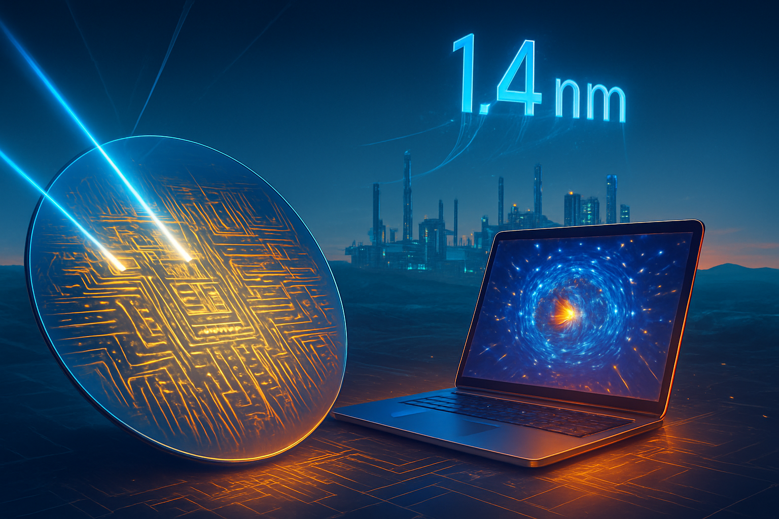
  • Intel Launches Panther Lake: The 18A ‘AI PC’ Era Officially Arrives at CES 2026

    Intel Launches Panther Lake: The 18A ‘AI PC’ Era Officially Arrives at CES 2026

    At the 2026 Consumer Electronics Show (CES) in Las Vegas, Intel CEO Lip-Bu Tan stood before a packed audience to unveil "Panther Lake," the company's most ambitious processor launch in a decade. Marketed as the Core Ultra Series 3, these chips represent more than just a seasonal refresh; they are the first high-volume consumer products built on the Intel 18A manufacturing process. This milestone signals the official arrival of the 18A era, a technological frontier Intel (NASDAQ: INTC) believes will reclaim its crown as the world’s leading semiconductor manufacturer.

    The significance of Panther Lake extends far beyond raw speed. By achieving a 60% performance-per-watt improvement over its predecessors, Intel is addressing the two biggest hurdles of the modern mobile era: battery life and heat. With major partners like Dell (NYSE: DELL) announcing that Panther Lake-powered hardware will begin shipping by late January 2026, the industry is witnessing a rapid shift toward "Local AI" devices that promise to handle complex workloads entirely on-device, fundamentally changing how consumers interact with their PCs.

    The Silicon Revolution: RibbonFET and PowerVia Meet 18A

    The technical foundation of Panther Lake is the Intel 18A node, which introduces two revolutionary structural changes to semiconductor design: RibbonFET and PowerVia. RibbonFET is Intel’s implementation of Gate-All-Around (GAA) transistors, replacing the FinFET architecture that has dominated the industry for over a decade. By wrapping the gate around all four sides of the channel, RibbonFET allows for precise control of the electrical current, significantly reducing leakage and enabling the transistors to operate at higher speeds while consuming less power.

    Complementing RibbonFET is PowerVia, the industry's first implementation of backside power delivery in consumer hardware. Traditionally, power and signal lines are bundled together above the transistor layer, creating electrical "noise" and congestion. PowerVia moves the power delivery to the underside of the silicon wafer, decoupling it from the data signals. This innovation reduces "voltage droop" and allows for a 10% increase in cell utilization, which directly translates to the massive efficiency gains Intel reported at the keynote.

    Under the hood, the flagship Panther Lake mobile processors feature a sophisticated 16-core hybrid architecture, combining "Cougar Cove" Performance-cores (P-cores) with "Darkmont" Efficiency-cores (E-cores). To meet the growing demands of generative AI, Intel has integrated its fifth-generation Neural Processing Unit (NPU 5), capable of delivering 50 TOPS (Trillions of Operations Per Second). Initial reactions from the research community have been overwhelmingly positive, with analysts noting that Intel has finally closed the "efficiency gap" that previously gave ARM-based competitors a perceived advantage in the thin-and-light laptop market.

    A High-Stakes Battle for the AI PC Market

    The launch of Panther Lake places immediate pressure on Intel’s chief rivals, AMD (NASDAQ: AMD) and Qualcomm (NASDAQ: QCOM). While AMD’s Ryzen AI 400 series currently offers competitive NPU performance, Intel’s move to the 18A node provides a manufacturing advantage that could lead to better margins and more consistent supply. Qualcomm, which saw significant gains in 2024 and 2025 with its Snapdragon X series, now faces an Intel that has successfully matched the power-sipping characteristics of ARM architecture with the broad software compatibility of x86.

    For tech giants like Microsoft (NASDAQ: MSFT), Panther Lake serves as the ideal vehicle for the next generation of Windows AI features. The 50 TOPS NPU meets the new, more stringent "Copilot+" requirements for 2026, enabling real-time video translation, advanced local coding assistants, and generative image editing without the latency or privacy concerns of the cloud. This shift is likely to disrupt existing SaaS models that rely on cloud-based AI, as more computing power moves to the "edge"—directly into the hands of the user.

    Furthermore, the success of the 18A process is a massive win for Intel Foundry. By proving that 18A can handle high-volume consumer silicon, Intel is sending a strong signal to potential customers like NVIDIA (NASDAQ: NVDA) and Apple (NASDAQ: AAPL). If Intel can maintain this lead, it may begin to siphon off high-end business from TSMC (NYSE: TSM), potentially altering the geopolitical and economic landscape of global chip production.

    Redefining the Broader AI Landscape

    The arrival of Panther Lake marks a pivotal moment in the transition from "AI as a service" to "AI as an interface." In the broader landscape, this development validates the industry's trend toward Small Language Models (SLMs) and on-device processing. As these processors become ubiquitous, the reliance on massive, energy-hungry data centers for basic AI tasks will diminish, potentially easing the strain on global energy grids and reducing the carbon footprint of the AI revolution.

    However, the rapid advancement of on-device AI also raises significant concerns regarding security and digital literacy. With Panther Lake making it easier than ever to run sophisticated deepfake and generative tools locally, the potential for misinformation grows. Experts have noted that while the hardware is ready, the legal and ethical frameworks for local AI are still in their infancy. This milestone mirrors previous breakthroughs like the transition to multi-core processing or the mobile internet revolution, where the technology arrived well before society fully understood its long-term implications.

    Compared to previous milestones, Panther Lake is being viewed as Intel’s "Ryzen moment"—a necessary and successful pivot that saves the company from irrelevance. By integrating RibbonFET and PowerVia simultaneously, Intel has leaped over several incremental steps that its competitors are still navigating. This technical "leapfrogging" is rare in the semiconductor world and suggests that the 18A node will be the benchmark against which all 2026 and 2027 hardware is measured.

    The Road Ahead: 14A and the Future of Computing

    Looking toward the future, Intel is already teasing the next step in its roadmap: the 14A node. While Panther Lake is the star of 2026, the company expects to begin initial "Clearwater Forest" production for data centers later this year, using an even more refined version of the 18A process. The ultimate goal is to achieve "system-on-wafer" designs where multiple chips are stacked and interconnected in ways that current manufacturing methods cannot support.

    Near-term developments will likely focus on software optimization. Now that the hardware can support 50+ TOPS, the challenge shifts to developers to create applications that justify that power. We expect to see a surge in specialized AI agents for creative professionals, researchers, and developers that can operate entirely offline. Experts predict that by 2027, the concept of a "Non-AI PC" will be as obsolete as a PC without an internet connection is today.

    Challenges remain, particularly regarding the global supply chain and the rising cost of advanced memory modules required to feed these high-speed processors. Intel will need to ensure that its foundry yields remain high to keep costs down for partners like Dell and HP. If they succeed, the 18A process will not just be a win for Intel, but a foundational technology for the next decade of personal computing.

    Conclusion: A New Chapter in Silicon History

    The launch of Panther Lake at CES 2026 is a definitive statement that Intel has returned to the forefront of semiconductor innovation. By successfully deploying 18A, RibbonFET, and PowerVia in a high-volume consumer product, Intel has silenced critics who doubted its "5 nodes in 4 years" strategy. The Core Ultra Series 3 is more than a processor; it is the cornerstone of a new era where AI is not an optional feature, but a fundamental component of the silicon itself.

    As we move into the first quarter of 2026, the industry will be watching the retail launch of Panther Lake laptops closely. The success of these devices will determine whether Intel can regain its dominant market share or if the competition from ARM and AMD has created a permanently fragmented PC market. Regardless of the outcome, the technological breakthroughs introduced today have set a new high-water mark for what is possible in mobile computing.

    For consumers and enterprises alike, the message is clear: the AI PC has evolved from a marketing buzzword into a powerful, efficient reality. With hardware shipping in just weeks, the 18A era has officially begun, and the world of computing will never be the same.


    This content is intended for informational purposes only and represents analysis of current AI developments.

    TokenRing AI delivers enterprise-grade solutions for multi-agent AI workflow orchestration, AI-powered development tools, and seamless remote collaboration platforms.
    For more information, visit https://www.tokenring.ai/.

  • Silicon Sovereignty: Intel Launches Panther Lake as the First US-Made 18A AI PC Powerhouse

    Silicon Sovereignty: Intel Launches Panther Lake as the First US-Made 18A AI PC Powerhouse

    In a landmark move for the American semiconductor industry, Intel Corporation (NASDAQ: INTC) has officially launched its "Panther Lake" processors at CES 2026, marking the first time a high-volume consumer AI PC platform has been manufactured using the cutting-edge Intel 18A process on U.S. soil. Branded as the Intel Core Ultra Series 3, these chips represent the completion of CEO Pat Gelsinger’s ambitious "five nodes in four years" strategy. The announcement signals a pivotal shift in the hardware race, as Intel seeks to reclaim its crown from global competitors by combining domestic manufacturing prowess with a massive leap in on-device artificial intelligence performance.

    The release of Panther Lake is more than just a seasonal hardware refresh; it is a declaration of silicon sovereignty. By moving the production of its flagship consumer silicon to Fab 52 in Chandler, Arizona, Intel is drastically reducing its reliance on overseas foundries. For the technology industry, the arrival of Panther Lake provides the primary hardware engine for the next generation of "Agentic AI"—software capable of performing complex, multi-step tasks autonomously on a user's laptop without needing to send sensitive data to the cloud.

    Engineering the 18A Breakthrough

    At the heart of Panther Lake lies the Intel 18A manufacturing process, a 1.8nm-class node that introduces two foundational innovations: RibbonFET and PowerVia. RibbonFET is Intel’s implementation of Gate-All-Around (GAA) transistor architecture, which replaces the long-standing FinFET design to provide superior control over electrical current, resulting in higher performance and lower power leakage. Complementing this is PowerVia, an industry-first backside power delivery system that moves power routing to the bottom of the silicon wafer. This decoupling of power and signal lines allows for significantly higher transistor density and up to a 30% reduction in multi-threaded power consumption compared to the previous generation.

    Technically, Panther Lake is a powerhouse of heterogeneous computing. The platform features the new "Cougar Cove" performance cores (P-cores) and "Darkmont" efficiency cores (E-cores), which together deliver a 50% boost in multi-threaded performance over the ultra-efficient Lunar Lake series. For AI workloads, the chips debut the NPU 5, a dedicated Neural Processing Unit capable of 50 Trillions of Operations Per Second (TOPS). When combined with the integrated Xe3 "Celestial" graphics engine—which contributes another 120 TOPS—the total platform AI throughput reaches a staggering 180 TOPS. This puts Panther Lake at the forefront of the industry, specifically optimized for running large language models (LLMs) and generative AI tools locally.

    Initial reactions from the hardware research community have been overwhelmingly positive, with analysts noting that Intel has finally closed the "efficiency gap" that had previously given an edge to ARM-based competitors. By achieving 27-hour battery life in reference designs while maintaining x86 compatibility, Intel has addressed the primary criticism of its mobile platforms. Industry experts highlight that the Xe3 GPU architecture is a particular standout, offering nearly double the gaming and creative performance of the previous Arc integrated graphics, effectively making discrete GPUs unnecessary for most mainstream professional users.

    Reshaping the Competitive Landscape

    The launch of Panther Lake creates immediate ripples across the tech sector, specifically challenging the recent incursions into the PC market by Qualcomm (NASDAQ: QCOM) and Apple (NASDAQ: AAPL). While Qualcomm’s Snapdragon X Elite series initially led the "Copilot+" PC wave in 2024 and 2025, Intel’s move to the 18A node brings x86 systems back to parity in power efficiency while maintaining a vast lead in software compatibility. This development is a boon for PC manufacturing giants like Dell Technologies (NYSE: DELL), HP Inc. (NYSE: HPQ), and Lenovo, who are now launching flagship products—such as the XPS 16 and ThinkPad X1 Carbon Gen 13—built specifically to leverage the Panther Lake architecture.

    Strategically, the success of 18A is a massive win for Intel’s fledgling foundry business. By proving that it can manufacture its own highest-end chips on 18A, Intel is sending a powerful signal to potential external customers like NVIDIA (NASDAQ: NVDA) and Microsoft (NASDAQ: MSFT). Microsoft, in particular, has already committed to using Intel’s 18A process for its own custom-designed silicon, and the stable rollout of Panther Lake validates that partnership. Intel is no longer just a chip designer; it is re-emerging as a world-class manufacturer that can compete head-to-head with TSMC (NYSE: TSM) for the world’s most advanced AI hardware.

    The competitive pressure is now shifting back to Advanced Micro Devices (NASDAQ: AMD), whose upcoming Ryzen AI "Gorgon Point" chips will need to match Intel’s 18A density and the 50 TOPS NPU baseline. While AMD currently holds a slight lead in raw multi-core efficiency in some segments, Intel’s "Foundry First" approach gives it more control over its supply chain and margins. For startups and software developers in the AI space, the ubiquity of 180-TOPS "Panther Lake" laptops means that the addressable market for sophisticated, local AI applications is set to explode in 2026.

    Geopolitics and the New AI Standard

    The wider significance of Panther Lake extends into the realm of global economics and national security. As the first leading-edge AI chip manufactured at scale in the United States, Panther Lake is the "poster child" for the CHIPS and Science Act. It represents a reversal of decades of semiconductor manufacturing moving to East Asia. For government and enterprise customers, the "Made in USA" aspect of the 18A process offers a level of supply chain transparency and security that is increasingly critical in an era of heightened geopolitical tension.

    Furthermore, Panther Lake sets a new standard for what constitutes an "AI PC." We are moving beyond simple background blur in video calls and toward "Agentic AI," where the computer acts as a proactive assistant. With 50 TOPS available on the NPU alone, Panther Lake can run highly quantized versions of Llama 3 or Mistral models locally, ensuring that user data never leaves the device. This local-first approach to AI addresses growing privacy concerns and the massive energy costs associated with cloud-based AI processing.

    Comparing this to previous milestones, Panther Lake is being viewed as Intel’s "Centrino moment" for the AI era. Just as Centrino integrated Wi-Fi and defined the modern mobile laptop in 2003, Panther Lake integrates high-performance AI acceleration as a default, non-negotiable feature of the modern PC. It marks the transition from AI as an experimental add-on to AI as a fundamental layer of the operating system and user experience.

    The Horizon: Beyond 18A

    Looking ahead, the roadmap following Panther Lake is already coming into focus. Intel has already begun early work on "Nova Lake," expected in late 2026 or early 2027, which will likely utilize the even more advanced Intel 14A process. The near-term challenge for Intel will be the rapid ramp-up of production at its Arizona and Ohio facilities to meet the expected demand for the Core Ultra Series 3. Experts predict that as software developers begin to target the 50 TOPS NPU floor, we will see a new category of "AI-native" applications that were previously impossible on mobile hardware.

    Potential applications on the horizon include real-time, zero-latency language translation during live meetings, automated local coding assistants that understand an entire local codebase, and generative video editing tools that run entirely on the laptop's battery. However, the industry must still address the challenge of "AI fragmentation"—ensuring that developers can easily write code that runs across Intel, AMD, and Qualcomm NPUs. Intel’s OpenVINO toolkit is expected to play a crucial role in standardizing this experience.

    A New Era for Intel and the AI PC

    In summary, the launch of Panther Lake is a defining moment for Intel and the broader technology landscape. It marks the successful execution of a high-stakes manufacturing gamble and restores Intel’s position as a leader in semiconductor innovation. By delivering 50 NPU TOPS and a massive leap in graphics and efficiency through the 18A process, Intel has effectively raised the bar for what consumers and enterprises should expect from their hardware.

    The historical significance of this development cannot be overstated; it is the first time in over a decade that Intel has held a clear lead in transistor technology while simultaneously localized production in the United States. As laptops powered by Panther Lake begin shipping to consumers on January 27, 2026, the industry will be watching closely to see how the software ecosystem responds. For now, the "AI PC" has moved from a marketing buzzword to a high-performance reality, and the race for silicon supremacy has entered its most intense chapter yet.


    This content is intended for informational purposes only and represents analysis of current AI developments.

    TokenRing AI delivers enterprise-grade solutions for multi-agent AI workflow orchestration, AI-powered development tools, and seamless remote collaboration platforms.
    For more information, visit https://www.tokenring.ai/.