Tag: Power Chips

  • GlobalFoundries and TSMC Forge Landmark GaN Alliance, Reshaping US Power Chip Manufacturing

    GlobalFoundries and TSMC Forge Landmark GaN Alliance, Reshaping US Power Chip Manufacturing

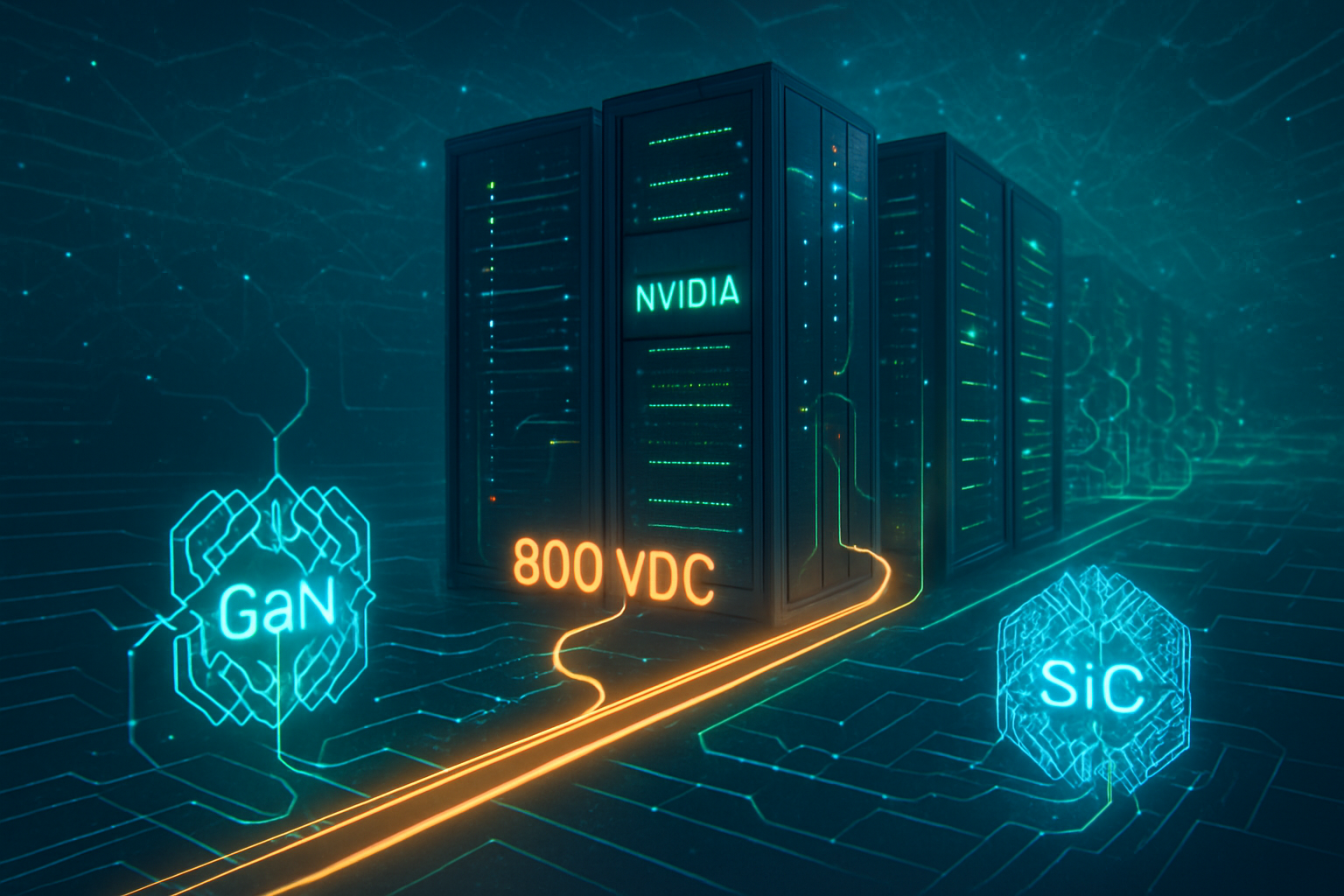
    In a pivotal development set to redefine the landscape of power semiconductor manufacturing, GlobalFoundries (NASDAQ: GFS) announced on November 10, 2025, a significant technology licensing agreement with Taiwan Semiconductor Manufacturing Company (NYSE: TSM). This strategic partnership focuses on advanced Gallium Nitride (GaN) technology, specifically 650V and 80V platforms, and is poised to dramatically accelerate GlobalFoundries' development and U.S.-based production of next-generation GaN power chips. The immediate significance lies in fortifying the domestic supply chain for critical power components, addressing burgeoning demand across high-growth sectors.

    This collaboration emerges at a crucial juncture, as TSMC, a global foundry leader, prepares to strategically exit its broader GaN foundry services by July 2027 to intensify its focus on advanced-node silicon for AI applications and advanced packaging. GlobalFoundries' acquisition of this proven GaN expertise not only ensures the continued availability and advancement of the technology but also strategically positions its Burlington, Vermont, facility as a vital hub for U.S.-manufactured GaN semiconductors, bolstering national efforts towards semiconductor independence and resilience.

    Technical Prowess: Unpacking the Advanced GaN Technology

    The licensed technology from TSMC encompasses both 650V and 80V GaN-on-Silicon (GaN-on-Si) capabilities. GlobalFoundries will leverage its existing high-voltage GaN-on-Silicon expertise at its Burlington facility to integrate and scale this technology, with a strong focus on 200mm (8-inch) wafer manufacturing for high-volume production. This move is particularly impactful as TSMC had previously developed robust second-generation GaN-on-Si processes, and GlobalFoundries is now gaining access to this established and validated technology.

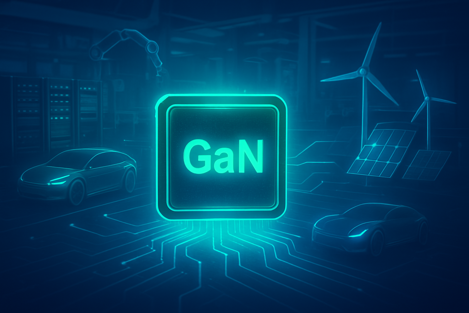
    GaN technology offers substantial performance advantages over traditional silicon-based semiconductors in power applications due to its wider bandgap. Key differentiators include significantly higher energy efficiency and power density, enabling smaller, more compact designs. GaN devices boast faster switching speeds—up to 10 times faster than silicon MOSFETs and 100 times faster than IGBTs—which allows for higher operating frequencies and smaller passive components. Furthermore, GaN exhibits superior thermal performance, efficiently dissipating heat and reducing the need for complex cooling systems.

    Unlike previous approaches that relied heavily on silicon, which is reaching its performance limits in terms of efficiency and power density, GaN provides a critical leap forward. While Silicon Carbide (SiC) is another wide bandgap material, GaN-on-Silicon offers a cost-effective solution for operating voltages below 1000V by utilizing existing silicon manufacturing infrastructure. Initial reactions from the semiconductor research community and industry experts have been largely positive, viewing this as a strategic win for GlobalFoundries and a significant step towards strengthening the U.S. domestic semiconductor ecosystem, especially given TSMC's strategic pivot.

    The technology is targeted for high-performance, energy-efficient applications across various sectors, including power management solutions for data centers, industrial power applications, and critical components for electric vehicles (EVs) such as onboard chargers and DC-DC converters. It also holds promise for renewable energy systems, fast-charging electronics, IoT devices, and even aerospace and defense applications requiring robust RF and high-power control. GlobalFoundries emphasizes a holistic approach to GaN reliability, designing for harsh environments to ensure robustness and longevity.

    Market Ripple Effects: Impact on the Semiconductor Industry

    This strategic partnership carries profound implications for semiconductor companies, tech giants, and startups alike. GlobalFoundries (NASDAQ: GFS) stands as the primary beneficiary, gaining rapid access to proven GaN technology that will significantly accelerate its GaN roadmap and bolster its position as a leading contract manufacturer. This move allows GF to address the growing demand for higher efficiency and power density in power systems, offering a crucial U.S.-based manufacturing option for GaN-on-silicon semiconductors.

    For other semiconductor companies, the landscape is shifting. Companies that previously relied on TSMC (NYSE: TSM) for GaN foundry services, such as Navitas Semiconductor (NASDAQ: NVTS) and ROHM (TSE: 6963), have already begun seeking alternative manufacturing partners due to TSMC's impending exit. GlobalFoundries, with its newly acquired technology and planned U.S. production, is now poised to become a key alternative foundry, potentially capturing a significant portion of this reallocated business. This intensifies competition for established players like Infineon Technologies (OTC: IFNNY) and Innoscience, which are also major forces in the power semiconductor and GaN markets.

    Tech giants involved in cloud computing, electric vehicles, and advanced industrial equipment stand to benefit from a more diversified and robust GaN supply chain. The increased manufacturing capacity and technological expertise at GlobalFoundries will lead to a wider availability of GaN power devices, enabling these companies to integrate more energy-efficient and compact designs into their products. For startups focused on innovative GaN-based power management solutions, GlobalFoundries' entry provides a reliable manufacturing partner, potentially lowering barriers to entry and accelerating time-to-market.

    The primary disruption stems from TSMC's withdrawal from GaN foundry services, which necessitates a transition for its current GaN customers. However, GlobalFoundries' timely entry with licensed TSMC technology can mitigate some of this disruption by offering a familiar and proven process. This development significantly bolsters U.S.-based manufacturing capabilities for advanced semiconductors, enhancing market positioning and strategic advantages for GlobalFoundries by offering U.S.-based GaN capacity to a global customer base, aligning with national initiatives to strengthen domestic chip production.

    Broader Significance: A New Era for Power Electronics

    The GlobalFoundries and TSMC GaN technology licensing agreement signifies a critical juncture in the broader semiconductor manufacturing landscape, underscoring a decisive shift towards advanced materials and enhanced supply chain resilience. This partnership accelerates the adoption of GaN, a "third-generation" semiconductor material, which offers superior performance characteristics over traditional silicon, particularly in high-power and high-frequency applications. Its ability to deliver higher efficiency, faster switching speeds, and better thermal management is crucial as silicon-based CMOS technologies approach their fundamental limits.

    This move fits perfectly into current trends driven by the surging demand from next-generation technologies such as 5G telecommunications, electric vehicles, data centers, and renewable energy systems. The market for GaN semiconductor devices is projected for substantial growth, with some estimates predicting the power GaN market to reach approximately $3 billion by 2030. The agreement's emphasis on establishing U.S.-based GaN capacity directly addresses pressing concerns about supply chain resilience, especially given the geopolitical sensitivity surrounding raw materials like gallium. Diversifying manufacturing locations for critical components is a top priority for national security and economic stability.

    The impacts on global chip production are multifaceted. It promises increased availability and competition in the GaN market, offering customers an additional U.S.-based manufacturing option that could reduce lead times and geopolitical risks. This expanded capacity will enable more widespread integration of GaN into new product designs across various industries, leading to more efficient and compact electronic systems. While intellectual property (IP) is always a concern in such agreements, the history of cross-licensing and cooperation between TSMC and GlobalFoundries suggests a framework for managing such issues, allowing both companies freedom to operate and innovate.

    Comparisons to previous semiconductor industry milestones are apt. This shift from silicon to GaN for specific applications mirrors the earlier transition from germanium to silicon in the early days of transistors, driven by superior material properties. It represents a "vertical" advancement in material capability, distinct from the "horizontal" scaling achieved through lithography advancements, promising to enable new generations of power-efficient devices. This strategic collaboration also highlights the industry's evolving approach to IP, where licensing agreements facilitate technological progress rather than being bogged down by disputes.

    The Road Ahead: Future Developments and Challenges

    The GlobalFoundries and TSMC GaN partnership heralds significant near-term and long-term developments for advanced GaN power chips. In the near term, development of the licensed technology is slated to commence in early 2026 at GlobalFoundries' Burlington, Vermont facility, with initial production expected to ramp up later that year. This rapid integration aims to quickly bring high-performance GaN solutions to market, leveraging GlobalFoundries' existing expertise and significant federal funding (over $80 million since 2020) dedicated to advancing GaN-on-silicon manufacturing in the U.S.

    Long-term, the partnership is set to deliver GaN chips that will address critical power gaps across mission-critical applications in data centers, automotive, and industrial sectors. The comprehensive GaN portfolio GlobalFoundries is developing, designed for harsh environments and emphasizing reliability, will solidify GaN's role as a next-generation solution for achieving higher efficiency, power density, and compactness where traditional silicon CMOS technologies approach their limits.

    Potential applications and use cases for these advanced GaN power chips are vast and transformative. In Artificial Intelligence (AI), GaN is crucial for meeting the exponential energy demands of AI data centers, enabling power supplies to evolve for higher computational power within reduced footprints. For Electric Vehicles (EVs), GaN promises extended range and faster charging capabilities through smaller, lighter, and more efficient power conversion systems in onboard chargers and DC-DC converters, with future potential in traction inverters. In Renewable Energy, GaN will enhance energy conversion efficiency in solar inverters, wind turbine systems, and overall grid infrastructure, contributing to grid stability and decarbonization efforts.

    Despite its promising future, GaN technology faces challenges, particularly concerning U.S.-based manufacturing capabilities. These include the higher initial cost of GaN components, the complexities of manufacturing scalability and yield (such as lattice mismatch defects when growing GaN on silicon), and ensuring long-term reliability in harsh operating environments. A critical challenge for the U.S. is the current lack of sufficient domestic epitaxy capacity, a crucial step in GaN production, necessitating increased investment to secure the supply chain.

    Experts predict a rapid expansion of the GaN market, with significant growth projected through 2030 and beyond, driven by AI and electrification. GaN is expected to displace legacy silicon in many high-power applications, becoming ubiquitous in power conversion stages from consumer devices to grid-scale energy storage. Future innovations will focus on increased integration, with GaN power FETs combined with control, drive, sensing, and protection circuitry into single, high-performance GaN ICs. The transition to larger wafer sizes (300mm) and advancements in vertical GaN technology are also anticipated to further enhance efficiency and cost-effectiveness.

    A New Chapter in US Chip Independence

    The GlobalFoundries and TSMC GaN technology licensing agreement marks a monumental step, not just for the companies involved, but for the entire semiconductor industry and the broader global economy. The key takeaway is the strategic acceleration of U.S.-based GaN manufacturing, driven by a world-class technology transfer. This development is profoundly significant in the context of semiconductor manufacturing history, representing a critical shift towards advanced materials and a proactive approach to supply chain resilience.

    Its long-term impact on U.S. chip independence and technological advancement is substantial. By establishing a robust domestic hub for advanced GaN production at GlobalFoundries' Vermont facility, the U.S. gains greater control over the manufacturing of essential components for strategic sectors like defense, electric vehicles, and renewable energy. This not only enhances national security but also fosters innovation within the U.S. semiconductor ecosystem, driving economic growth and creating high-tech jobs.

    In the coming weeks and months, industry observers and consumers should closely watch for GlobalFoundries' qualification and production milestones at its Vermont facility in early 2026, followed by the availability of initial products later that year. Monitor customer adoption and design wins, particularly in the data center, industrial, and automotive sectors, as these will be crucial indicators of market acceptance. Keep an eye on the evolving GaN market pricing and competition, especially with TSMC's exit and the continued pressure from other global players. Finally, continued U.S. government support and broader technological advancements in GaN, such as larger wafer sizes and new integration techniques, will be vital to watch for as this partnership unfolds and shapes the future of power electronics.


    This content is intended for informational purposes only and represents analysis of current AI developments.

    TokenRing AI delivers enterprise-grade solutions for multi-agent AI workflow orchestration, AI-powered development tools, and seamless remote collaboration platforms.
    For more information, visit https://www.tokenring.ai/.

  • Navitas Semiconductor Unveils 800V Power Solutions, Propelling NVIDIA’s Next-Gen AI Data Centers

    Navitas Semiconductor Unveils 800V Power Solutions, Propelling NVIDIA’s Next-Gen AI Data Centers

    Navitas Semiconductor (NASDAQ: NVTS) today, October 13, 2025, announced a pivotal advancement in its power chip technology, unveiling new gallium nitride (GaN) and silicon carbide (SiC) devices specifically engineered to support NVIDIA's (NASDAQ: NVDA) groundbreaking 800 VDC power architecture. This development is critical for enabling the next generation of AI computing platforms and "AI factories," which face unprecedented power demands. The immediate significance lies in facilitating a fundamental architectural shift within data centers, moving away from traditional 54V systems to meet the multi-megawatt rack densities required by cutting-edge AI workloads, promising enhanced efficiency, scalability, and reduced infrastructure costs for the rapidly expanding AI sector.

    This strategic move by Navitas is set to redefine power delivery for high-performance AI, ensuring that the physical and economic constraints of powering increasingly powerful AI processors do not impede the industry's relentless pace of innovation. By addressing the core challenge of efficient energy distribution, Navitas's solutions are poised to unlock new levels of performance and sustainability for AI infrastructure globally.

    Technical Prowess: Powering the AI Revolution with GaN and SiC

    Navitas's latest portfolio introduces a suite of high-performance power devices tailored for NVIDIA's demanding AI infrastructure. Key among these are the new 100 V GaN FETs, meticulously optimized for the lower-voltage DC-DC stages found on GPU power boards. These GaN-on-Si field-effect transistors are fabricated using a 200 mm process through a strategic partnership with Power Chip, ensuring scalable, high-volume manufacturing. Designed with advanced dual-sided cooled packages, these FETs directly tackle the critical needs for ultra-high power density and superior thermal management in next-generation AI compute platforms, where individual AI chips can consume upwards of 1000W.

    Complementing the 100 V GaN FETs, Navitas has also enhanced its 650 V GaN portfolio with new high-power GaN FETs and advanced GaNSafe™ power ICs. The GaNSafe™ devices integrate crucial control, drive, sensing, and built-in protection features, offering enhanced robustness and reliability vital for demanding AI infrastructure. These components boast ultra-fast short-circuit protection with a 350 ns response time, 2 kV ESD protection, and programmable slew-rate control, ensuring stable and secure operation in high-stress environments. Furthermore, Navitas continues to leverage its High-Voltage GeneSiC™ SiC MOSFET lineup, providing silicon carbide MOSFETs ranging from 650 V to 6,500 V, which support various stages of power conversion across the broader data center infrastructure.

    This technological leap fundamentally differs from previous approaches by enabling NVIDIA's recently announced 800 VDC power architecture. Unlike traditional 54V in-rack power distribution systems, the 800 VDC architecture allows for direct conversion from 13.8 kVAC utility power to 800 VDC at the data center perimeter. This eliminates multiple conventional AC/DC and DC/DC conversion stages, drastically maximizing energy efficiency and reducing resistive losses. Navitas's solutions are capable of achieving PFC peak efficiencies of up to 99.3%, a significant improvement that directly translates to lower operational costs and a smaller carbon footprint. The shift also reduces copper wire thickness by up to 45% due to lower current, leading to material cost savings and reduced weight.

    Initial reactions from the AI research community and industry experts underscore the critical importance of these advancements. While specific, in-depth reactions to this very recent announcement are still emerging, the consensus emphasizes the pivotal role of wide-bandbandgap (WBG) semiconductors like GaN and SiC in addressing the escalating power and thermal challenges of AI data centers. Experts consistently highlight that power delivery has become a significant bottleneck for AI's growth, with AI workloads consuming substantially more power than traditional computing. The industry widely recognizes NVIDIA's strategic shift to 800 VDC as a necessary architectural evolution, with other partners like ABB (SWX: ABBN) and Infineon (FWB: IFX) also announcing support, reinforcing the widespread need for higher voltage systems to enhance efficiency, scalability, and reliability.

    Strategic Implications: Reshaping the AI Industry Landscape

    Navitas Semiconductor's integral role in powering NVIDIA's 800 VDC AI platforms is set to profoundly impact various players across the AI industry. Hyperscale cloud providers and AI factory operators, including tech giants like Alphabet (NASDAQ: GOOGL), Amazon (NASDAQ: AMZN), Meta Platforms (NASDAQ: META), Microsoft (NASDAQ: MSFT), and Oracle Cloud Infrastructure (NYSE: ORCL), alongside specialized AI infrastructure providers such as CoreWeave, Lambda, Nebius, and Together AI, stand as primary beneficiaries. The enhanced power efficiency, increased power density, and improved thermal performance offered by Navitas's chips will lead to substantial reductions in operational costs—energy, cooling, and maintenance—for these companies. This translates directly to a lower total cost of ownership (TCO) for AI infrastructure, enabling them to scale their AI operations more economically and sustainably.

    AI model developers and researchers will benefit indirectly from the more robust and efficient infrastructure. The ability to deploy higher power density racks means more GPUs can be integrated into a smaller footprint, significantly accelerating training times and enabling the development of even larger and more capable AI models. This foundational improvement is crucial for fueling continued innovation in areas such as generative AI, large language models, and advanced scientific simulations, pushing the boundaries of what AI can achieve.

    For AI hardware manufacturers and data center infrastructure providers, such as HPE (NYSE: HPE), Vertiv (NYSE: VRT), and Foxconn (TPE: 2317), the shift to the 800 VDC architecture necessitates adaptation. Companies that swiftly integrate these new power management solutions, leveraging the superior characteristics of GaN and SiC, will gain a significant competitive advantage. Vertiv, for instance, has already unveiled its 800 VDC MGX reference architecture, demonstrating proactive engagement with this evolving standard. This transition also presents opportunities for startups specializing in cooling, power distribution, and modular data center solutions to innovate within the new architectural paradigm.

    Navitas Semiconductor's collaboration with NVIDIA significantly bolsters its market positioning. As a pure-play wide-bandgap power semiconductor company, Navitas has validated its technology for high-performance, high-growth markets like AI data centers, strategically expanding beyond its traditional strength in consumer fast chargers. This partnership positions Navitas as a critical enabler of this architectural shift, particularly with its specialized 100V GaN FET portfolio and high-voltage SiC MOSFETs. While the power semiconductor market remains highly competitive, with major players like Infineon, STMicroelectronics (NYSE: STM), Texas Instruments (NASDAQ: TXN), and OnSemi (NASDAQ: ON) also developing GaN and SiC solutions, Navitas's specific focus and early engagement with NVIDIA provide a strong foothold. The overall wide-bandgap semiconductor market is projected for substantial growth, ensuring intense competition and continuous innovation.

    Wider Significance: A Foundational Shift for Sustainable AI

    This development by Navitas Semiconductor, enabling NVIDIA's 800 VDC AI platforms, represents more than just a component upgrade; it signifies a fundamental architectural transformation within the broader AI landscape. It directly addresses the most pressing challenge facing the exponential growth of AI: scalable and efficient power delivery. As AI workloads continue to surge, demanding multi-megawatt rack densities that traditional 54V systems cannot accommodate, the 800 VDC architecture becomes an indispensable enabler for the "AI factories" of the future. This move aligns perfectly with the industry trend towards higher power density, greater energy efficiency, and simplified power distribution to support the insatiable demands of AI processors that can exceed 1,000W per chip.

    The impacts on the industry are profound, leading to a complete overhaul of data center design. This shift will result in significant reductions in operational costs for AI infrastructure providers due to improved energy efficiency (up to 5% end-to-end) and reduced cooling requirements. It is also crucial for enabling the next generation of AI hardware, such as NVIDIA's Rubin Ultra platform, by ensuring that these powerful accelerators receive the necessary, reliable power. On a societal level, this advancement contributes significantly to addressing the escalating energy consumption and environmental concerns associated with AI. By making AI infrastructure more sustainable, it helps mitigate the carbon footprint of AI, which is projected to consume a substantial portion of global electricity in the coming years.

    However, this transformative shift is not without its concerns. Implementing 800 VDC systems introduces new complexities related to electrical safety, insulation, and fault management within data centers. There's also the challenge of potential supply chain dependence on specialized GaN and SiC power semiconductors, though Navitas's partnership with Power Chip for 200mm GaN-on-Si production aims to mitigate this. Thermal management remains a critical issue despite improved electrical efficiency, necessitating advanced liquid cooling solutions for ultra-high power density racks. Furthermore, while efficiency gains are crucial, there is a risk of a "rebound effect" (Jevon's paradox), where increased efficiency might lead to even greater overall energy consumption due to expanded AI deployment and usage, placing unprecedented demands on energy grids.

    In terms of historical context, this development is comparable to the pivotal transition from CPUs to GPUs for AI, which provided orders of magnitude improvements in computational power. While not an algorithmic breakthrough itself, Navitas's power chips are a foundational infrastructure enabler, akin to the early shifts to higher voltage (e.g., 12V to 48V) in data centers, but on a far grander scale. It also echoes the continuous development of specialized AI accelerators and the increasing necessity of advanced cooling solutions. Essentially, this power management innovation is a critical prerequisite, allowing the AI industry to overcome physical limitations and continue its rapid advancement and societal impact.

    The Road Ahead: Future Developments in AI Power Management

    In the near term, the focus will be on the widespread adoption and refinement of the 800 VDC architecture, leveraging Navitas's advanced GaN and SiC power devices. Navitas is actively progressing its "AI Power Roadmap," which aims to rapidly increase server power platforms from 3kW to 12kW and beyond. The company has already demonstrated an 8.5kW AI data center PSU powered by GaN and SiC, achieving 98% efficiency and complying with Open Compute Project (OCP) and Open Rack v3 (ORv3) specifications. Expect continued innovation in integrated GaNSafe™ power ICs, offering further advancements in control, drive, sensing, and protection, crucial for the robustness of future AI factories.

    Looking further ahead, the potential applications and use cases for these high-efficiency power solutions extend beyond just hyperscale AI data centers. While "AI factories" remain the primary target, the underlying wide bandgap technologies are also highly relevant for industrial platforms, advanced energy storage systems, and grid-tied inverter projects, where efficiency and power density are paramount. The ability to deliver megawatt-scale power with significantly more compact and reliable solutions will facilitate the expansion of AI into new frontiers, including more powerful edge AI deployments where space and power constraints are even more critical.

    However, several challenges need continuous attention. The exponentially growing power demands of AI will remain the most significant hurdle; even with 800 VDC, the sheer scale of anticipated AI factories will place immense strain on energy grids. The "readiness gap" in existing data center ecosystems, many of which cannot yet support the power demands of the latest NVIDIA GPUs, requires substantial investment and upgrades. Furthermore, ensuring robust and efficient thermal management for increasingly dense AI racks will necessitate ongoing innovation in liquid cooling technologies, such as direct-to-chip and immersion cooling, which can reduce cooling energy requirements by up to 95%.

    Experts predict a dramatic surge in data center power consumption, with Goldman Sachs Research forecasting a 50% increase by 2027 and up to 165% by the end of the decade compared to 2023. This necessitates a "power-first" approach to data center site selection, prioritizing access to substantial power capacity. The integration of renewable energy sources, on-site generation, and advanced battery storage will become increasingly critical to meet these demands sustainably. The evolution of data center design will continue towards higher power densities, with racks reaching up to 30 kW by 2027 and even 120 kW for specific AI training models, fundamentally reshaping the physical and operational landscape of AI infrastructure.

    A New Era for AI Power: Concluding Thoughts

    Navitas Semiconductor's announcement on October 13, 2025, regarding its new GaN and SiC power chips for NVIDIA's 800 VDC AI platforms marks a monumental leap forward in addressing the insatiable power demands of artificial intelligence. The key takeaway is the enablement of a fundamental architectural shift in data center power delivery, moving from the limitations of 54V systems to a more efficient, scalable, and reliable 800 VDC infrastructure. This transition, powered by Navitas's advanced wide bandgap semiconductors, promises up to 5% end-to-end efficiency improvements, significant reductions in copper usage, and simplified power trains, directly supporting NVIDIA's vision of multi-megawatt "AI factories."

    This development's significance in AI history cannot be overstated. While not an AI algorithmic breakthrough, it is a critical foundational enabler that allows the continuous scaling of AI computational power. Without such innovations in power management, the physical and economic limits of data center construction would severely impede the advancement of AI. It represents a necessary evolution, akin to past shifts in computing architecture, but driven by the unprecedented energy requirements of modern AI. This move is crucial for the sustained growth of AI, from large language models to complex scientific simulations, and for realizing the full potential of AI's societal impact.

    The long-term impact will be profound, shaping the future of AI infrastructure to be more efficient, sustainable, and scalable. It will reduce operational costs for AI operators, contribute to environmental responsibility by lowering AI's carbon footprint, and spur further innovation in power electronics across various industries. The shift to 800 VDC is not merely an upgrade; it's a paradigm shift that redefines how AI is powered, deployed, and scaled globally.

    In the coming weeks and months, the industry should closely watch for the implementation of this 800 VDC architecture in new AI factories and data centers, with particular attention to initial performance benchmarks and efficiency gains. Further announcements from Navitas regarding product expansions and collaborations within the rapidly growing 800 VDC ecosystem will be critical. The broader adoption of new industry standards for high-voltage DC power delivery, championed by organizations like the Open Compute Project, will also be a key indicator of this architectural shift's momentum. The evolution of AI hinges on these foundational power innovations, making Navitas's role in this transformation one to watch closely.


    This content is intended for informational purposes only and represents analysis of current AI developments.

    TokenRing AI delivers enterprise-grade solutions for multi-agent AI workflow orchestration, AI-powered development tools, and seamless remote collaboration platforms.
    For more information, visit https://www.tokenring.ai/.