Tag: Power Semiconductors

  • The 1,000,000-Watt Rack: Mitsubishi Electric Breakthrough in Trench SiC MOSFETs Solves AI’s Power Paradox

    The 1,000,000-Watt Rack: Mitsubishi Electric Breakthrough in Trench SiC MOSFETs Solves AI’s Power Paradox

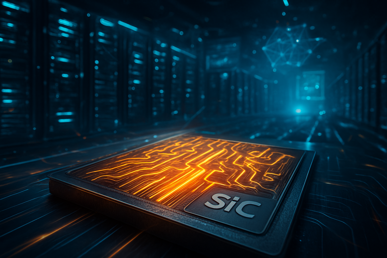
    In a move that signals a paradigm shift for high-density computing and sustainable transport, Mitsubishi Electric Corp (TYO: 6503) has announced a major breakthrough in Wide-Bandgap (WBG) power semiconductors. On January 14, 2026, the company revealed it would begin sample shipments of its next-generation trench Silicon Carbide (SiC) MOSFET bare dies on January 21. These chips, which utilize a revolutionary "trench" architecture, represent a 50% reduction in power loss compared to traditional planar SiC devices, effectively removing one of the primary thermal bottlenecks currently capping the growth of artificial intelligence and electric vehicle performance.

    The announcement comes at a critical juncture as the technology industry grapples with the energy-hungry nature of generative AI. With the latest AI-accelerated server racks now demanding up to 1 megawatt (1MW) of power, traditional silicon-based power conversion has hit a physical "efficiency wall." Mitsubishi Electric's new trench SiC technology is designed to operate in these extreme high-density environments, offering superior heat resistance and efficiency that allows power modules to shrink in size while handling significantly higher voltages. This development is expected to accelerate the deployment of next-generation data centers and extend the range of electric vehicles (EVs) by as much as 7% through more efficient traction inverters.

    Technical Superiority: The Trench Architecture Revolution

    At the heart of Mitsubishi Electric’s breakthrough is the transition from a "planar" gate structure to a "trench" design. In a traditional planar MOSFET, electricity flows horizontally across the surface of the chip before moving vertically, a path that inherently creates higher resistance and limits chip density. Mitsubishi’s new trench SiC-MOSFETs utilize a proprietary "oblique ion implantation" method. By implanting nitrogen in a specific diagonal orientation, the company has created a high-concentration layer that allows electricity to flow more easily through vertical channels. This innovation has resulted in a world-leading specific ON-resistance of approximately 1.84 mΩ·cm², a metric that translates directly into lower heat generation and higher efficiency.

    Technical specifications for the initial four models (WF0020P-0750AA through WF0080P-0750AA) indicate a rated voltage of 750V with ON-resistance ranging from 20 mΩ to 80 mΩ. Beyond mere efficiency, Mitsubishi has solved the "reliability gap" that has long plagued trench SiC devices. Trench structures are notorious for concentrated electric fields at the bottom of the "V" or "U" shape, which can degrade the gate-insulating film over time. To counter this, Mitsubishi engineers developed a unique electric-field-limiting structure by vertically implanting aluminum at the bottom of the trench. This protective layer reduces field stress to levels comparable to older planar devices, ensuring a stable lifecycle even under the high-speed switching demands of AI power supply units (PSUs).

    The industry reaction has been overwhelmingly positive, with power electronics researchers noting that Mitsubishi's focus on bare dies is a strategic masterstroke. By providing the raw chips rather than finished modules, Mitsubishi is allowing companies like NVIDIA Corp (NASDAQ: NVDA) and high-end EV manufacturers to integrate these power-dense components directly into custom liquid-cooled power shelves. Experts suggest that the 50% reduction in switching losses will be the deciding factor for engineers designing the 12kW+ power supplies required for the latest "Rubin" class GPUs, where every milliwatt saved reduces the massive cooling overhead of 1MW data center racks.

    Market Warfare: The Race for 200mm Dominance

    The release of these trench MOSFETs places Mitsubishi Electric in direct competition with a field of energized rivals. STMicroelectronics (NYSE: STM) currently holds the largest market share in the SiC space and is rapidly scaling its own 200mm (8-inch) wafer production in Italy and China. Similarly, Infineon Technologies AG (OTC: IFNNY) has recently brought its massive Kulim, Malaysia fab online, focusing on "CoolSiC" Gen2 trench devices. However, Mitsubishi’s proprietary gate oxide stability and its "bare die first" delivery strategy for early 2026 may give it a temporary edge in the high-performance "boutique" sector of the market, specifically for 800V EV architectures.

    The competitive landscape is also seeing a resurgence from Wolfspeed, Inc. (NYSE: WOLF), which recently emerged from a major restructuring to focus exclusively on its Mohawk Valley 8-inch fab. Meanwhile, ROHM Co., Ltd. (TYO: 6963) has been aggressive in the Japanese and Chinese markets with its 5th-generation trench designs. Mitsubishi’s entry into mass-production sample shipments marks a "normalization" of the 200mm SiC era, where increased yields are finally beginning to lower the "SiC tax"—the premium price that has historically kept Wide-Bandgap materials out of mid-range consumer electronics.

    Strategically, Mitsubishi is positioning itself as the go-to partner for the Open Compute Project (OCP) standards. As hyperscalers like Google and Meta move toward 1MW racks, they are shifting from 48V DC power distribution to high-voltage DC (HVDC) systems of 400V or 800V. Mitsubishi’s 750V-rated trench dies are perfectly positioned for the DC-to-DC conversion stages in these environments. By drastically reducing the footprint of the power infrastructure—sometimes by as much as 75% compared to silicon—Mitsubishi is enabling data center operators to pack more compute into the same physical square footage, a move that is essential for the survival of the current AI boom.

    Beyond the Chips: Solving the AI Sustainability Crisis

    The broader significance of this breakthrough cannot be overstated: it is a direct response to the "AI Power Crisis." The current generation of AI hardware, such as the Advanced Micro Devices, Inc. (NASDAQ: AMD) Instinct MI355X and NVIDIA’s Blackwell systems, has pushed the power density of data centers to a breaking point. A single AI rack in 2026 can consume as much electricity as a small town. Without the efficiency gains provided by Wide-Bandgap materials like SiC, the thermal load would require cooling systems so massive they would negate the economic benefits of the AI models themselves.

    This milestone is being compared to the transition from vacuum tubes to transistors in the mid-20th century. Just as the transistor allowed for the miniaturization of computers, SiC is allowing for the "miniaturization of power." By achieving 98% efficiency in power conversion, Mitsubishi's technology ensures that less energy is wasted as heat. This has profound implications for global sustainability goals; even a 1% increase in efficiency across the global data center fleet could save billions of kilowatt-hours annually.

    However, the rapid shift to SiC is not without concerns. The industry remains wary of supply chain bottlenecks, as the raw material—silicon carbide boules—is significantly harder to grow than standard silicon. Furthermore, the high-speed switching of SiC can create electromagnetic interference (EMI) issues in sensitive AI server environments. Mitsubishi’s unique gate oxide manufacturing process aims to address some of these reliability concerns, but the integration of these high-frequency components into existing legacy infrastructure remains a challenge for the broader engineering community.

    The Horizon: 2kV Chips and the End of Silicon

    Looking toward the late 2020s, the roadmap for trench SiC technology points toward even higher voltages and more extreme integration. Experts predict that Mitsubishi and its competitors will soon debut 2kV and 3.3kV trench MOSFETs, which would revolutionize the electrical grid itself. These devices could lead to "Solid State Transformers" that are a fraction of the size of current neighborhood transformers, enabling a more resilient and efficient smart grid capable of handling the intermittent nature of renewable energy sources like wind and solar.

    In the near term, we can expect to see these trench dies appearing in "Fusion" power modules that combine the best of Silicon and Silicon Carbide to balance cost and performance. Within the next 12 to 18 months, the first consumer EVs featuring these Mitsubishi trench dies are expected to hit the road, likely starting with high-end performance models that require the 20mΩ ultra-low resistance for maximum acceleration and fast-charging capabilities. The challenge for Mitsubishi will be scaling production fast enough to meet the insatiable demand of the "Mag-7" tech giants, who are currently buying every high-efficiency power component they can find.

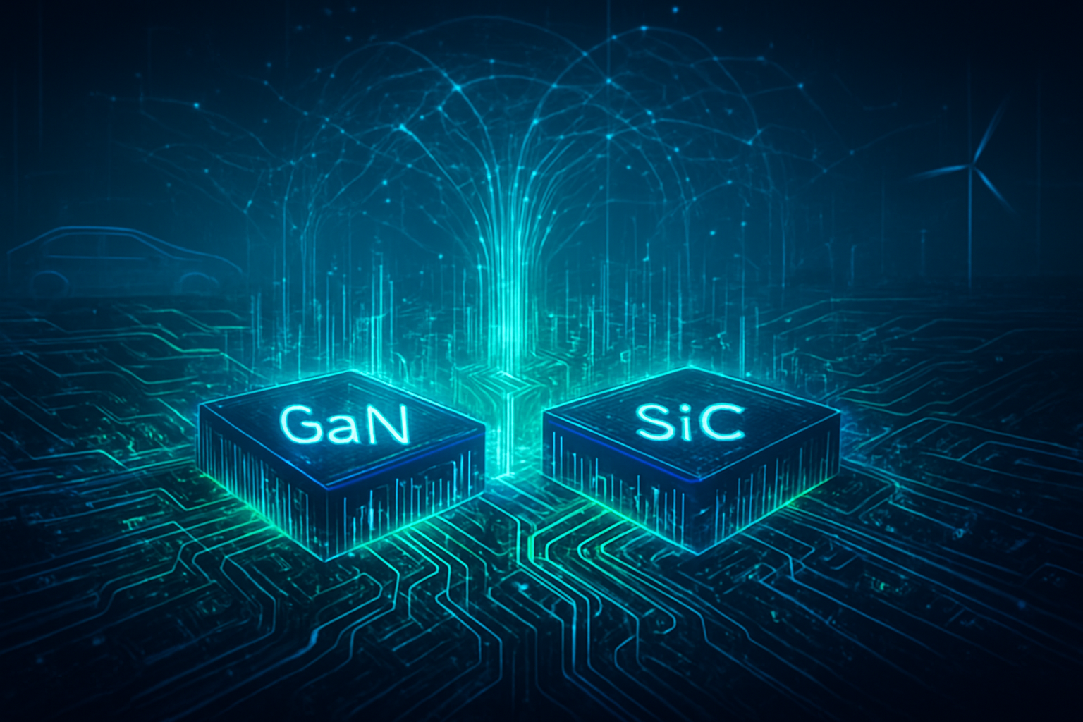
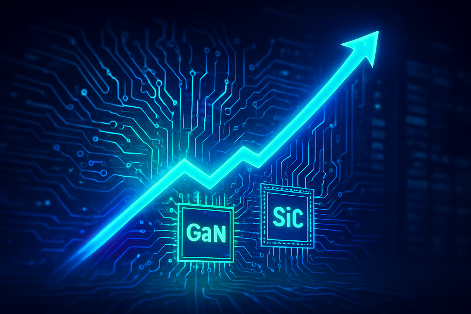
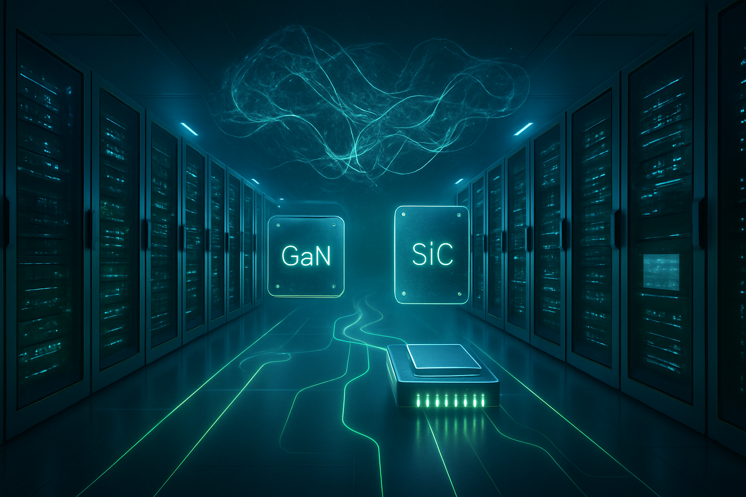
    The industry is also watching for the potential "GaN-on-SiC" (Gallium Nitride on Silicon Carbide) hybrid chips. While SiC dominates the high-voltage EV and data center market, GaN is making inroads in lower-voltage consumer applications. The ultimate "holy grail" for power electronics would be a unified architecture that utilizes Mitsubishi's trench SiC for the main power stage and GaN for the ultra-high-frequency control stages, a development that researchers believe is only a few years away.

    A New Era for High-Power AI

    In summary, Mitsubishi Electric's announcement of trench SiC-MOSFET sample shipments marks a definitive end to the "Planar Era" of power semiconductors. By achieving a 50% reduction in power loss and solving the thermal reliability issues of trench designs, Mitsubishi has provided the industry with a vital tool to manage the escalating power demands of the AI revolution and the transition to 800V electric vehicle fleets. These chips are not just incremental improvements; they are the enabling hardware for the 1MW data center rack.

    As we move through 2026, the significance of this development will be felt across the entire tech ecosystem. For AI companies, it means more compute per watt. For EV owners, it means faster charging and longer range. And for the planet, it represents a necessary step toward decoupling technological progress from exponential energy waste. Watch for the results of the initial sample evaluations in the coming months; if the 20mΩ dies perform as advertised in real-world "Rubin" GPU clusters, Mitsubishi Electric may find itself at the center of the next great hardware gold rush.


    This content is intended for informational purposes only and represents analysis of current AI developments.

    TokenRing AI delivers enterprise-grade solutions for multi-agent AI workflow orchestration, AI-powered development tools, and seamless remote collaboration platforms.
    For more information, visit https://www.tokenring.ai/.


    Published on January 16, 2026.

  • India’s Silicon Ambition: The Tata-ROHM Alliance and the Dawn of a New Semiconductor Powerhouse

    India’s Silicon Ambition: The Tata-ROHM Alliance and the Dawn of a New Semiconductor Powerhouse

    In a move that signals a seismic shift in the global technology landscape, India has officially transitioned from a chip design hub to a manufacturing contender. On December 22, 2025, just days before the dawn of 2026, Tata Electronics and ROHM Co., Ltd. (TYO:6963) announced a landmark strategic partnership to establish a domestic manufacturing framework for power semiconductors. This alliance is not merely a corporate agreement; it is a cornerstone of the 'India Semiconductor Mission' (ISM), aimed at securing a vital position in the global supply chain for electric vehicles (EVs), industrial automation, and the burgeoning AI data center market.

    The partnership focuses on the production of high-efficiency power semiconductors, specifically Silicon MOSFETs and Wide-Bandgap (WBG) materials like Silicon Carbide (SiC) and Gallium Nitride (GaN). By combining ROHM’s world-class device expertise with the industrial might of the Tata Group, the collaboration aims to address the critical shortage of "mature node" chips that have plagued global industries for years. As of January 1, 2026, the first production lines are already being prepared, marking the beginning of a new era where "Made in India" silicon will power the next generation of global infrastructure.

    Technical Mastery: From Silicon MOSFETs to Wide-Bandgap Frontiers

    The collaboration between Tata and ROHM is structured as a phased technological offensive. The immediate priority is the mass production of automotive-grade N-channel 100V, 300A Silicon MOSFETs. These components, housed in advanced Transistor Outline Leadless (TOLL) packages, are engineered for high-current applications where thermal efficiency and power density are paramount. Unlike traditional packaging, the TOLL format significantly reduces board space while enhancing heat dissipation—a critical requirement for the power management systems in modern electric drivetrains.

    Beyond standard silicon, the alliance is a major bet on Wide-Bandgap (WBG) semiconductors. As AI data centers and EVs move toward 800V architectures to handle massive power loads, traditional silicon reaches its physical limits. ROHM, a global pioneer in SiC technology, is transferring critical process knowledge to Tata to enable the localized production of SiC and GaN modules. These materials allow for higher switching frequencies and can operate at significantly higher temperatures than silicon, effectively reducing the energy footprint of AI "factories" and extending the range of EVs. This technical leap differentiates the Tata-ROHM venture from previous attempts at domestic manufacturing, which often focused on lower-value, legacy components.

    The manufacturing will be distributed across two massive hubs: the $11 billion Dholera Fab in Gujarat and the $3.2 billion Jagiroad Outsourced Semiconductor Assembly and Test (OSAT) facility in Assam. While the Dholera plant handles the complex front-end wafer fabrication, the Assam facility—slated to be fully operational by April 2026—will manage the backend assembly and testing of up to 48 million chips per day. This end-to-end integration ensures that India is not just a participant in the assembly process but a master of the entire value chain.

    Disruption in the Power Semiconductor Hierarchy

    The Tata-ROHM alliance is a direct challenge to the established dominance of European and American power semiconductor giants. Companies like Infineon Technologies AG (ETR:IFX), STMicroelectronics N.V. (NYSE:STM), and onsemi (NASDAQ:ON) now face a formidable competitor that possesses a unique "captive customer" advantage. The Tata Group’s vertical integration is its greatest weapon; Tata Motors Limited (NSE:TATAMOTORS), which controls nearly 40% of India’s EV market, provides a guaranteed high-volume demand for these chips, allowing the partnership to scale with a speed that independent manufacturers cannot match.

    Market analysts suggest that this partnership could disrupt the global pricing of SiC and GaN components. By leveraging India’s lower manufacturing costs and the massive 50% fiscal support provided by the Indian government under the ISM, Tata-ROHM can produce high-end power modules at a fraction of the cost of their Western counterparts. This "democratization" of WBG semiconductors is expected to accelerate the adoption of high-efficiency power management in mid-range industrial applications and non-luxury EVs, forcing global leaders to rethink their margin structures and supply chain strategies.

    Furthermore, the alliance serves as a pivotal implementation of the "China Plus One" strategy. Global OEMs are increasingly desperate to diversify their semiconductor sourcing away from East Asian flashpoints. By establishing a robust, high-tech manufacturing hub in India, ROHM is positioning itself as the "local" strategic architect for the Global South, using India as a launchpad to serve markets in Africa, the Middle East, and Southeast Asia.

    The Geopolitical and AI Significance of India's Rise

    The broader significance of this development cannot be overstated. We are currently witnessing the "Green AI" revolution, where the bottleneck for AI advancement is no longer just compute power, but the energy infrastructure required to sustain it. Power semiconductors are the "muscles" of the AI era, managing the electricity flow into the massive GPU clusters that drive large language models. The Tata-ROHM partnership ensures that India is not just a consumer of AI technology but a provider of the essential hardware that makes AI sustainable.

    Geopolitically, this marks India’s entry into the elite club of semiconductor-producing nations. For decades, India’s contribution to the sector was limited to high-end design services. With the Dholera and Jagiroad facilities coming online in 2026, India is effectively insulating itself from global supply shocks. This move mirrors the strategic intent of the US CHIPS Act and China’s "Made in China 2025" initiative, but with a specific focus on the high-growth power and analog sectors rather than the hyper-competitive sub-5nm logic space.

    However, the path is not without its hurdles. The industry community remains cautiously optimistic, noting that while the capital and technology are now in place, India faces a looming talent gap. Estimates suggest the country will need upwards of 300,000 specialized semiconductor professionals by 2027. The success of the Tata-ROHM venture will depend heavily on the rapid upskilling of India’s engineering workforce to handle "clean-room" manufacturing environments, a starkly different challenge from the software-centric expertise the nation is known for.

    The Road Ahead: 2026 and Beyond

    As we look toward the remainder of 2026, the first "Made in India" chips from the Tata-ROHM collaboration are expected to hit the market. In the near term, the focus will remain on stabilizing the production of Silicon MOSFETs for the domestic automotive sector. By 2027, the roadmap shifts toward trial production of SiC wafers at the Dholera fab, a move that will place India at the forefront of the global energy transition.

    Experts predict that by 2030, the Indian semiconductor market will reach a valuation of $110 billion. The Tata-ROHM partnership is the vanguard of this growth, with plans to eventually move into advanced 28nm and 40nm nodes for logic and mixed-signal chips. The ultimate challenge will be maintaining infrastructure stability—specifically the "zero-fluctuation" power and ultra-pure water supplies required for high-yield fabrication—in the face of India’s rapid industrialization.

    A New Chapter in Semiconductor History

    The Tata-ROHM alliance represents more than just a business deal; it is a declaration of industrial independence. By successfully bridging the gap between design and fabrication, India has rewritten its role in the global tech ecosystem. The key takeaways are clear: vertical integration, strategic international partnerships, and aggressive government backing have created a new powerhouse that can compete on both cost and technology.

    In the history of semiconductors, 2026 will likely be remembered as the year the "Silicon Shield" began to extend toward the Indian subcontinent. For the tech industry, the coming months will be defined by how quickly Tata can scale its Assam and Gujarat facilities. If they succeed, the global power semiconductor market will never be the same again. Investors and industry leaders should watch for the first yield reports from the Jagiroad facility in Q2 2026, as they will serve as the litmus test for India’s manufacturing future.


    This content is intended for informational purposes only and represents analysis of current AI and semiconductor developments.

    TokenRing AI delivers enterprise-grade solutions for multi-agent AI workflow orchestration, AI-powered development tools, and seamless remote collaboration platforms.
    For more information, visit https://www.tokenring.ai/.

  • Navitas Semiconductor Navigates Strategic Pivot Towards High-Growth AI and EV Markets Amidst Stock Volatility

    Navitas Semiconductor Navigates Strategic Pivot Towards High-Growth AI and EV Markets Amidst Stock Volatility

    Navitas Semiconductor (NASDAQ: NVTS), a leading innovator in gallium nitride (GaN) and silicon carbide (SiC) power semiconductors, is undergoing a significant strategic transformation, dubbed "Navitas 2.0." This pivot involves shifting focus from lower-margin consumer and mobile markets to high-power, high-growth segments like AI data centers, electric vehicles (EVs), and renewable energy infrastructure. This strategic realignment has profoundly impacted its recent market performance and stock fluctuations, with investor sentiment reflecting a cautious optimism for long-term growth despite near-term financial adjustments.

    The company's stock has shown remarkable volatility, surging 165% year-to-date in 2025, even as it faces anticipated revenue declines in the immediate future due to its deliberate exit from less profitable ventures. Navitas's immediate significance lies in its crucial role in enabling more efficient power conversion, particularly in the burgeoning AI data center market, where its GaN and SiC technologies are becoming indispensable for next-generation computing infrastructure.

    GaN and SiC: Powering the Future of High-Efficiency Electronics

    Navitas Semiconductor's core strength lies in its advanced gallium nitride (GaN) and silicon carbide (SiC) power ICs and discrete components, which are at the forefront of enabling next-generation power conversion. Unlike traditional silicon-based power semiconductors, GaN and SiC offer superior performance characteristics, including higher switching speeds, lower on-resistance, and reduced energy losses. These attributes are critical for applications demanding high power density and efficiency, such as fast chargers, data center power supplies, electric vehicle powertrains, and renewable energy inverters.

    The company's "Navitas 2.0" strategy specifically targets the deployment of these advanced materials in high-power, high-growth markets. For instance, Navitas is recognized for its GaNFast™ power ICs, which integrate GaN power FETs with drive, control, and protection features into a single, monolithic device. This integration simplifies design, reduces component count, and enhances reliability, offering a distinct advantage over discrete GaN solutions. In the SiC domain, Navitas is developing and sampling high-voltage SiC modules, including 2.3kV and 3.3kV devices, specifically for demanding applications like energy storage systems and industrial electrification.

    This approach significantly differs from previous reliance on the consumer electronics market, where profit margins are typically thinner and product lifecycles shorter. By focusing on enterprise and industrial applications, Navitas aims to leverage the inherent technical advantages of GaN and SiC to address critical pain points like power density and energy efficiency in complex systems. Initial reactions from the AI research community and power electronics industry experts have been largely positive, viewing GaN and SiC as essential technologies for the future, particularly given the escalating power demands of AI data centers. The selection of Navitas as a power semiconductor partner by NVIDIA for its next-generation 800V DC architecture in AI factory computing serves as a strong validation of Navitas's technological leadership and the market's recognition of its advanced solutions.

    Market Dynamics: Beneficiaries, Competition, and Strategic Positioning

    Navitas Semiconductor's strategic pivot towards high-power GaN and SiC solutions positions it to significantly benefit from the explosive growth in several key sectors. Companies investing heavily in AI infrastructure, electric vehicles, and renewable energy stand to gain from Navitas's ability to provide more efficient and compact power conversion. Notably, hyperscale data center operators and AI hardware manufacturers, such as NVIDIA (NASDAQ: NVDA) and other developers of AI accelerators, are direct beneficiaries, as Navitas's technology helps address the critical challenges of power delivery and thermal management in increasingly dense AI computing environments. The company's partnership with NVIDIA underscores its critical role in enabling the next generation of AI factories.

    The competitive landscape for Navitas is multifaceted, involving both established semiconductor giants and other specialized GaN/SiC players. Major tech companies like Infineon (ETR: IFX, OTCQX: IFNNY), STMicroelectronics (NYSE: STM), and Wolfspeed (NYSE: WOLF) are also heavily invested in GaN and SiC technologies. However, Navitas aims to differentiate itself through its GaNFast™ IC integration approach, offering a more complete and easy-to-implement solution compared to discrete components. This could potentially disrupt existing power supply designs that rely on more complex discrete GaN or SiC implementations. For startups in the power electronics space, Navitas's advancements could either present opportunities for collaboration or intensify competition, depending on their specific niche.

    Navitas's market positioning is strengthened by its strategic focus on specific high-growth applications where GaN and SiC offer distinct advantages. By moving away from the highly commoditized consumer mobile market, the company seeks higher-margin opportunities and more stable, long-term design wins. Its expanding ecosystem, including collaborations with GlobalFoundries (NASDAQ: GFS) for U.S.-based GaN technology and WT Microelectronics (TPE: 3036) for Asian distribution, further solidifies its strategic advantages. This network of partnerships aims to accelerate GaN adoption globally and ensure a robust supply chain, crucial for scaling its solutions in demanding enterprise and industrial markets.

    Broader Implications: Powering the AI Revolution and Beyond

    Navitas Semiconductor's advancements in GaN and SiC power semiconductors are not merely incremental improvements; they represent a fundamental shift in how power is managed in the broader AI landscape and other critical sectors. The increasing demand for computational power in AI, particularly for training large language models and running complex inference tasks, has led to a significant surge in energy consumption within data centers. Traditional silicon-based power solutions are reaching their limits in terms of efficiency and power density. GaN and SiC technologies, with their superior switching characteristics and reduced energy losses, are becoming indispensable for addressing this energy crisis, enabling smaller, lighter, and more efficient power supplies that can handle the extreme power requirements of AI accelerators.

    The impact of this shift extends far beyond data centers. In electric vehicles, GaN and SiC enable more efficient inverters and on-board chargers, leading to increased range and faster charging times. In renewable energy, they improve the efficiency of solar microinverters and energy storage systems, crucial for grid modernization and decarbonization efforts. These developments fit perfectly into broader trends of electrification, digitalization, and the pursuit of sustainability across industries.

    However, the widespread adoption of GaN and SiC also presents potential concerns. The supply chain for these relatively newer materials is still maturing compared to silicon, and any disruptions could impact production. Furthermore, the cost premium associated with GaN and SiC, while decreasing, can still be a barrier for some applications. Despite these challenges, the current trajectory suggests that GaN and SiC are on par with previous semiconductor milestones, such as the transition from germanium to silicon, in terms of their potential to unlock new levels of performance and efficiency. Their role in enabling the current AI revolution, which is heavily dependent on efficient power delivery, underscores their significance as a foundational technology for the next wave of technological innovation.

    The Road Ahead: Anticipated Developments and Challenges

    The future for Navitas Semiconductor, and indeed for the broader GaN and SiC power semiconductor market, is characterized by anticipated rapid growth and continuous innovation. In the near-term, Navitas expects to complete its strategic pivot, with management projecting Q4 2025 revenues to be the lowest point as it sheds lower-margin businesses. However, a healthier growth rate is expected to resume in late 2025 and accelerate significantly through 2027 and 2028, with substantial contributions from AI data centers and EV markets. The company's bidirectional GaN ICs, GaN BDS, launched in early 2025, are expected to ramp up in solar microinverters by late 2025, indicating new product cycles coming online.

    Long-term developments include the increasing adoption of 800-volt equipment in data centers, starting in 2026 and accelerating through 2030, which Navitas is well-positioned to capitalize on with its GaN and SiC solutions. Experts predict that the overall GaN and SiC device markets will continue robust annualized growth of 25% through 2032, highlighting the sustained demand for these efficient power technologies. Potential applications on the horizon include more advanced power solutions for robotics, industrial automation, and even future aerospace applications, where weight and efficiency are paramount.

    However, several challenges need to be addressed. Scaling manufacturing to meet the anticipated demand, further reducing the cost of GaN and SiC devices, and educating the broader engineering community on their optimal design and implementation are crucial. Competition from other wide-bandgap materials and ongoing advancements in silicon-based technologies could also pose challenges. Despite these hurdles, experts predict that the undeniable performance benefits and efficiency gains offered by GaN and SiC will drive their continued integration into critical infrastructure. What to watch for next includes Navitas's revenue rebound in 2027 and beyond, further strategic partnerships, and the expansion of its product portfolio into even higher power and voltage applications.

    Navitas's Strategic Resurgence: A New Era for Power Semiconductors

    Navitas Semiconductor's journey through 2025 and into the future marks a pivotal moment in the power semiconductor industry. The company's "Navitas 2.0" strategy, a decisive shift from low-margin consumer electronics to high-growth, high-power applications like AI data centers, EVs, and renewable energy, is a clear recognition of the evolving demands for energy efficiency and power density. While this transition has introduced near-term revenue pressures and stock volatility, the significant year-to-date stock surge of 165% reflects strong investor confidence in its long-term vision and its foundational role in powering the AI revolution.

    This development is profoundly significant in AI history, as the efficiency of power delivery is becoming as critical as computational power itself. Navitas's GaN and SiC technologies are not just components; they are enablers of the next generation of AI infrastructure, allowing for more powerful, compact, and sustainable computing. The validation from industry leaders like NVIDIA underscores the transformative potential of these materials. The challenges of scaling production, managing costs, and navigating a competitive landscape remain, but Navitas's strong cash position and strategic partnerships provide a solid foundation for continued innovation and market penetration.

    In the coming weeks and months, observers should closely watch for Navitas's Q4 2025 results as the anticipated low point in its revenue trajectory. Subsequent quarters will be crucial indicators of the success of its strategic pivot and the ramp-up of its GaN and SiC solutions in key markets. Further announcements regarding partnerships, new product introductions, and design wins in AI data centers, EVs, and renewable energy will provide insights into the company's progress and its long-term impact on the global energy and technology landscape. Navitas Semiconductor is not just riding the wave of technological change; it is actively shaping the future of efficient power.


    This content is intended for informational purposes only and represents analysis of current AI developments.

    TokenRing AI delivers enterprise-grade solutions for multi-agent AI workflow orchestration, AI-powered development tools, and seamless remote collaboration platforms.
    For more information, visit https://www.tokenring.ai/.

  • Navitas Semiconductor Soars on Nvidia Partnership, Reshaping the Power Semiconductor Landscape

    Navitas Semiconductor Soars on Nvidia Partnership, Reshaping the Power Semiconductor Landscape

    Navitas Semiconductor (NASDAQ: NVTS) has recently experienced an unprecedented surge in its stock value, driven by a pivotal strategic partnership with AI giant Nvidia (NASDAQ: NVDA). This collaboration, focused on developing cutting-edge Gallium Nitride (GaN) and Silicon Carbide (SiC) power devices for Nvidia's next-generation AI infrastructure, has ignited investor confidence and significantly repositioned Navitas within the burgeoning power semiconductor market. The dramatic stock rally, particularly following announcements in June and October 2025, underscores the critical role of advanced power management solutions in the era of escalating AI computational demands.

    The partnership with Nvidia represents a significant validation of Navitas's wide-bandgap semiconductor technology, signaling a strategic shift for the company towards higher-growth, higher-margin sectors like AI data centers, electric vehicles (EVs), and renewable energy. This move is poised to redefine efficiency standards in high-power applications, offering substantial improvements in performance, density, and cost savings for hyperscale operators. The market's enthusiastic response reflects a broader recognition of Navitas's potential to become a foundational technology provider in the rapidly evolving landscape of artificial intelligence infrastructure.

    Technical Prowess Driving the AI Revolution

    The core of Navitas Semiconductor's recent success and the Nvidia partnership lies in its proprietary Gallium Nitride (GaN) and Silicon Carbide (SiC) technologies. These wide-bandgap materials are not merely incremental improvements over traditional silicon-based power semiconductors; they represent a fundamental leap forward in power conversion efficiency and density, especially crucial for the demanding requirements of modern AI data centers.

    Specifically, Navitas's GaNFast™ power ICs integrate GaN power, drive, control, sensing, and protection functions onto a single chip. This integration enables significantly faster power delivery, higher system density, and superior energy efficiency compared to conventional silicon solutions. GaN's inherent advantages, such as higher electron mobility and lower gate capacitance, make it ideal for high-frequency, high-performance power designs. For Nvidia's 800V HVDC architecture, this translates into power supplies that are not only smaller and lighter but also dramatically more efficient, reducing wasted energy and heat generation – a critical concern in densely packed AI server racks.

    Complementing GaN, Navitas's GeneSiC™ technology addresses applications requiring higher voltages, offering robust efficiency and reliability for systems up to 6,500V. SiC's superior thermal conductivity, rugged design, and high dielectric breakdown strength make it perfectly suited for the higher-power demands of AI factory computing platforms, electric vehicle charging, and industrial power supplies. The combination of GaN and SiC allows Navitas to offer a comprehensive suite of power solutions that can cater to the diverse and extreme power requirements of Nvidia's cutting-edge AI infrastructure, which standard silicon technology struggles to meet without significant compromises in size, weight, and efficiency.

    Initial reactions from the AI research community and industry experts have been overwhelmingly positive. Many view this collaboration as a game-changer, not just for Navitas but for the entire AI industry. Experts highlight that the efficiency gains promised by Navitas's technology—up to 5% improvement and a 45% reduction in copper usage per 1MW rack—are not trivial. These improvements translate directly into massive operational cost savings for hyperscale data centers, lower carbon footprints, and the ability to pack more computational power into existing footprints, thereby accelerating the deployment and scaling of AI capabilities globally.

    Reshaping the Competitive Landscape

    The strategic partnership between Navitas Semiconductor and Nvidia carries profound implications for AI companies, tech giants, and startups across the industry. Navitas (NASDAQ: NVTS) itself stands to be a primary beneficiary, solidifying its position as a leading innovator in wide-bandgap semiconductors. The endorsement from a market leader like Nvidia (NASDAQ: NVDA) not only validates Navitas's technology but also provides a significant competitive advantage in securing future design wins and market share in the high-growth AI, EV, and energy sectors.

    For Nvidia, this partnership ensures access to state-of-the-art power solutions essential for maintaining its dominance in AI computing. As AI models grow in complexity and computational demands skyrocket, efficient power delivery becomes a bottleneck. By integrating Navitas's GaN and SiC technologies, Nvidia can offer more powerful, energy-efficient, and compact AI systems, further entrenching its lead over competitors like Advanced Micro Devices (NASDAQ: AMD) and Intel (NASDAQ: INTC) in the AI accelerator market. This collaboration enables Nvidia to push the boundaries of what's possible in AI infrastructure, directly impacting the performance and scalability of AI applications globally.

    The ripple effect extends to other power semiconductor manufacturers. Companies focused solely on traditional silicon-based power management solutions may face significant disruption. The superior performance of GaN and SiC in high-frequency and high-voltage applications creates a clear competitive gap that will be challenging to bridge without substantial investment in wide-bandbandgap technologies. This could accelerate the transition across the industry towards GaN and SiC, forcing competitors to either acquire specialized expertise or rapidly develop their own next-generation solutions. Startups innovating in power electronics may find new opportunities for collaboration or acquisition as larger players seek to catch up.

    Beyond direct competitors, hyperscale cloud providers and data center operators, such as Amazon (NASDAQ: AMZN) with AWS, Microsoft (NASDAQ: MSFT) with Azure, and Google (NASDAQ: GOOGL) with Google Cloud, stand to benefit immensely. The promise of reduced energy consumption and cooling costs, coupled with increased power density, directly addresses some of their most significant operational challenges. This strategic alignment positions Navitas and Nvidia at the forefront of a paradigm shift in data center design and efficiency, potentially setting new industry standards and influencing procurement decisions across the entire tech ecosystem.

    Broader Significance in the AI Landscape

    Navitas Semiconductor's strategic partnership with Nvidia and the subsequent stock surge are not merely isolated corporate events; they signify a crucial inflection point in the broader AI landscape. This development underscores the increasingly critical role of specialized hardware, particularly in power management, in unlocking the full potential of artificial intelligence. As AI models become larger and more complex, the energy required to train and run them escalates dramatically. Efficient power delivery is no longer a secondary consideration but a fundamental enabler for continued AI advancement.

    The adoption of GaN and SiC technologies by a leading AI innovator like Nvidia validates the long-held promise of wide-bandgap semiconductors. This fits perfectly into the overarching trend of "AI infrastructure optimization," where every component, from processors to interconnects and power supplies, is being re-evaluated and redesigned for maximum performance and efficiency. The impact is far-reaching: it addresses growing concerns about the environmental footprint of AI, offering a path towards more sustainable computing. By reducing energy waste, Navitas's technology contributes to lower operational costs for data centers, which in turn can make advanced AI more accessible and economically viable for a wider range of applications.

    Potential concerns, however, include the scalability of GaN and SiC production to meet potentially explosive demand, and the initial higher manufacturing costs compared to silicon. While Navitas is addressing supply chain strengthening through partnerships like the one with GlobalFoundries (NASDAQ: GF) for US-based GaN manufacturing (announced November 20, 2025), ensuring consistent, high-volume, and cost-effective supply will be paramount. Nevertheless, the long-term benefits in terms of efficiency and performance are expected to outweigh these initial challenges.

    This milestone can be compared to previous breakthroughs in AI hardware, such as the widespread adoption of GPUs for parallel processing or the development of specialized AI accelerators like TPUs. Just as those innovations removed computational bottlenecks, the advancement in power semiconductors is now tackling the energy bottleneck. It highlights a maturing AI industry that is optimizing not just algorithms but the entire hardware stack, moving towards a future where AI systems are not only intelligent but also inherently efficient and sustainable.

    The Road Ahead: Future Developments and Predictions

    The strategic alliance between Navitas Semiconductor and Nvidia, fueled by the superior performance of GaN and SiC power semiconductors, sets the stage for significant near-term and long-term developments in AI infrastructure. In the near term, we can expect to see the accelerated integration of Navitas's 800V HVDC power devices into Nvidia's next-generation AI factory computing platforms. This will likely lead to the rollout of more energy-efficient and higher-density AI server racks, enabling data centers to deploy more powerful AI workloads within existing or even smaller footprints. The focus will be on demonstrating tangible efficiency gains and cost reductions in real-world deployments.

    Looking further ahead, the successful deployment of GaN and SiC in AI data centers is likely to catalyze broader adoption across other high-power applications. Potential use cases on the horizon include more efficient electric vehicle charging infrastructure, enabling faster charging times and longer battery life; advanced renewable energy systems, such as solar inverters and wind turbine converters, where minimizing energy loss is critical; and industrial power supplies requiring robust, compact, and highly efficient solutions. Experts predict a continued shift away from silicon in these demanding sectors, with wide-bandgap materials becoming the de facto standard for high-performance power electronics.

    However, several challenges need to be addressed for these predictions to fully materialize. Scaling up manufacturing capacity for GaN and SiC to meet the anticipated exponential demand will be crucial. This involves not only expanding existing fabrication facilities but also developing more cost-effective production methods to bring down the unit price of these advanced semiconductors. Furthermore, the industry will need to invest in training a workforce skilled in designing, manufacturing, and deploying systems that leverage these novel materials. Standardization efforts for GaN and SiC components and modules will also be important to foster wider adoption and ease integration.

    Experts predict that the momentum generated by the Nvidia partnership will position Navitas (NASDAQ: NVTS) as a key enabler of the AI revolution, with its technology becoming indispensable for future generations of AI hardware. They foresee a future where power efficiency is as critical as processing power in determining the competitiveness of AI systems, and Navitas is currently at the forefront of this critical domain. The coming years will likely see further innovations in wide-bandgap materials, potentially leading to even greater efficiencies and new applications currently unforeseen.

    A New Era for Power Semiconductors in AI

    Navitas Semiconductor's dramatic stock surge, propelled by its strategic partnership with Nvidia, marks a significant turning point in the power semiconductor market and its indispensable role in the AI era. The key takeaway is the undeniable validation of Gallium Nitride (GaN) and Silicon Carbide (SiC) technologies as essential components for the next generation of high-performance, energy-efficient AI infrastructure. This collaboration highlights how specialized hardware innovation, particularly in power management, is crucial for overcoming the energy and density challenges posed by increasingly complex AI workloads.

    This development holds immense significance in AI history, akin to previous breakthroughs in processing and memory that unlocked new computational paradigms. It underscores a maturation of the AI industry, where optimization is extending beyond software and algorithms to the fundamental physics of power delivery. The efficiency gains offered by Navitas's wide-bandgap solutions—reduced energy consumption, lower cooling requirements, and higher power density—are not just technical achievements; they are economic imperatives and environmental responsibilities for the hyperscale data centers powering the AI revolution.

    Looking ahead, the long-term impact of this partnership is expected to be transformative. It is poised to accelerate the broader adoption of GaN and SiC across various high-power applications, from electric vehicles to renewable energy, establishing new benchmarks for performance and sustainability. The success of Navitas (NASDAQ: NVTS) in securing a foundational role in Nvidia's (NASDAQ: NVDA) AI ecosystem will likely inspire further investment and innovation in wide-bandgap technologies from competitors and startups alike.

    In the coming weeks and months, industry observers should watch for further announcements regarding the deployment of Nvidia's AI platforms incorporating Navitas's technology, as well as any updates on Navitas's manufacturing scale-up efforts and additional strategic partnerships. The performance of Navitas's stock, and indeed the broader power semiconductor market, will serve as a bellwether for the ongoing technological shift towards more efficient and sustainable high-power electronics, a shift that is now inextricably linked to the future of artificial intelligence.


    This content is intended for informational purposes only and represents analysis of current AI developments.

    TokenRing AI delivers enterprise-grade solutions for multi-agent AI workflow orchestration, AI-powered development tools, and seamless remote collaboration platforms.
    For more information, visit https://www.tokenring.ai/.

  • Navitas Unleashes GaN and SiC Power for Nvidia’s 800V AI Architecture, Revolutionizing Data Center Efficiency

    Navitas Unleashes GaN and SiC Power for Nvidia’s 800V AI Architecture, Revolutionizing Data Center Efficiency

    Sunnyvale, CA – October 14, 2025 – In a pivotal moment for the future of artificial intelligence infrastructure, Navitas Semiconductor (NASDAQ: NVTS) has announced a groundbreaking suite of power semiconductors specifically engineered to power Nvidia's (NASDAQ: NVDA) ambitious 800 VDC "AI factory" architecture. Unveiled yesterday, October 13, 2025, these advanced Gallium Nitride (GaN) and Silicon Carbide (SiC) devices are poised to deliver unprecedented energy efficiency and performance crucial for the escalating demands of next-generation AI workloads and hyperscale data centers. This development marks a significant leap in power delivery, addressing one of the most pressing challenges in scaling AI—the immense power consumption and thermal management.

    The immediate significance of Navitas's new product line cannot be overstated. By enabling Nvidia's innovative 800 VDC power distribution system, these power chips are set to dramatically reduce energy losses, improve overall system efficiency by up to 5% end-to-end, and enhance power density within AI data centers. This architectural shift is not merely an incremental upgrade; it represents a fundamental re-imagining of how power is delivered to AI accelerators, promising to unlock new levels of computational capability while simultaneously mitigating the environmental and operational costs associated with massive AI deployments. As AI models grow exponentially in complexity and size, efficient power management becomes a cornerstone for sustainable and scalable innovation.

    Technical Prowess: Powering the AI Revolution with GaN and SiC

    Navitas Semiconductor's new product portfolio is a testament to the power of wide-bandgap materials in high-performance computing. The core of this innovation lies in two distinct categories of power devices tailored for different stages of Nvidia's 800 VDC power architecture:

    Firstly, 100V GaN FETs (Gallium Nitride Field-Effect Transistors) are specifically optimized for the critical lower-voltage DC-DC stages found directly on GPU power boards. In these highly localized environments, individual AI chips can draw over 1000W of power, demanding power conversion solutions that offer ultra-high density and exceptional thermal management. Navitas's GaN FETs excel here due to their superior switching speeds and lower on-resistance compared to traditional silicon-based MOSFETs, minimizing energy loss right at the point of consumption. This allows for more compact power delivery modules, enabling higher computational density within each AI server rack.

    Secondly, for the initial high-power conversion stages that handle the immense power flow from the utility grid to the 800V DC backbone of the AI data center, Navitas is deploying a combination of 650V GaN devices and high-voltage SiC (Silicon Carbide) devices. These components are instrumental in rectifying and stepping down the incoming AC power to the 800V DC rail with minimal losses. The higher voltage handling capabilities of SiC, coupled with the high-frequency switching and efficiency of GaN, allow for significantly more efficient power conversion across the entire data center infrastructure. This multi-material approach ensures optimal performance and efficiency at every stage of power delivery.

    This approach fundamentally differs from previous generations of AI data center power delivery, which typically relied on lower voltage (e.g., 54V) DC systems or multiple AC/DC and DC/DC conversion stages. The 800 VDC architecture, facilitated by Navitas's wide-bandgap components, streamlines power conversion by reducing the number of conversion steps, thereby maximizing energy efficiency, reducing resistive losses in cabling (which are proportional to the square of the current), and enhancing overall system reliability. For example, solutions leveraging these devices have achieved power supply units (PSUs) with up to 98% efficiency, with a 4.5 kW AI GPU power supply solution demonstrating an impressive power density of 137 W/in³. Initial reactions from the AI research community and industry experts have been overwhelmingly positive, highlighting the critical need for such advancements to sustain the rapid growth of AI and acknowledging Navitas's role in enabling this crucial infrastructure.

    Market Dynamics: Reshaping the AI Hardware Landscape

    The introduction of Navitas Semiconductor's advanced power solutions for Nvidia's 800 VDC AI architecture is set to profoundly impact various players across the AI and tech industries. Nvidia (NASDAQ: NVDA) stands to be a primary beneficiary, as these power semiconductors are integral to the success and widespread adoption of its next-generation AI infrastructure. By offering a more energy-efficient and high-performance power delivery system, Nvidia can further solidify its dominance in the AI accelerator market, making its "AI factories" more attractive to hyperscalers, cloud providers, and enterprises building massive AI models. The ability to manage power effectively is a key differentiator in a market where computational power and operational costs are paramount.

    Beyond Nvidia, other companies involved in the AI supply chain, particularly those manufacturing power supplies, server racks, and data center infrastructure, stand to benefit. Original Design Manufacturers (ODMs) and Original Equipment Manufacturers (OEMs) that integrate these power solutions into their server designs will gain a competitive edge by offering more efficient and dense AI computing platforms. This development could also spur innovation among cooling solution providers, as higher power densities necessitate more sophisticated thermal management. Conversely, companies heavily invested in traditional silicon-based power management solutions might face increased pressure to adapt or risk falling behind, as the efficiency gains offered by GaN and SiC become industry standards for AI.

    The competitive implications for major AI labs and tech companies are significant. As AI models become larger and more complex, the underlying infrastructure's efficiency directly translates to faster training times, lower operational costs, and greater scalability. Companies like Google (NASDAQ: GOOGL), Microsoft (NASDAQ: MSFT), Amazon (NASDAQ: AMZN), and Meta (NASDAQ: META), all of whom operate vast AI data centers, will likely prioritize adopting systems that leverage such advanced power delivery. This could disrupt existing product roadmaps for internal AI hardware development if their current power solutions cannot match the efficiency and density offered by Nvidia's 800V architecture enabled by Navitas. The strategic advantage lies with those who can deploy and scale AI infrastructure most efficiently, making power semiconductor innovation a critical battleground in the AI arms race.

    Broader Significance: A Cornerstone for Sustainable AI Growth

    Navitas's advancements in power semiconductors for Nvidia's 800V AI architecture fit perfectly into the broader AI landscape and current trends emphasizing sustainability and efficiency. As AI adoption accelerates globally, the energy footprint of AI data centers has become a significant concern. This development directly addresses that concern by offering a path to significantly reduce power consumption and associated carbon emissions. It aligns with the industry's push towards "green AI" and more environmentally responsible computing, a trend that is gaining increasing importance among investors, regulators, and the public.

    The impact extends beyond just energy savings. The ability to achieve higher power density means that more computational power can be packed into a smaller physical footprint, leading to more efficient use of real estate within data centers. This is crucial for "AI factories" that require multi-megawatt rack densities. Furthermore, simplified power conversion stages can enhance system reliability by reducing the number of components and potential points of failure, which is vital for continuous operation of mission-critical AI applications. Potential concerns, however, might include the initial cost of migrating to new 800V infrastructure and the supply chain readiness for wide-bandgap materials, although these are typically outweighed by the long-term operational benefits.

    Comparing this to previous AI milestones, this development can be seen as foundational, akin to breakthroughs in processor architecture or high-bandwidth memory. While not a direct AI algorithm innovation, it is an enabling technology that removes a significant bottleneck for AI's continued scaling. Just as faster GPUs or more efficient memory allowed for larger models, more efficient power delivery allows for more powerful and denser AI systems to operate sustainably. It represents a critical step in building the physical infrastructure necessary for the next generation of AI, from advanced generative models to real-time autonomous systems, ensuring that the industry can continue its rapid expansion without hitting power or thermal ceilings.

    The Road Ahead: Future Developments and Predictions

    The immediate future will likely see a rapid adoption of Navitas's GaN and SiC solutions within Nvidia's ecosystem, as AI data centers begin to deploy the 800V architecture. We can expect to see more detailed performance benchmarks and case studies emerging from early adopters, showcasing the real-world efficiency gains and operational benefits. In the near term, the focus will be on optimizing these power delivery systems further, potentially integrating more intelligent power management features and even higher power densities as wide-bandgap material technology continues to mature. The push for even higher voltages and more streamlined power conversion stages will persist.

    Looking further ahead, the potential applications and use cases are vast. Beyond hyperscale AI data centers, this technology could trickle down to enterprise AI deployments, edge AI computing, and even other high-power applications requiring extreme efficiency and density, such as electric vehicle charging infrastructure and industrial power systems. The principles of high-voltage DC distribution and wide-bandgap power conversion are universally applicable wherever significant power is consumed and efficiency is paramount. Experts predict that the move to 800V and beyond, facilitated by technologies like Navitas's, will become the industry standard for high-performance computing within the next five years, rendering older, less efficient power architectures obsolete.

    However, challenges remain. The scaling of wide-bandgap material production to meet potentially massive demand will be critical. Furthermore, ensuring interoperability and standardization across different vendors within the 800V ecosystem will be important for widespread adoption. As power densities increase, advanced cooling technologies, including liquid cooling, will become even more essential, creating a co-dependent innovation cycle. Experts also anticipate a continued convergence of power management and digital control, leading to "smarter" power delivery units that can dynamically optimize efficiency based on workload demands. The race for ultimate AI efficiency is far from over, and power semiconductors are at its heart.

    A New Era of AI Efficiency: Powering the Future

    In summary, Navitas Semiconductor's introduction of specialized GaN and SiC power devices for Nvidia's 800 VDC AI architecture marks a monumental step forward in the quest for more energy-efficient and high-performance artificial intelligence. The key takeaways are the significant improvements in power conversion efficiency (up to 98% for PSUs), the enhanced power density, and the fundamental shift towards a more streamlined, high-voltage DC distribution system in AI data centers. This innovation is not just about incremental gains; it's about laying the groundwork for the sustainable scalability of AI, addressing the critical bottleneck of power consumption that has loomed over the industry.

    This development's significance in AI history is profound, positioning it as an enabling technology that will underpin the next wave of AI breakthroughs. Without such advancements in power delivery, the exponential growth of AI models and the deployment of massive "AI factories" would be severely constrained by energy costs and thermal limits. Navitas, in collaboration with Nvidia, has effectively raised the ceiling for what is possible in AI computing infrastructure.

    In the coming weeks and months, industry watchers should keenly observe the adoption rates of Nvidia's 800V architecture and Navitas's integrated solutions. We should also watch for competitive responses from other power semiconductor manufacturers and infrastructure providers, as the race for AI efficiency intensifies. The long-term impact will be a greener, more powerful, and more scalable AI ecosystem, accelerating the development and deployment of advanced AI across every sector.


    This content is intended for informational purposes only and represents analysis of current AI developments.

    TokenRing AI delivers enterprise-grade solutions for multi-agent AI workflow orchestration, AI-powered development tools, and seamless remote collaboration platforms.
    For more information, visit https://www.tokenring.ai/.

  • Navitas and Nvidia Forge Alliance: GaN Powering the AI Revolution

    Navitas and Nvidia Forge Alliance: GaN Powering the AI Revolution

    SAN JOSE, CA – October 2, 2025 – In a landmark development that promises to reshape the landscape of artificial intelligence infrastructure, Navitas Semiconductor (NASDAQ: NVTS), a leading innovator in Gallium Nitride (GaN) and Silicon Carbide (SiC) power semiconductors, announced a strategic partnership with AI computing titan Nvidia (NASDAQ: NVDA). Unveiled on May 21, 2025, this collaboration is set to revolutionize power delivery in AI data centers, enabling the next generation of high-performance computing through advanced 800V High Voltage Direct Current (HVDC) architectures. The alliance underscores a critical shift towards more efficient, compact, and sustainable power solutions, directly addressing the escalating energy demands of modern AI workloads and laying the groundwork for exascale computing.

    The partnership sees Navitas providing its cutting-edge GaNFast™ and GeneSiC™ power semiconductors to support Nvidia's 'Kyber' rack-scale systems, designed to power future GPUs such as the Rubin Ultra. This move is not merely an incremental upgrade but a fundamental re-architecture of data center power, aiming to push server rack capacities to 1-megawatt (MW) and beyond, far surpassing the limitations of traditional 54V systems. The implications are profound, promising significant improvements in energy efficiency, reduced operational costs, and a substantial boost in the scalability and reliability of the infrastructure underpinning the global AI boom.

    The Technical Backbone: GaN, SiC, and the 800V Revolution

    The core of this AI advancement lies in the strategic deployment of wide-bandgap semiconductors—Gallium Nitride (GaN) and Silicon Carbide (SiC)—within an 800V HVDC architecture. As AI models, particularly large language models (LLMs), grow in complexity and computational appetite, the power consumption of data centers has become a critical bottleneck. Nvidia's next-generation AI processors, like the Blackwell B100 and B200 chips, are anticipated to demand 1,000W or more each, pushing traditional 54V power distribution systems to their physical limits.

    Navitas' contribution includes its GaNSafe™ power ICs, which integrate control, drive, sensing, and critical protection features, offering enhanced reliability and robustness with features like sub-350ns short-circuit protection. Complementing these are GeneSiC™ Silicon Carbide MOSFETs, optimized for high-power, high-voltage applications with proprietary 'trench-assisted planar' technology that ensures superior performance and extended lifespan. These technologies, combined with Navitas' patented IntelliWeave™ digital control technique, enable Power Factor Correction (PFC) peak efficiencies of up to 99.3% and reduce power losses by 30% compared to existing solutions. Navitas has already demonstrated 8.5 kW AI data center power supplies achieving 98% efficiency and 4.5 kW platforms pushing densities over 130W/in³.

    This 800V HVDC approach fundamentally differs from previous 54V systems. Legacy 54V DC systems, while established, require bulky copper busbars to handle high currents, leading to significant I²R losses (power loss proportional to the square of the current) and physical limits around 200 kW per rack. Scaling to 1MW with 54V would demand over 200 kg of copper, an unsustainable proposition. By contrast, the 800V HVDC architecture significantly reduces current for the same power, drastically cutting I²R losses and allowing for a remarkable 45% reduction in copper wiring thickness. Furthermore, Nvidia's strategy involves converting 13.8 kV AC grid power directly to 800V HVDC at the data center perimeter using solid-state transformers, streamlining power conversion and maximizing efficiency by eliminating several intermediate AC/DC and DC/DC stages. GaN excels in high-speed, high-efficiency secondary-side DC-DC conversion, while SiC handles the higher voltages and temperatures of the initial stages.

    Initial reactions from the AI research community and industry experts have been overwhelmingly positive. The partnership is seen as a major validation of Navitas' leadership in next-generation power semiconductors. Analysts and investors have responded enthusiastically, with Navitas' stock experiencing a significant surge of over 125% post-announcement, reflecting the perceived importance of this collaboration for the future of AI infrastructure. Experts emphasize Navitas' crucial role in overcoming AI's impending "power crisis," stating that without such advancements, data centers could literally run out of power, hindering AI's exponential growth.

    Reshaping the Tech Landscape: Benefits, Disruptions, and Competitive Edge

    The Navitas-Nvidia partnership and the broader expansion of GaN collaborations are poised to significantly impact AI companies, tech giants, and startups across various sectors. The inherent advantages of GaN—higher efficiency, faster switching speeds, increased power density, and superior thermal management—are precisely what the power-hungry AI industry demands.

    Which companies stand to benefit?
    At the forefront is Navitas Semiconductor (NASDAQ: NVTS) itself, validated as a critical supplier for AI infrastructure. The Nvidia partnership alone represents a projected $2.6 billion market opportunity for Navitas by 2030, covering multiple power conversion stages. Its collaborations with GigaDevice for microcontrollers and Powerchip Semiconductor Manufacturing Corporation (PSMC) for 8-inch GaN wafer production further solidify its supply chain and ecosystem. Nvidia (NASDAQ: NVDA) gains a strategic advantage by ensuring its cutting-edge GPUs are not bottlenecked by power delivery, allowing for continuous innovation in AI hardware. Hyperscale cloud providers like Amazon (NASDAQ: AMZN), Microsoft (NASDAQ: MSFT), and Google (NASDAQ: GOOGL), which operate vast AI-driven data centers, stand to benefit immensely from the increased efficiency, reduced operational costs, and enhanced scalability offered by GaN-powered infrastructure. Beyond AI, electric vehicle (EV) manufacturers like Changan Auto, and companies in solar and energy storage, are already adopting Navitas' GaN technology for more efficient chargers, inverters, and power systems.

    Competitive implications are significant. GaN technology is challenging the long-standing dominance of traditional silicon, offering an order of magnitude improvement in performance and the potential to replace over 70% of existing architectures in various applications. While established competitors like Infineon Technologies (ETR: IFX), Wolfspeed (NYSE: WOLF), STMicroelectronics (NYSE: STM), and Power Integrations (NASDAQ: POWI) are also investing heavily in wide-bandgap semiconductors, Navitas differentiates itself with its integrated GaNFast™ ICs, which simplify design complexity for customers. The rapidly growing GaN and SiC power semiconductor market, projected to reach $23.52 billion by 2032 from $1.87 billion in 2023, signals intense competition and a dynamic landscape.

    Potential disruption to existing products or services is considerable. The transition to 800V HVDC architectures will fundamentally disrupt existing 54V data center power systems. GaN-enabled Power Supply Units (PSUs) can be up to three times smaller and achieve efficiencies over 98%, leading to a rapid shift away from larger, less efficient silicon-based power conversion solutions in servers and consumer electronics. Reduced heat generation from GaN devices will also lead to more efficient cooling systems, impacting the design and energy consumption of data center climate control. In the EV sector, GaN integration will accelerate the development of smaller, more efficient, and faster-charging power electronics, affecting current designs for onboard chargers, inverters, and motor control.

    Market positioning and strategic advantages for Navitas are bolstered by its "pure-play" focus on GaN and SiC, offering integrated solutions that simplify design. The Nvidia partnership serves as a powerful validation, securing Navitas' position as a critical supplier in the booming AI infrastructure market. Furthermore, its partnership with Powerchip for 8-inch GaN wafer production helps secure its supply chain, particularly as other major foundries scale back. This broad ecosystem expansion across AI data centers, EVs, solar, and mobile markets, combined with a robust intellectual property portfolio of over 300 patents, gives Navitas a strong competitive edge.

    Broader Significance: Powering AI's Future Sustainably

    The integration of GaN technology into critical AI infrastructure, spearheaded by the Navitas-Nvidia partnership, represents a foundational shift that extends far beyond mere component upgrades. It addresses one of the most pressing challenges facing the broader AI landscape: the insatiable demand for energy. As AI models grow exponentially, data centers are projected to consume a staggering 21% of global electricity by 2030, up from 1-2% today. GaN and SiC are not just enabling efficiency; they are enabling sustainability and scalability.

    This development fits into the broader AI trend of increasing computational intensity and the urgent need for green computing. While previous AI milestones focused on algorithmic breakthroughs – from Deep Blue to AlphaGo to the advent of large language models like ChatGPT – the significance of GaN is as a critical infrastructural enabler. It's not about what AI can do, but how AI can continue to grow and operate at scale without hitting insurmountable power and thermal barriers. GaN's ability to offer higher efficiency (over 98% for power supplies), greater power density (tripling it in some cases), and superior thermal management is directly contributing to lower operational costs, reduced carbon footprints, and optimized real estate utilization in data centers. The shift to 800V HVDC, facilitated by GaN, can reduce energy losses by 30% and copper usage by 45%, translating to thousands of megatons of CO2 savings annually by 2050.

    Potential concerns, while overshadowed by the benefits, include the high market valuation of Navitas, with some analysts suggesting that the full financial impact may take time to materialize. Cost and scalability challenges for GaN manufacturing, though addressed by partnerships like the one with Powerchip, remain ongoing efforts. Competition from other established semiconductor giants also persists. It's crucial to distinguish between Gallium Nitride (GaN) power electronics and Generative Adversarial Networks (GANs), the AI algorithm. While not directly related, the overall AI landscape faces ethical concerns such as data privacy, algorithmic bias, and security risks (like "GAN poisoning"), all of which are indirectly impacted by the need for efficient power solutions to sustain ever-larger and more complex AI systems.

    Compared to previous AI milestones, which were primarily algorithmic breakthroughs, the GaN revolution is a paradigm shift in the underlying power infrastructure. It's akin to the advent of the internet itself – a fundamental technological transformation that enables everything built upon it to function more effectively and sustainably. Without these power innovations, the exponential growth and widespread deployment of advanced AI, particularly in data centers and at the edge, would face severe bottlenecks related to energy supply, heat dissipation, and physical space. GaN is the silent enabler, the invisible force allowing AI to continue its rapid ascent.

    The Road Ahead: Future Developments and Expert Predictions

    The partnership between Navitas Semiconductor and Nvidia, along with Navitas' expanded GaN collaborations, signals a clear trajectory for future developments in AI power infrastructure and beyond. Both near-term and long-term advancements are expected to solidify GaN's position as a cornerstone technology.

    In the near-term (1-3 years), we can expect to see an accelerated rollout of GaN-based power supplies in data centers, pushing efficiencies above 98% and power densities to new highs. Navitas' plans to introduce 8-10kW power platforms by late 2024 to meet 2025 AI requirements illustrate this rapid pace. Hybrid solutions integrating GaN with SiC are also anticipated, optimizing cost and performance for diverse AI applications. The adoption of low-voltage GaN devices for 48V power distribution in data centers and consumer electronics will continue to grow, enabling smaller, more reliable, and cooler-running systems. In the electric vehicle sector, GaN is set to play a crucial role in enabling 800V EV architectures, leading to more efficient vehicles, faster charging, and lighter designs, with companies like Changan Auto already launching GaN-based onboard chargers. Consumer electronics will also benefit from smaller, faster, and more efficient GaN chargers.

    Long-term (3-5+ years), the impact will be even more profound. The Navitas-Nvidia partnership aims to enable exascale computing infrastructure, targeting a 100x increase in server rack power capacity and addressing a $2.6 billion market opportunity by 2030. Furthermore, AI itself is expected to integrate with power electronics, leading to "cognitive power electronics" capable of predictive maintenance and real-time health monitoring, potentially predicting failures days in advance. Continued advancements in 200mm GaN-on-silicon production, leveraging advanced CMOS processes, will drive down costs, increase manufacturing yields, and enhance the performance of GaN devices across various voltage ranges. The widespread adoption of 800V DC architectures will enable highly efficient, scalable power delivery for the most demanding AI workloads, ensuring greater reliability and reducing infrastructure complexity.

    Potential applications and use cases on the horizon are vast. Beyond AI data centers and cloud computing, GaN will be critical for high-performance computing (HPC) and AI clusters, where stable, high-power delivery with low latency is paramount. Its advantages will extend to electric vehicles, renewable energy systems (solar inverters, energy storage), edge AI deployments (powering autonomous vehicles, industrial IoT, smart cities), and even advanced industrial applications and home appliances.

    Challenges that need to be addressed include the ongoing efforts to further reduce the cost of GaN devices and scale up production, though partnerships like Navitas' with Powerchip are directly tackling these. Seamless integration of GaN devices with existing silicon-based systems and power delivery architectures requires careful design. Ensuring long-term reliability and robustness in demanding high-power, high-temperature environments, as well as managing thermal aspects in ultra-high-density applications, remain key design considerations. Furthermore, a limited talent pool with expertise in these specialized areas and the need for resilient supply chains are important factors for sustained growth.

    Experts predict a significant and sustained expansion of GaN's market, particularly in AI data centers and electric vehicles. Infineon Technologies anticipates GaN reaching major adoption milestones by 2025 across mobility, communication, AI data centers, and rooftop solar, with plans for hybrid GaN-SiC solutions. Alex Lidow, CEO of EPC, sees GaN making significant inroads into AI server cards' DC/DC converters, with the next logical step being the AI rack AC/DC system. He highlights multi-level GaN solutions as optimal for addressing tight form factors as power levels surge beyond 8 kW. Navitas' strategic partnerships are widely viewed as "masterstrokes" that will secure a pivotal role in powering AI's next phase. Despite the challenges, the trends of mass production scaling and maturing design processes are expected to drive down GaN prices, solidifying its position as an indispensable complement to silicon in the era of AI.

    Comprehensive Wrap-Up: A New Era for AI Power

    The partnership between Navitas Semiconductor and Nvidia, alongside Navitas' broader expansion of Gallium Nitride (GaN) collaborations, represents a watershed moment in the evolution of AI infrastructure. This development is not merely an incremental improvement but a fundamental re-architecture of how artificial intelligence is powered, moving towards vastly more efficient, compact, and scalable solutions.

    Key takeaways include the critical shift to 800V HVDC architectures, enabled by Navitas' GaN and SiC technologies, which directly addresses the escalating power demands of AI data centers. This move promises up to a 5% improvement in end-to-end power efficiency, a 45% reduction in copper wiring, and a 70% decrease in maintenance costs, all while enabling server racks to handle 1 MW of power and beyond. The collaboration validates GaN as a mature and indispensable technology for high-performance computing, with significant implications for energy sustainability and operational economics across the tech industry.

    In the grand tapestry of AI history, this development marks a crucial transition from purely algorithmic breakthroughs to foundational infrastructural advancements. While previous milestones focused on what AI could achieve, this partnership focuses on how AI can continue to scale and thrive without succumbing to power and thermal limitations. It's an assessment of this development's significance as an enabler – a "paradigm shift" in power electronics that is as vital to the future of AI as the invention of the internet was to information exchange. Without such innovations, the exponential growth of AI and its widespread deployment in data centers, autonomous vehicles, and edge computing would face severe bottlenecks.

    Final thoughts on long-term impact point to a future where AI is not only more powerful but also significantly more sustainable. The widespread adoption of GaN will contribute to a substantial reduction in global energy consumption and carbon emissions associated with computing. This partnership sets a new standard for power delivery in high-performance computing, driving innovation across the semiconductor, cloud computing, and electric vehicle industries.

    What to watch for in the coming weeks and months includes further announcements regarding the deployment timelines of 800V HVDC systems, particularly as Nvidia's next-generation GPUs come online. Keep an eye on Navitas' production scaling efforts with Powerchip, which will be crucial for meeting anticipated demand, and observe how other major semiconductor players respond to this strategic alliance. The ripple effects of this partnership are expected to accelerate GaN adoption across various sectors, making power efficiency and density a key battleground in the ongoing race for AI supremacy.

    This content is intended for informational purposes only and represents analysis of current AI developments.

    TokenRing AI delivers enterprise-grade solutions for multi-agent AI workflow orchestration, AI-powered development tools, and seamless remote collaboration platforms.
    For more information, visit https://www.tokenring.ai/.