Tag: PowerVia

  • Intel’s 1.8nm Breakthrough: The Silicon Giant Mounts a High-Stakes Comeback with AI and 18A Mastery

    Intel’s 1.8nm Breakthrough: The Silicon Giant Mounts a High-Stakes Comeback with AI and 18A Mastery

    As of February 6, 2026, the global semiconductor landscape is witnessing a seismic shift as Intel (NASDAQ: INTC) officially enters the high-volume manufacturing (HVM) phase of its ambitious 18A process node. Following a string of turbulent years, the company’s Q4 2025 earnings report, released late last month, signaled a definitive turning point. Intel beat analyst expectations with $13.7 billion in revenue, driven by a recovering data center market and the initial ramp-up of its next-generation AI processors. This financial stability, bolstered by a landmark $5 billion strategic investment from NVIDIA (NASDAQ: NVDA), suggests that Intel’s "five nodes in four years" roadmap has not only survived but is now actively reshaping the competitive dynamics of the AI era.

    The cornerstone of this resurgence is a dual-track strategy that separates Intel’s product design from its manufacturing arm, Intel Foundry. By achieving HVM status for the 18A (1.8nm-class) node, Intel has successfully leapfrogged its rivals in several key architectural transitions. At the heart of this victory is PowerVia, a revolutionary backside power delivery technology that gives Intel a technical edge in transistor efficiency. As the industry pivots toward power-hungry generative AI applications, Intel’s ability to manufacture more efficient, high-performance silicon at scale is positioning the company as the primary Western alternative to the dominant Taiwan Semiconductor Manufacturing Company (NYSE: TSM).

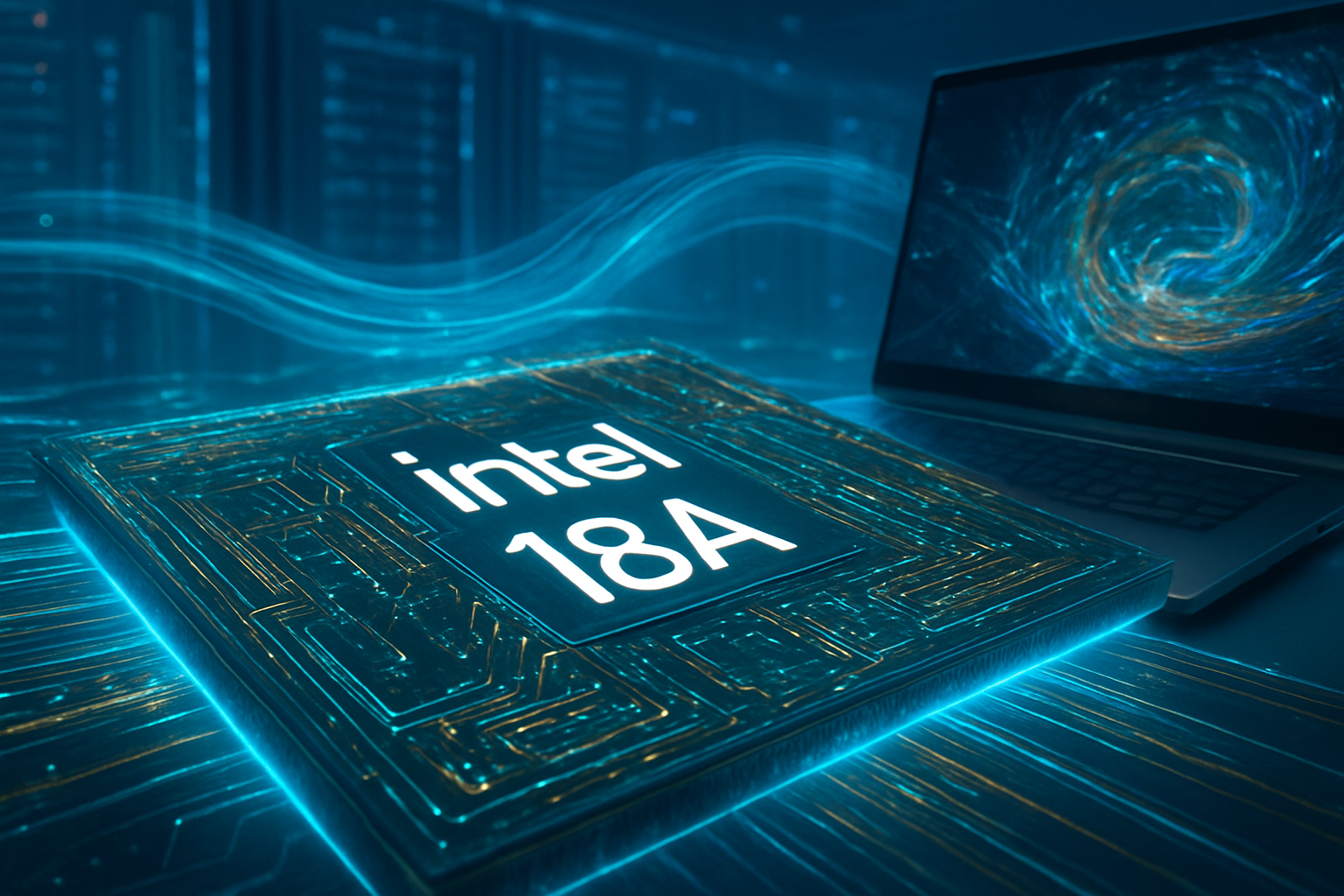
    The Engineering Triumph of 18A and PowerVia

    Intel’s 18A process node represents more than just a reduction in transistor size; it is a fundamental re-engineering of how chips are powered. The most significant advancement is PowerVia, Intel’s implementation of Backside Power Delivery (BSPDN). Traditionally, both data signals and power lines are routed through a complex web of metal layers on top of the transistors. This creates "wiring congestion" that can lead to interference and energy loss. PowerVia solves this by moving the power delivery network to the reverse side of the silicon wafer. This "cable management" at the atomic level has already demonstrated a 6% boost in clock frequency and a significant reduction in voltage drop in production silicon.

    The technical implications are profound. By separating power and data, Intel can pack transistors more densely without the thermal bottlenecks that plagued previous generations. This technology has enabled the successful launch of Panther Lake (Core Ultra Series 3) for the consumer AI PC market and Clearwater Forest (Xeon 6+) for high-density server environments. Initial yield reports for 18A are hovering between 55% and 65%—a healthy figure for a node in its first month of high-volume production. Industry experts note that Intel currently holds a 6-to-12-month lead in BSPDN technology over TSMC, whose equivalent "Super Power Rail" is not expected to reach volume production until late 2026 or 2027 with their A16 node.

    Furthermore, 18A introduces the RibbonFET gate-all-around (GAA) transistor architecture, which replaces the long-standing FinFET design. This change allows for finer control over the electrical current flowing through the transistor, further reducing leakage and boosting performance-per-watt. The combination of RibbonFET and PowerVia makes 18A the most advanced logic process ever developed on American soil, providing the technical foundation for Intel's transition from a struggling incumbent to a cutting-edge foundry service provider.

    Strategic Realignment and the NVIDIA Alliance

    Intel's success is increasingly tied to its "Foundry Independence" model. Under the leadership of CEO Lip-Bu Tan, the company has established a strict "firewall" between its manufacturing facilities and its internal product teams. This move was essential to win the trust of external customers who compete directly with Intel’s chip divisions. The strategy is already paying dividends; the 18A Process Design Kit (PDK) version 1.0 is now fully in the hands of external designers, with Microsoft (NASDAQ: MSFT) and potentially Apple (NASDAQ: AAPL) identified as early lead partners for future custom silicon.

    The most surprising development in the strategic landscape is the deepening alliance with NVIDIA. The $5 billion investment from the AI chip leader late in 2025 has created a unique "coopetition" dynamic. While Intel’s Gaudi 3 and upcoming Gaudi 4 accelerators compete with NVIDIA’s mid-range offerings, NVIDIA is increasingly looking to Intel Foundry to diversify its supply chain and reduce its over-reliance on a single geographic region for manufacturing. This partnership suggests that in the high-stakes world of AI, manufacturing capacity is the ultimate currency, and Intel is one of the few players capable of printing the "gold" that powers modern neural networks.

    However, the dual-track strategy also involves a heavy dose of pragmatism. Intel has confirmed that it will continue to use external foundries like TSMC for specific non-core components, such as GPU or I/O tiles, where it makes economic sense. This "disaggregated manufacturing" approach allows Intel to focus its internal 18A capacity on the most critical high-margin compute tiles, ensuring that factory floors in Arizona and Ohio are utilized for the most advanced technologies while maintaining a flexible supply chain.

    AI Everywhere: From the Data Center to the Desktop

    The broader significance of Intel’s 18A breakthrough lies in its "AI Everywhere" initiative. In the data center, the 18A-based Clearwater Forest chips are designed to handle the massive throughput required for large language model (LLM) inference. Meanwhile, Intel's Gaudi 3 accelerators are seeing wide deployment through partners like Dell (NYSE: DELL) and Cisco (NASDAQ: CSCO), offering a cost-effective alternative for enterprises that do not require the extreme performance of NVIDIA’s top-tier H-series or B-series Blackwell chips.

    On the consumer side, the launch of Panther Lake marks the arrival of the "Next-Gen AI PC." Featuring a Neural Processing Unit (NPU) capable of delivering over 50 TOPS (Trillions of Operations Per Second), these 18A chips allow for sophisticated on-device AI tasks—such as real-time video translation and local LLM execution—without relying on the cloud. This shift toward edge AI is critical for privacy-conscious enterprises and reflects a broader trend in the industry to move computation closer to the user to reduce latency and bandwidth costs.

    Comparatively, this milestone echoes Intel’s historic "Tick-Tock" model of the early 2010s, but with significantly higher stakes. If 18A continues to scale successfully, it will validate the U.S. government’s push for domestic semiconductor sovereignty. For the AI landscape, it means a more resilient supply chain and a return to fierce competition in transistor density, which historically has been the primary driver of the exponential gains in computing power defined by Moore's Law.

    The Road Ahead: 14A and Jaguar Shores

    Looking toward the late 2026 and 2027 horizon, Intel is already preparing its next act. The 14A node is currently in the late stages of development, with expectations that it will be the first process to utilize High-Numerical Aperture (High-NA) EUV lithography at scale. This will be essential for creating even smaller features required for the next generation of AI super-chips.

    In terms of product roadmap, all eyes are on Jaguar Shores, the successor to the Falcon Shores architecture. Jaguar Shores is expected to be a true "XPU," integrating high-performance CPU cores and specialized AI accelerator cores onto a single package using 18A technology. If successful, this could challenge the dominance of integrated solutions like NVIDIA’s Grace Hopper superchips. Additionally, the Nova Lake consumer architecture, slated for late 2026, aims to leverage the 14A node to deliver a 60% improvement in multi-threaded performance, potentially reclaiming the performance crown in the laptop and desktop markets.

    The primary challenges remaining for Intel are yield optimization and capital management. While 55-65% yields are a strong start, the company must reach the 70-80% range to achieve the margins necessary to sustain its massive R&D budget. Furthermore, Intel has pivoted to a more disciplined capital approach, slowing factory construction in Europe to focus on outfitting its domestic fabs with the necessary production equipment to alleviate lingering machine bottlenecks.

    A New Era for Intel

    Intel’s transition into a viable, leading-edge foundry for the AI era is no longer a theoretical goal—it is a production reality. The combination of the 18A node and PowerVia technology has given the company its most significant technical advantage in over a decade. By successfully navigating the "five nodes in four years" challenge, Intel has silenced many of its loudest skeptics and established a foundation for long-term growth.

    As we move through 2026, the key metrics to watch will be the acquisition of third-party foundry customers and the performance of the first 18A-based server chips in real-world workloads. If Intel can maintain its execution momentum, the 18A breakthrough will be remembered as the moment the company reclaimed its status as a pillar of the global technology ecosystem. The silicon giant is back, and it is powered by the very AI revolution it is now helping to build.


    This content is intended for informational purposes only and represents analysis of current AI developments.

    TokenRing AI delivers enterprise-grade solutions for multi-agent AI workflow orchestration, AI-powered development tools, and seamless remote collaboration platforms.
    For more information, visit https://www.tokenring.ai/.

  • Intel 18A Node Reaches High-Volume Production in Arizona

    Intel 18A Node Reaches High-Volume Production in Arizona

    In a move that signals a tectonic shift in the global semiconductor landscape, Intel (NASDAQ: INTC) has officially commenced high-volume manufacturing (HVM) of its pioneering Intel 18A process node at its Ocotillo campus in Chandler, Arizona. This milestone marks the successful completion of CEO Pat Gelsinger’s audacious "5 nodes in 4 years" (5N4Y) roadmap, a strategic sprint designed to reclaim the company's manufacturing leadership after years of falling behind its Asian competitors. The 18A node, roughly equivalent to 1.8nm-class technology, is not just a hardware milestone; it is the foundational platform for the next generation of artificial intelligence, providing the power efficiency and transistor density required for advanced neural processing units (NPUs) and massive data center deployments.

    The immediate significance of this launch lies in Intel’s "first-mover" advantage with two revolutionary technologies: RibbonFET and PowerVia. By beating rivals Taiwan Semiconductor Manufacturing Co. (NYSE: TSM) and Samsung (KRX: 005930) to the implementation of backside power delivery at scale, Intel has positioned itself as the primary alternative for AI chip designers who are increasingly constrained by the thermal and power limits of traditional silicon architectures. As of early 2026, the 18A ramp is already supporting flagship products such as "Panther Lake" for AI PCs and "Clearwater Forest" for high-density server environments, effectively signaling that the "process gap" between Intel and the world's leading foundries has been closed.

    The Technical Frontier: RibbonFET and PowerVia

    The Intel 18A node represents the most significant architectural overhaul of the transistor since the introduction of FinFET in 2011. At the heart of this advancement is RibbonFET, Intel’s proprietary implementation of Gate-All-Around (GAA) technology. Unlike the previous FinFET design, where the gate only covers three sides of the channel, RibbonFET wraps the gate entirely around the silicon channel. This provides significantly better electrical control, reducing current leakage—a critical factor as transistors shrink toward the atomic scale—and allowing for higher drive currents that translate directly into faster switching speeds.

    Equally transformative is PowerVia, Intel’s breakthrough in backside power delivery. Traditionally, power lines and signal wires are woven together on the front side of a chip, leading to "wiring congestion" that slows down performance and generates excess heat. PowerVia separates these functions, moving the entire power delivery network to the back of the silicon wafer. Initial data from the Arizona HVM lines indicates that PowerVia reduces voltage droop by up to 30% and enables a 6% boost in clock frequencies at identical power levels compared to front-side delivery. This "de-cluttering" of the wafer's front side has also enabled Intel to achieve a transistor density of approximately 238 million transistors per square millimeter (MTr/mm²).

    The industry response to these technical specifications has been one of cautious optimism turning into a full-scale endorsement. Early yield reports from the Ocotillo fabs suggest that Intel has achieved a stable yield rate between 55% and 75% for 18A, a threshold that many analysts believed would take much longer to reach. Experts in the AI research community note that the 15% performance-per-watt improvement over the previous Intel 3 node is specifically optimized for "always-on" AI workloads, where efficiency is just as critical as raw throughput.

    Disrupting the Foundry Monopoly

    The successful launch of 18A in Arizona has profound implications for the global foundry market, where TSMC (NYSE: TSM) has long enjoyed a near-monopoly on the most advanced nodes. With 18A now in high-volume production, Intel Foundry is no longer a theoretical competitor but a tangible threat. Tech giants such as Microsoft (NASDAQ: MSFT) and Amazon (NASDAQ: AMZN) have already signed on as major 18A customers, seeking to leverage Intel’s domestic manufacturing footprint to secure their AI supply chains. For Microsoft, the 18A node will likely power future iterations of its custom Maia AI accelerators, reducing its total dependence on external foundries.

    The competitive pressure is now squarely on TSMC and Samsung. While TSMC’s N2 (2nm) node boasts a slightly higher raw transistor density, it lacks backside power delivery, a feature TSMC does not plan to integrate until its A16 node in late 2026 or early 2027. This gives Intel a temporary "feature lead" that is attracting designers of high-performance AI silicon who need the thermal benefits of PowerVia today. Samsung, despite being the first to market with GAA technology at 3nm, has reportedly struggled with yields on its SF2 (2nm) node, leaving an opening for Intel to capture the "Number Two" spot in the global foundry rankings.

    Furthermore, the 18A node’s integration with Intel’s Foveros Direct 3D packaging technology allows for the stacking of compute tiles directly on top of each other with copper-to-copper bonding. This allows startups and AI labs to design modular "chiplet" architectures that combine 18A logic with cheaper, mature nodes for I/O, drastically lowering the barrier to entry for custom AI silicon. By offering both the cutting-edge node and the advanced packaging in a single "systems foundry" approach, Intel is repositioning itself as a one-stop-shop for the AI era.

    A New Era for the AI Landscape

    The arrival of 18A marks a pivotal moment in the broader AI landscape, moving the industry away from "AI software optimization" and back toward "silicon-led innovation." As large language models (LLMs) continue to grow in complexity, the hardware bottleneck has become the primary constraint for AI development. Intel 18A directly addresses this by providing the thermal headroom necessary for more aggressive NPU designs. This development fits into a larger trend of "Sovereign AI," where nations and corporations seek to control their own hardware destiny to ensure security and supply stability.

    The geopolitical significance of the Arizona production cannot be overstated. By achieving HVM of 18A on U.S. soil, Intel is fulfilling a core objective of the CHIPS and Science Act, providing a secure, leading-edge domestic supply of the chips that power critical infrastructure and defense systems. This creates a "silicon shield" for the U.S. tech industry, mitigating the risks associated with the geographic concentration of semiconductor manufacturing in East Asia.

    However, the rapid transition to 1.8nm-class technology also raises concerns regarding the environmental footprint of such advanced manufacturing. The extreme ultraviolet (EUV) lithography required for 18A is immensely energy-intensive. Intel has countered these concerns by committing to 100% renewable energy use at its Ocotillo campus by 2030, but the sheer scale of the 18A ramp-up will be a test for the company’s sustainability goals. Compared to previous milestones like the move to 10nm, the 18A launch is characterized by its focus on "performance-per-watt" rather than just "more transistors," reflecting the energy-hungry reality of modern AI.

    The Road to 14A and Beyond

    Looking ahead, the high-volume production of 18A is merely the beginning of Intel’s long-term roadmap. The company is already looking toward Intel 14A, which will introduce High-NA (Numerical Aperture) EUV lithography to further push the boundaries of miniaturization. Expected to enter risk production in late 2026 or early 2027, 14A will build upon the RibbonFET and PowerVia foundation established by 18A. In the near term, the industry will be watching the market reception of "Panther Lake" CPUs, which will serve as the first major commercial test of 18A’s performance in the hands of consumers.

    Future applications on the horizon include "Edge AI" devices that can run complex generative models locally without needing a cloud connection. The efficiency gains of 18A are expected to enable 24-hour battery life on AI-enhanced laptops and more sophisticated autonomous vehicle controllers that can process sensor data with minimal latency. Challenges remain, particularly in scaling the production of Foveros Direct packaging and managing the complex supply chain for the rare materials required for 1.8nm features, but experts predict that Intel’s successful 5N4Y execution has restored the "tick-tock" rhythm of innovation that the company was once famous for.

    Summary and Final Thoughts

    The start of high-volume production for Intel 18A in Arizona is more than just a company milestone; it is a signal that the era of uncontested dominance by a single foundry is over. By delivering on the "5 nodes in 4 years" promise, Intel has re-established its technical credibility and provided the AI industry with a powerful new toolkit. The combination of RibbonFET and PowerVia offers a glimpse into the future of semiconductor physics, where performance is derived from clever 3D architecture as much as it is from shrinking dimensions.

    As we move further into 2026, the success of 18A will be measured by its ability to win over the "hyperscalers" and maintain its yield advantage over TSMC’s upcoming 2nm offerings. For the first time in a decade, the silicon crown is up for grabs, and Intel has officially entered the ring. Investors and tech enthusiasts should watch for upcoming quarterly reports to see how 18A orders from external foundry customers are scaling, as these will be the ultimate barometer of Intel's long-term resurgence in the AI-driven economy.


    This content is intended for informational purposes only and represents analysis of current AI developments.

    TokenRing AI delivers enterprise-grade solutions for multi-agent AI workflow orchestration, AI-powered development tools, and seamless remote collaboration platforms.
    For more information, visit https://www.tokenring.ai/.

  • Intel Reclaims the Silicon Throne: 18A Enters High-Volume Production, Completing the ‘5 Nodes in 4 Years’ Odyssey

    Intel Reclaims the Silicon Throne: 18A Enters High-Volume Production, Completing the ‘5 Nodes in 4 Years’ Odyssey

    Intel (NASDAQ: INTC) has officially declared victory in its most ambitious engineering campaign to date, announcing today, January 30, 2026, that its Intel 18A process node has entered high-volume manufacturing (HVM). This milestone marks the formal completion of the company’s "5 Nodes in 4 Years" (5N4Y) roadmap, a high-stakes strategy initiated by CEO Pat Gelsinger in 2021 to restore the company to the vanguard of semiconductor manufacturing. With the commencement of HVM for the "Panther Lake" mobile processors and "Clearwater Forest" server chips, Intel has not only met its self-imposed deadline but has also effectively leapfrogged its rivals in several key architectural transitions.

    The successful ramp of 18A represents a seismic shift for the global technology sector. By reaching this stage, Intel has validated its move toward a "foundry-first" business model, aimed at challenging the dominance of Taiwan Semiconductor Manufacturing Company (NYSE: TSM). The transition is already bearing fruit, with the company securing significant design wins from hyperscale giants and defense agencies. As the industry grapples with the escalating demands of generative AI, the 18A node provides the dense, power-efficient foundation required for the next generation of neural processing units (NPUs) and massive multi-core data center architectures.

    The Technical Triumph of 18A: RibbonFET and PowerVia

    The Intel 18A node is more than just a reduction in feature size; it introduces two fundamental architectural changes that the industry has not seen in over a decade. The first is RibbonFET, Intel’s implementation of Gate-All-Around (GAA) transistor technology. Unlike the FinFET transistors used since 2011, RibbonFET wraps the gate entirely around the transistor channel on all four sides. This allows for superior electrical control, significantly reducing current leakage while enabling higher drive currents. In practical terms, 18A offers approximately a 15% improvement in performance-per-watt over the preceding Intel 3 node, allowing chips to run faster without exceeding thermal limits.

    Equally revolutionary is PowerVia, Intel's proprietary backside power delivery system. Historically, power and signal wires were layered together on top of the silicon, creating a "spaghetti" of interconnects that led to electrical interference and power loss. PowerVia moves the power delivery circuitry to the reverse side of the wafer, separating it entirely from the signal lines. This architectural shift reduces "voltage droop" (IR drop) by up to 30%, which translates directly into a 6% boost in clock frequency or a significant reduction in power consumption. By clearing the congestion on the top of the die, Intel has also managed to increase transistor density by nearly 10% compared to traditional routing methods.

    The dual-pronged launch of Panther Lake and Clearwater Forest showcases these technologies in action. Panther Lake, the new flagship for the Core Ultra Series 3, features the "Cougar Cove" performance cores and the "Darkmont" efficiency cores, alongside a third-generation Xe3 integrated GPU. Notably, it includes an NPU 5 capable of delivering over 50 TOPS (Trillions of Operations Per Second), setting a new bar for on-device AI in thin-and-light laptops. Meanwhile, Clearwater Forest targets the cloud, featuring up to 288 E-cores per socket. It utilizes 18A compute dies stacked onto Intel 3 base tiles using Foveros Direct 3D packaging, a testament to Intel's growing prowess in advanced heterogeneous integration.

    A New Competitive Reality for Foundry Giants

    The success of 18A has fundamentally altered the competitive landscape between Intel, TSMC, and Samsung (KRX: 005930). While TSMC still maintains a slight edge in raw transistor density, Intel has claimed a significant "first-mover" advantage in backside power delivery. TSMC’s equivalent technology, known as Super Power Rail, is not expected to reach high-volume production until its A16 node in late 2026. This window of technical leadership has allowed Intel to secure "whale" customers that previously relied solely on Asian foundries.

    The immediate beneficiaries are tech giants looking to reduce their dependence on a single source of supply. Microsoft (NASDAQ: MSFT) has confirmed that its next-generation Maia AI accelerators will be built on 18A, while Amazon (NASDAQ: AMZN) is utilizing the node for its custom AI fabric chips. Other confirmed partners include Ericsson for 5G infrastructure and Faraday Technology for a 64-core Arm-based SoC. Even companies like NVIDIA (NASDAQ: NVDA) and Broadcom (NASDAQ: AVGO), which have traditionally been loyal to TSMC, are reportedly in active testing phases with 18A. Though Broadcom expressed initial concerns regarding yields in 2025, Intel’s report of 55–75% yield rates in early 2026 suggests the process has matured enough to support high-volume commercial contracts.

    For the broader market, Intel’s resurgence provides a much-needed strategic alternative. The concentration of leading-edge logic manufacturing in Taiwan has long been a point of geopolitical concern. With Intel's 18A reaching maturity in its Oregon and Arizona facilities, the "silicon shield" is effectively expanding to North America. This geographic diversification is a strategic advantage for firms like Apple (NASDAQ: AAPL), which is rumored to be qualifying an enhanced 18A-P variant for its 2027 product lineup.

    Geopolitical and Historical Significance in the AI Era

    The completion of the "5 Nodes in 4 Years" plan is likely to be remembered as one of the most significant turnarounds in industrial history. It marks the end of an era where Intel was often viewed as a "stumbling giant" that had lost its way during the transition to Extreme Ultraviolet (EUV) lithography. By successfully navigating the technical hurdles of 18A, Intel has validated that Moore's Law is not dead but has simply moved into a more complex, three-dimensional phase. This milestone is comparable to the 2011 introduction of the FinFET, which sustained the industry for the last 15 years.

    Furthermore, the 18A launch is intrinsically tied to the "AI Gold Rush." As generative AI shifts from massive data centers to local "Edge AI" devices, the performance-per-watt gains of RibbonFET and PowerVia become critical. Without these architectural improvements, the power requirements for running large language models (LLMs) on mobile devices would be prohibitive. Intel’s ability to mass-produce these chips domestically also aligns with the goals of the U.S. CHIPS and Science Act, providing a secure, leading-edge manufacturing base for the U.S. Department of Defense (DoD), which is already a confirmed 18A customer through the RAMP-C program.

    However, challenges remain. The massive capital expenditure required to build these "Mega-Fabs" has put significant pressure on Intel’s margins. While the technology is a success, the financial sustainability of the foundry business depends on maintaining high utilization rates from external customers. The industry is watching closely to see if Intel can sustain this momentum without the "heroic" engineering efforts that defined the 5N4Y sprint.

    The Road Ahead: 14A and High-NA EUV

    Looking toward the future, Intel is already preparing its next major leap: the Intel 14A node. While 18A is the current state-of-the-art, 14A is being designed as the "war node" that Intel hopes will secure undisputed leadership through the end of the decade. This upcoming process will be the first to fully integrate High-NA EUV (High Numerical Aperture) lithography, utilizing the advanced ASML (NASDAQ: ASML) systems that Intel was the first in the industry to acquire.

    Near-term developments include the release of the Process Design Kit (PDK) 0.5 for 14A in early 2026, allowing designers to begin mapping out 1.4nm-class chips. We can also expect to see the introduction of PowerDirect, an evolutionary step beyond PowerVia that further optimizes power delivery. Intel has signaled a more disciplined "customer-first" approach for 14A, stating it will only expand capacity once firm commitments are signed, a move meant to appease investors worried about over-expansion.

    A Defining Moment for the Semiconductor Industry

    The successful launch of 18A and the completion of the 5N4Y roadmap represent a pivotal "mission accomplished" moment for Intel. The company has moved from a position of technical obsolescence to a position where it is defining the industry’s architectural standards for the next decade. The immediate rollout of Panther Lake and Clearwater Forest provides a tangible proof of concept that the technology is ready for prime time.

    As we look toward the rest of 2026, the key metrics to watch will be the "foundry ramp"—specifically, whether more high-volume customers like MediaTek or Apple formally commit to 18A production. The technical victory is won; the commercial victory is the next frontier. Intel has successfully rebuilt its engine while flying the plane, and for the first time in years, the company is no longer chasing the leaders of the semiconductor world—it is standing right beside them.


    This content is intended for informational purposes only and represents analysis of current AI developments.

    TokenRing AI delivers enterprise-grade solutions for multi-agent AI workflow orchestration, AI-powered development tools, and seamless remote collaboration platforms.
    For more information, visit https://www.tokenring.ai/.

  • Intel Reclaims the Silicon Throne: 18A Node Hits High-Volume Production, Ending a Five-Year Marathon

    Intel Reclaims the Silicon Throne: 18A Node Hits High-Volume Production, Ending a Five-Year Marathon

    In a historic turning point for the American semiconductor industry, Intel (NASDAQ: INTC) officially announced this month that its 18A process node has reached high-volume manufacturing (HVM) status. This milestone marks the formal completion of the company’s "five nodes in four years" (5N4Y) roadmap, a high-stakes engineering sprint initiated in 2021 that many industry skeptics once deemed impossible. As of January 30, 2026, Intel has not only met its self-imposed deadline but has also successfully transitioned its first wave of 18A-based products, including the "Panther Lake" consumer chips and "Clearwater Forest" Xeon processors, into mass production.

    The achievement is being hailed as the most significant shift in the global foundry landscape in over a decade. By reaching HVM ahead of its primary competitors' equivalent nodes, Intel has effectively closed the "process gap" that allowed rivals to dominate the high-performance computing market for years. For the first time since the mid-2010s, the Santa Clara giant can plausibly claim the lead in transistor architecture and power delivery, positioning itself as the premier domestic alternative for the world’s most demanding AI and data center workloads.

    The Engineering Trifecta: RibbonFET, PowerVia, and 18A

    The transition to Intel 18A is more than a simple shrink in transistor size; it represents a fundamental overhaul of how semiconductors are built. Central to this leap are two foundational technologies: RibbonFET and PowerVia. RibbonFET is Intel’s implementation of a Gate-All-Around (GAA) transistor architecture, which replaces the long-standing FinFET design. By surrounding the transistor channel on all four sides, RibbonFET provides superior control over electrical leakage and higher drive currents, resulting in a 15% improvement in performance-per-watt over the previous Intel 3 node. This enables chips to run faster while consuming less power—a critical requirement for the energy-hungry AI era.

    Equally transformative is PowerVia, Intel’s proprietary backside power delivery system. Traditionally, power and signal lines are bundled together on the front of a wafer, leading to "wiring congestion" that limits performance. PowerVia moves the power delivery to the back of the silicon, effectively separating it from the signal lines. Technical data from the initial 18A ramp at Fab 52 indicates a staggering 30% reduction in voltage droop and a 6% boost in clock frequencies at identical power levels. This "de-cluttering" of the chip’s front side allows for much higher transistor density—approximately 238 million transistors per square millimeter—setting a new benchmark for computational efficiency.

    The industry response to these technical specs has been overwhelmingly positive. Analysts at major firms have noted that while TSMC (NYSE: TSM) remains a formidable rival with its N2 node, Intel currently holds a nearly one-year lead in the implementation of backside power delivery. This "architectural head start" has allowed Intel to achieve yield stabilities exceeding 60% in early 2026, a figure that is more than sufficient for the commercial viability of high-end server and consumer silicon. Experts suggest that the combination of GAA and PowerVia on a single node has finally broken the thermal and power bottlenecks that had begun to stall Moore’s Law.

    A Shift in the Foundry Power Dynamic

    The arrival of 18A at HVM status has sent ripples through the corporate strategies of the world’s largest technology firms. For years, companies like Apple (NASDAQ: AAPL), NVIDIA (NASDAQ: NVDA), and Microsoft (NASDAQ: MSFT) have been almost entirely dependent on TSMC for their cutting-edge silicon. However, the successful 18A ramp has catalyzed a shift toward a multi-source strategy. In a landmark development for 2026, reports indicate that Apple has qualified Intel 18A-P for its entry-level M-series chips, marking the first time the iPhone maker has utilized Intel’s foundries for its custom silicon.

    Microsoft and Amazon (NASDAQ: AMZN) have also deepened their commitment to Intel Foundry. Microsoft, which had already announced its intention to use 18A for its custom AI accelerators and Maieutic processors, has reportedly expanded its order volume to include next-generation cloud infrastructure chips. This diversification is seen as a strategic necessity, reducing the "geographic risk" associated with the heavy concentration of advanced chip manufacturing in Taiwan. For Intel, these high-profile customer wins provide the massive capital inflows needed to sustain its multi-billion dollar domestic expansion.

    The competitive implications for TSMC and Samsung (KRX: 005930) are stark. While TSMC’s N2 node is expected to offer slightly higher transistor density when it reaches full volume later this year, Intel’s early lead in backside power delivery gives its customers a performance "sweet spot" that is currently unmatched. Samsung, despite being the first to introduce GAA at 3nm, has struggled to match the yield stability of Intel’s 18A. This has allowed Intel to position itself as the "premium, reliable choice" for North American and European tech giants looking to secure their supply chains against geopolitical instability.

    Re-Shoring the Future: The Significance of Fab 52

    The location of this production is as significant as the technology itself. The 18A node is being manufactured at Intel’s Fab 52 in Ocotillo, Arizona. As of early 2026, Fab 52 is the most advanced semiconductor manufacturing facility on U.S. soil, representing a massive win for the U.S. government’s efforts to re-shore critical technology via the CHIPS and Science Act. With a design capacity of 40,000 wafer starts per month, Fab 52 is not just a pilot plant but a massive industrial engine capable of satisfying a significant portion of the global demand for advanced AI chips.

    This development aligns with the growing global trend of "Sovereign AI," where nations seek to build and control their own AI infrastructure. By having 18A production based in Arizona, the United States has secured a domestic source of the world’s most advanced computing power. This reduces the risk of supply chain disruptions caused by trade conflicts or regional instability. Furthermore, it creates a high-tech ecosystem that attracts engineering talent and secondary suppliers, reinforcing the "Silicon Desert" as a primary global hub for hardware innovation.

    However, the rapid advancement of 18A also brings new challenges. The environmental impact of such massive manufacturing operations remains a point of concern, with Intel investing heavily in water reclamation and renewable energy to offset the carbon footprint of Fab 52. Additionally, the sheer complexity of 18A manufacturing requires a highly specialized workforce, putting pressure on educational institutions to produce the next generation of lithography and materials science experts at a faster rate than ever before.

    Beyond 18A: The Roadmap to 14A and Angstrom Era

    Intel is not resting on the laurels of 18A. Even as Fab 52 ramps to full capacity, the company is already looking toward its next major milestone: the 14A node. Expected to enter risk production in 2027, 14A will be the first node to utilize "High-NA" (High Numerical Aperture) EUV lithography at scale. This next-generation equipment, provided by ASML (NASDAQ: ASML), will allow Intel to print even finer features, pushing transistor density even higher and ensuring that the momentum gained with 18A is not lost in the coming years.

    The future of AI hardware will likely be defined by "system-level" integration. Under the leadership of CEO Lip-Bu Tan, who took the helm in 2025, Intel is shifting its focus toward "Intel Foundry" as a standalone service that offers not just wafers, but advanced packaging solutions like Foveros and EMIB. This allows customers to mix and match chiplets from different nodes and even different foundries, creating highly customized AI "systems-on-a-package" that were previously impossible to manufacture efficiently.

    Analysts predict that the next 24 months will see a surge in specialized AI hardware developed specifically for 18A. From edge devices that can run massive language models locally to data center GPUs that operate with 40% better efficiency, the 18A node is the foundation upon which the next era of AI will be built. The primary challenge moving forward will be maintaining this execution pace while managing the astronomical costs associated with 14A and beyond.

    A New Era for Intel and the Industry

    The successful high-volume launch of 18A in January 2026 is a watershed moment. It proves that Intel’s radical transformation into a "foundry-first" company was not just corporate rhetoric, but a viable path to survival and leadership. By hitting the 5N4Y goal, Intel has regained the trust of both Wall Street and the engineering community, demonstrating that it can execute on complex roadmaps with precision and scale.

    The significance of this development in AI history cannot be overstated. We are moving out of an era of chip scarcity and entering an era of architectural innovation. As 18A chips begin to populate the world’s data centers and consumer devices over the coming months, the impact on AI performance, energy efficiency, and sovereign security will become increasingly apparent.

    Watch for the first public benchmarks of Panther Lake in the second quarter of 2026, as well as further announcements regarding major foundry customers during the upcoming spring earnings calls. The semiconductor crown has returned to American soil, and the race for the Angstrom era has officially begun.


    This content is intended for informational purposes only and represents analysis of current AI developments.

    TokenRing AI delivers enterprise-grade solutions for multi-agent AI workflow orchestration, AI-powered development tools, and seamless remote collaboration platforms.
    For more information, visit https://www.tokenring.ai/.

  • Intel Reclaims Silicon Crown: 18A Process Hits High-Volume Production as ‘PowerVia’ Reshapes the AI Landscape

    Intel Reclaims Silicon Crown: 18A Process Hits High-Volume Production as ‘PowerVia’ Reshapes the AI Landscape

    As of January 27, 2026, the global semiconductor hierarchy has undergone its most significant shift in a decade. Intel Corporation (NASDAQ:INTC) has officially announced that its 18A (1.8nm-class) manufacturing node has reached high-volume manufacturing (HVM) status, signaling the successful completion of its "five nodes in four years" roadmap. This milestone is not just a technical victory for Intel; it marks the company’s return to the pinnacle of process leadership, a position it had ceded to competitors during the late 2010s.

    The arrival of Intel 18A represents a critical turning point for the artificial intelligence industry. By integrating the revolutionary RibbonFET gate-all-around (GAA) architecture with its industry-leading PowerVia backside power delivery technology, Intel has delivered a platform optimized for the next generation of generative AI and high-performance computing (HPC). With early silicon already shipping to lead customers, the 18A node is proving to be the "holy grail" for AI developers seeking maximum performance-per-watt in an era of skyrocketing energy demands.

    The Architecture of Leadership: RibbonFET and the PowerVia Advantage

    At the heart of Intel 18A are two foundational innovations that differentiate it from the FinFET-based nodes of the past. The first is RibbonFET, Intel’s implementation of a Gate-All-Around (GAA) transistor. Unlike the previous FinFET design, which used a vertical fin to control current, RibbonFET surrounds the transistor channel on all four sides. This allows for superior control over electrical leakage and significantly faster switching speeds. The 18A node refines the initial RibbonFET design introduced in the 20A node, resulting in a 10-15% speed boost at the same power levels compared to the already impressive 20A projections.

    The second, and perhaps more consequential breakthrough, is PowerVia—Intel’s implementation of Backside Power Delivery (BSPDN). Traditionally, power and signal wires are bundled together on the "front" of the silicon wafer, leading to "routing congestion" and voltage droop. PowerVia moves the power delivery network to the backside of the wafer, using nano-TSVs (Through-Silicon Vias) to connect directly to the transistors. This decoupling of power and signal allows for much thicker, more efficient power traces, reducing resistance and reclaiming nearly 10% of previously wasted "dark silicon" area.

    While competitors like TSMC (NYSE:TSM) have announced their own version of this technology—marketed as "Superpower Rail" for their upcoming A16 node—Intel has successfully brought its version to market nearly a year ahead of the competition. This "first-mover" advantage in backside power delivery is a primary reason for the 18A node's high performance. Industry analysts have noted that the 18A node offers a 25% performance-per-watt improvement over the Intel 3 node, a leap that effectively resets the competitive clock for the foundry industry.

    Shifting the Foundry Balance: Microsoft, Apple, and the Race for AI Supremacy

    The successful ramp of 18A has sent shockwaves through the tech giant ecosystem. Intel Foundry has already secured a backlog exceeding $20 billion, with Microsoft (NASDAQ:MSFT) emerging as a flagship customer. Microsoft is utilizing the 18A-P (Performance-enhanced) variant to manufacture its next-generation "Maia 2" AI accelerators. By leveraging Intel's domestic manufacturing capabilities in Arizona and Ohio, Microsoft is not only gaining a performance edge but also securing its supply chain against geopolitical volatility in East Asia.

    The competitive implications extend to the highest levels of the consumer electronics market. Reports from late 2025 indicate that Apple (NASDAQ:AAPL) has moved a portion of its silicon production for entry-level devices to Intel’s 18A-P node. This marks a historic diversification for Apple, which has historically relied almost exclusively on TSMC for its A-series and M-series chips. For Intel, winning an "Apple-sized" contract validates the maturity of its 18A process and proves it can meet the stringent yield and quality requirements of the world’s most demanding hardware company.

    For AI hardware startups and established giants like NVIDIA (NASDAQ:NVDA), the availability of 18A provides a vital alternative in a supply-constrained market. While NVIDIA remains a primary partner for TSMC, the introduction of Intel’s 18A-PT—a variant optimized for advanced multi-die "System-on-Chip" (SoC) designs—offers a compelling path for future Blackwell successors. The ability to stack high-performance 18A logic tiles using Intel’s Foveros Direct 3D packaging technology is becoming a key differentiator in the race to build the first 100-trillion parameter AI models.

    Geopolitics and the Reshoring of the Silicon Frontier

    Beyond the technical specifications, Intel 18A is a cornerstone of the broader geopolitical effort to reshore semiconductor manufacturing to the United States. Supported by funding from the CHIPS and Science Act, Intel’s expansion of Fab 52 in Arizona has become a symbol of American industrial renewal. The 18A node is the first advanced process in over a decade to be pioneered and mass-produced on U.S. soil before any other region, a fact that has significant implications for national security and technological sovereignty.

    The success of 18A also serves as a validation of the "Five Nodes in Four Years" strategy championed by Intel’s leadership. By maintaining an aggressive cadence, Intel has leapfrogged the standard industry cycle, forcing competitors to accelerate their own roadmaps. This rapid iteration has been essential for the AI landscape, where the demand for compute is doubling every few months. Without the efficiency gains provided by technologies like PowerVia and RibbonFET, the energy costs of maintaining massive AI data centers would likely become unsustainable.

    However, the transition has not been without concerns. The immense capital expenditure required to maintain this pace has pressured Intel’s margins, and the complexity of 18A manufacturing requires a highly specialized workforce. Critics initially doubted Intel's ability to achieve commercial yields (currently estimated at a healthy 65-75%), but the successful launch of the "Panther Lake" consumer CPUs and "Clearwater Forest" Xeon processors has largely silenced the skeptics.

    The Road to 14A and the Era of High-NA EUV

    Looking ahead, the 18A node is just the beginning of Intel’s "Angstrom-era" roadmap. The company has already begun sampling its next-generation 14A node, which will be the first in the industry to utilize High-Numerical Aperture (High-NA) Extreme Ultraviolet (EUV) lithography tools from ASML (NASDAQ:ASML). While 18A solidified Intel's recovery, 14A is intended to extend that lead, targeting another 15% performance improvement and a further reduction in feature sizes.

    The integration of 18A technology into the "Nova Lake" architecture—scheduled for late 2026—will be the next major milestone for the consumer market. Experts predict that Nova Lake will redefine the desktop and mobile computing experience by offering over 50 TOPS of NPU (Neural Processing Unit) performance, effectively making every 18A-powered PC a localized AI powerhouse. The challenge for Intel will be maintaining this momentum while simultaneously scaling its foundry services to accommodate a diverse range of third-party designs.

    A New Chapter for the Semiconductor Industry

    The high-volume manufacturing of Intel 18A marks one of the most remarkable corporate turnarounds in recent history. By delivering 10-15% speed gains and pioneering backside power delivery via PowerVia, Intel has not only caught up to the leading edge but has actively set the pace for the rest of the decade. This development ensures that the AI revolution will have the "silicon fuel" it needs to continue its exponential growth.

    As we move further into 2026, the industry's eyes will be on the retail performance of the first 18A devices and the continued expansion of Intel Foundry's customer list. The "Angstrom Race" is far from over, but with 18A now in production, Intel has firmly re-established itself as a titan of the silicon world. For the first time in a generation, the fastest and most efficient transistors on the planet are being made by the company that started it all.


    This content is intended for informational purposes only and represents analysis of current AI developments.

    TokenRing AI delivers enterprise-grade solutions for multi-agent AI workflow orchestration, AI-powered development tools, and seamless remote collaboration platforms.
    For more information, visit https://www.tokenring.ai/.

  • Intel’s 18A Turning Point: Reclaiming the Process Leadership Crown

    Intel’s 18A Turning Point: Reclaiming the Process Leadership Crown

    As of January 26, 2026, the semiconductor landscape has reached a historic inflection point that many industry veterans once thought impossible. Intel Corp (NASDAQ:INTC) has officially entered high-volume manufacturing (HVM) for its 18A (1.8nm) process node, successfully completing its ambitious "five nodes in four years" roadmap. This milestone marks the first time in over a decade that the American chipmaker has successfully wrested the technical innovation lead away from its rivals, positioning itself as a dominant force in the high-stakes world of AI silicon and foundry services.

    The significance of 18A extends far beyond a simple increase in transistor density. It represents a fundamental architectural shift in how microchips are built, introducing two "holy grail" technologies: RibbonFET and PowerVia. By being the first to bring these advancements to the mass market, Intel has secured multi-billion dollar manufacturing contracts from tech giants like Microsoft (NASDAQ:MSFT) and Amazon (NASDAQ:AMZN), signaling a major shift in the global supply chain. For the first time in the 2020s, the "Intel Foundry" vision is not just a strategic plan—it is a tangible reality that is forcing competitors to rethink their multi-year strategies.

    The Technical Edge: RibbonFET and the PowerVia Revolution

    At the heart of the 18A node are two breakthrough technologies that redefine chip performance. The first is RibbonFET, Intel’s implementation of a Gate-All-Around (GAA) transistor. Unlike the older FinFET architecture, which dominated the industry for years, RibbonFET surrounds the transistor channel on all four sides. This allows for significantly higher drive currents and vastly improved leakage control, which is essential as transistors approach the atomic scale. While Samsung Electronics (KRX:005930) was technically first to GAA at 3nm, Intel’s 18A implementation in early 2026 is being praised by the research community for its superior scalability and yield stability, currently estimated between 60% and 75%.

    However, the true "secret sauce" of 18A is PowerVia, Intel’s proprietary version of backside power delivery. Traditionally, power and data signals have shared the same "front" side of a wafer, leading to a crowded "wiring forest" that causes electrical interference and voltage droop. PowerVia moves the power delivery network to the back of the wafer, using "Nano-TSVs" (Through-Silicon Vias) to tunnel power directly to the transistors. This decoupling of power and data lines has led to a documented 30% reduction in voltage droop and a 6% boost in clock frequencies at the same power level. Initial reactions from industry experts at TechInsights suggest that this architectural shift gives Intel a definitive "performance-per-watt" advantage over current 2nm offerings from competitors.

    This technical lead is particularly evident when comparing 18A to the current offerings from Taiwan Semiconductor Manufacturing Company (NYSE:TSM). While TSMC’s N2 (2nm) node is currently in high-volume production and holds a slight lead in raw transistor density (roughly 313 million transistors per square millimeter compared to Intel’s 238 million), it lacks backside power delivery. TSMC’s equivalent technology, "Super PowerRail," is not slated for volume production until the second half of 2026 with its A16 node. This window of exclusivity allows Intel to market itself as the most efficient option for the power-hungry demands of generative AI and hyperscale data centers for the duration of early 2026.

    A New Era for Intel Foundry Services

    The success of the 18A node has fundamentally altered the competitive dynamics of the foundry market. Intel Foundry Services (IFS) has secured a massive $15 billion contract from Microsoft to produce custom AI accelerators, a move that would have been unthinkable five years ago. Furthermore, Amazon’s AWS has deepened its partnership with Intel, utilizing 18A for its next-generation Xeon 6 fabric silicon. Even Apple (NASDAQ:AAPL), which has long been the crown jewel of TSMC’s client list, has reportedly signed on for the performance-enhanced 18A-P variant to manufacture entry-level M-series chips for its 2027 device lineup.

    The strategic advantage for these tech giants is twofold: performance and geopolitical resilience. By utilizing Intel’s domestic manufacturing sites, such as Fab 52 in Arizona and the modernized facilities in Oregon, US-based companies are mitigating the risks associated with the concentrated supply chain in East Asia. This has been bolstered by the U.S. government’s $3 billion "Secure Enclave" contract, which tasks Intel with producing the next generation of sensitive defense and intelligence chips. The availability of 18A has transformed Intel from a struggling integrated device manufacturer into a critical national asset and a viable alternative to the TSMC monopoly.

    The competitive pressure is also being felt by NVIDIA (NASDAQ:NVDA). While the AI GPU leader continues to rely on TSMC for its flagship H-series and B-series chips, it has invested $5 billion into Intel’s advanced packaging ecosystem, specifically Foveros and EMIB. Experts believe this is a precursor to NVIDIA moving some of its mid-range production to Intel 18A by late 2026 to ensure supply chain diversity. This market positioning has allowed Intel to maintain a premium pricing strategy for 18A wafers, even as it works to improve the "golden yield" threshold toward 80%.

    Wider Significance: The Geopolitics of Silicon

    The 18A milestone is a significant chapter in the broader history of computing, marking the end of the "efficiency plateau" that plagued the industry in the early 2020s. As AI models grow exponentially in complexity, the demand for energy-efficient silicon has become the primary constraint on global AI progress. By successfully implementing backside power delivery before its peers, Intel has effectively moved the goalposts for what is possible in data center density. This achievement fits into a broader trend of "Angstrom-era" computing, where breakthroughs are no longer just about smaller transistors, but about smarter ways to power and cool them.

    From a global perspective, the success of 18A represents a major victory for the U.S. CHIPS Act and Western efforts to re-shore semiconductor manufacturing. For the first time in two decades, a leading-edge process node is being ramped in the United States concurrently with, or ahead of, its Asian counterparts. This has significant implications for global stability, reducing the world's reliance on the Taiwan Strait for the highest-performance silicon. However, this shift has also sparked concerns regarding the immense energy and water requirements of these new "Angstrom-scale" fabs, prompting calls for more sustainable manufacturing practices in the desert regions of the American Southwest.

    Comparatively, the 18A breakthrough is being viewed as similar in impact to the introduction of High-K Metal Gate in 2007 or the transition to FinFET in 2011. It is a fundamental change in the "physics of the chip" that will dictate the design rules for the next decade. While TSMC remains the yield and volume king, Intel’s 18A has shattered the aura of invincibility that surrounded the Taiwanese firm, proving that a legacy giant can indeed pivot and innovate under the right leadership—currently led by CEO Lip-Bu Tan.

    Future Horizons: Toward 14A and High-NA EUV

    Looking ahead, the road doesn't end at 18A. Intel is already aggressively pivoting its R&D teams toward the 14A (1.4nm) node, which is scheduled for risk production in late 2027. This next step will be the first to fully utilize "High-NA" (High Numerical Aperture) Extreme Ultraviolet (EUV) lithography. These massive, $380 million machines from ASML are already being calibrated in Intel’s Oregon facilities. The 14A node is expected to offer a further 15% performance-per-watt improvement and will likely see the first implementation of stacked transistors (CFETs) toward the end of the decade.

    The immediate next step for 18A is the retail launch of "Panther Lake," the Core Ultra Series 3 processors, which hit global shelves tomorrow, January 27, 2026. These chips will be the first 18A products available to consumers, featuring a dedicated NPU (Neural Processing Unit) capable of 100+ TOPS (Trillions of Operations Per Second), setting a new bar for AI PCs. Challenges remain, however, particularly in the scaling of advanced packaging. As chips become more complex, the "bottleneck" is shifting from the transistor to the way these tiny tiles are bonded together. Intel will need to significantly expand its packaging capacity in New Mexico and Malaysia to meet the projected 18A demand.

    A Comprehensive Wrap-Up: The New Leader?

    The arrival of Intel 18A in high-volume manufacturing is a watershed moment for the technology industry. By successfully delivering PowerVia and RibbonFET ahead of the competition, Intel has reclaimed its seat at the table of technical leadership. While the company still faces financial volatility—highlighted by recent stock fluctuations following conservative Q1 2026 guidance—the underlying engineering success of 18A provides a solid foundation that was missing for nearly a decade.

    The key takeaway for 2026 is that the semiconductor race is no longer a one-horse race. The rivalry between Intel, TSMC, and Samsung has entered its most competitive phase yet, with each player holding a different piece of the puzzle: TSMC with its unmatched yields and density, Samsung with its GAA experience, and Intel with its first-mover advantage in backside power. In the coming months, all eyes will be on the retail performance of Panther Lake and the first benchmarks of the 18A-based Xeon "Clearwater Forest" server chips. If these products meet their ambitious performance targets, the "Process Leadership Crown" may stay in Santa Clara for a very long time.


    This content is intended for informational purposes only and represents analysis of current AI and semiconductor developments as of January 26, 2026.

    TokenRing AI delivers enterprise-grade solutions for multi-agent AI workflow orchestration, AI-powered development tools, and seamless remote collaboration platforms.
    For more information, visit https://www.tokenring.ai/.

  • The Angstrom Era Arrives: Intel 18A Hits High-Volume Production as Backside Power Redefines Silicon Efficiency

    The Angstrom Era Arrives: Intel 18A Hits High-Volume Production as Backside Power Redefines Silicon Efficiency

    As of January 20, 2026, the global semiconductor landscape has shifted on its axis. Intel (Nasdaq:INTC) has officially announced that its 18A process node—the cornerstone of its "five nodes in four years" strategy—has entered high-volume manufacturing (HVM). This milestone marks the first time in nearly a decade that the American chipmaker has reclaimed a leadership position in transistor architecture and power delivery, moving ahead of its primary rivals, TSMC (NYSE:TSM) and Samsung (KRX:005930), in the implementation of backside power delivery.

    The significance of 18A reaching maturity cannot be overstated. By successfully scaling PowerVia—Intel's proprietary backside power delivery network (BSPDN)—the company has decoupled power delivery from signal routing, effectively solving one of the most persistent bottlenecks in modern chip design. This breakthrough isn't just a technical win; it is an industrial pivot that positions Intel as the premier foundry for the next generation of generative AI accelerators and high-performance computing (HPC) processors, attracting early commitments from heavyweights like Microsoft (Nasdaq:MSFT) and Amazon (Nasdaq:AMZN).

    The 18A node's success is built on two primary pillars: RibbonFET (Gate-All-Around) transistors and PowerVia. While competitors are still refining their own backside power solutions, Intel’s PowerVia is already delivering tangible gains in the first wave of 18A products, including the "Panther Lake" consumer chips and "Clearwater Forest" Xeon processors. By moving the "plumbing" of the chip—the power wires—to the back of the wafer, Intel has reduced voltage droop (IR drop) by a staggering 30%. This allows transistors to receive a more consistent electrical current, translating to a 6% to 10% increase in clock frequencies at the same power levels compared to traditional designs.

    Technically, PowerVia works by thinning the silicon wafer to a fraction of its original thickness to expose the transistor's bottom side. The power delivery network is then fabricated on this reverse side, utilizing Nano-TSVs (Through-Silicon Vias) to connect directly to the transistor's contact level. This departure from the decades-old method of routing both power and signals through a complex web of metal layers on the front side has allowed for over 90% cell utilization. In practical terms, this means Intel can pack more transistors into a smaller area without the massive signal congestion that typically plagues sub-2nm nodes.

    Initial feedback from the semiconductor research community has been overwhelmingly positive. Experts at the IMEC research hub have noted that Intel’s early adoption of backside power has given them a roughly 12-to-18-month lead in solving the "power-signal conflict." In previous nodes, power and signal lines would often interfere with one another, causing electromagnetic crosstalk and limiting the maximum frequency of the processor. By physically separating these layers, Intel has effectively "cleaned" the signal environment, allowing for cleaner data transmission and higher efficiency.

    This development has immediate and profound implications for the AI industry. High-performance AI training chips, which consume massive amounts of power and generate intense heat, stand to benefit the most from the 18A node. The improved thermal path created by thinning the wafer for PowerVia brings the transistors closer to cooling solutions, a critical advantage for data center operators trying to manage the thermal loads of thousands of interconnected GPUs and TPUs.

    Major tech giants are already voting with their wallets. Microsoft (Nasdaq:MSFT) has reportedly deepened its partnership with Intel Foundry, securing 18A capacity for its custom-designed Maiai AI accelerators. For companies like Apple (Nasdaq:AAPL), which has traditionally relied almost exclusively on TSMC, the stability and performance of Intel 18A present a viable alternative that could diversify their supply chains. This shift introduces a new competitive dynamic; TSMC is expected to introduce its own version of backside power (A16 node) by 2027, but Intel’s early lead gives it a crucial window to capture market share in the booming AI silicon sector.

    Furthermore, the 18A node’s efficiency gains are disrupting the "power-at-all-costs" mindset of early AI development. With energy costs becoming a primary constraint for AI labs, a 30% reduction in voltage droop means more work per watt. This strategic advantage allows startups to train larger models on smaller power budgets, potentially lowering the barrier to entry for sovereign AI initiatives and specialized enterprise-grade models.

    Intel’s momentum isn't stopping at 18A. Even as 18A ramps up in Fab 52 in Arizona, the company has already provided a roadmap for its successor: the 14A node. This next-generation process will be the first to utilize High-NA (Numerical Aperture) EUV lithography machines. The 14A node is specifically engineered to eliminate the last vestiges of signal interference through an evolved technology called "PowerDirect." Unlike PowerVia, which connects to the contact level, PowerDirect will connect the power rails directly to the source and drain of each transistor, further minimizing electrical resistance.

    The move toward 14A fits into the broader trend of "system-level" chip optimization. In the past, chip improvements were primarily about making transistors smaller. Now, the focus has shifted to the interconnects and the power delivery network—the infrastructure of the chip itself. This transition mirrors the evolution of urban planning, where moving utilities underground (backside power) frees up the surface for more efficient traffic (signal data). Intel is essentially rewriting the rules of silicon architecture to accommodate the demands of the AI era, where data movement is just as important as raw compute power.

    This milestone also challenges the narrative that "Moore's Law is dead." While the physical shrinking of transistors is becoming more difficult, the innovations in backside power and 3D stacking (Foveros Direct) demonstrate that performance-per-watt is still on an exponential curve. This is a critical psychological victory for the industry, reinforcing the belief that the hardware will continue to keep pace with the rapidly expanding requirements of neural networks and large language models.

    Looking ahead, the near-term focus will be on the high-volume yield stability of 18A. With yields currently estimated at 60-65%, the goal for 2026 is to push that toward 80% to maximize profitability. In the longer term, the introduction of "Turbo Cells" in the 14A node—specialized, double-height cells designed for critical timing paths—could allow for consumer and server chips to consistently break the 6GHz barrier without the traditional power leakage penalties.

    The industry is also watching for the first "Intel 14A-P" (Performance) chips, which are expected to enter pilot production in late 2026. These chips will likely target the most demanding AI workloads, featuring even tighter integration between the compute dies and high-bandwidth memory (HBM). The challenge remains the sheer cost and complexity of High-NA EUV machines, which cost upwards of $350 million each. Intel's ability to maintain its aggressive schedule while managing these capital expenditures will determine if it can maintain its lead over the next five years.

    Intel’s successful transition of 18A into high-volume manufacturing is more than just a product launch; it is the culmination of a decade-long effort to reinvent the company’s manufacturing prowess. By leading the charge into backside power delivery, Intel has addressed the fundamental physical limits of power and signal interference that have hampered the industry for years.

    The key takeaways from this development are clear:

    • Intel 18A is now in high-volume production, delivering significant efficiency gains via PowerVia.
    • PowerVia technology provides a 30% reduction in voltage droop and a 6-10% frequency boost, offering a massive advantage for AI and HPC workloads.
    • The 14A node is on the horizon, set to leverage High-NA EUV and "PowerDirect" to further decouple signals from power.
    • Intel is reclaiming its role as a top-tier foundry, challenging the TSMC-Samsung duopoly at a time when AI demand is at an all-time high.

    As we move through 2026, the industry will be closely monitoring the deployment of "Clearwater Forest" and the first "Panther Lake" devices. If these chips meet or exceed their performance targets, Intel will have firmly established itself as the architect of the Angstrom era, setting the stage for a new decade of AI-driven innovation.


    This content is intended for informational purposes only and represents analysis of current AI developments.

    TokenRing AI delivers enterprise-grade solutions for multi-agent AI workflow orchestration, AI-powered development tools, and seamless remote collaboration platforms.
    For more information, visit https://www.tokenring.ai/.

  • The Backside Revolution: How Intel’s PowerVia Architecture is Solving the AI ‘Power Wall’

    The Backside Revolution: How Intel’s PowerVia Architecture is Solving the AI ‘Power Wall’

    The semiconductor industry has reached a historic inflection point in January 2026, as the "Great Flip" from front-side to backside power delivery becomes the defining standard for the sub-2nm era. At the heart of this architectural shift is Intel Corporation (NASDAQ: INTC) and its proprietary PowerVia technology. By moving a chip’s power delivery network to the "backside" of the silicon wafer, Intel has effectively decoupled power and signaling—a move that industry experts describe as the most significant change to transistor architecture since the introduction of FinFET over a decade ago.

    As of early 2026, the success of the Intel 18A node has validated this risky bet. By being the first to commercialize backside power delivery (BSPD) in high-volume manufacturing, Intel has not only hit its ambitious "five nodes in four years" target but has also provided a critical lifeline for the AI industry. With high-end AI accelerators now pushing toward 1,000-watt power envelopes, traditional front-side wiring had hit a "power wall" where electrical resistance and congestion were stalling performance gains. PowerVia has shattered this wall, enabling the massive transistor densities and energy efficiencies required for the next generation of trillion-parameter large language models (LLMs).

    The Engineering Behind the 'Great Flip'

    The technical genius of PowerVia lies in how it addresses IR drop—the phenomenon where voltage decreases as it travels through a chip’s complex internal wiring. In traditional designs, both power and data signals compete for space in a "spaghetti" of metal layers stacked on top of the transistors. As transistors shrink toward 2nm and beyond, these wires become so thin and crowded that they generate excessive heat and lose significant voltage before reaching their destination. PowerVia solves this by relocating the entire power grid to the underside of the silicon wafer.

    This architecture utilizes Nano-TSVs (Through-Silicon Vias), which are roughly 500 times smaller than standard TSVs, to connect the backside power rails directly to the transistors. According to results from Intel’s Blue Sky Creek test chip, this method reduces platform voltage droop by a staggering 30% and allows for more than 90% cell utilization. By removing the bulky power wires from the front side, engineers can now use "relaxed" wiring for signals, reducing interference and allowing for a 6% boost in clock frequencies without any changes to the underlying transistor design.

    This shift represents a fundamental departure from the manufacturing processes used by Taiwan Semiconductor Manufacturing Company (NYSE: TSM) and Samsung Electronics (KRX: 005930) in their previous 3nm and early 2nm nodes. While competitors have relied on optimizing the existing front-side stack, Intel’s decision to move to the backside required mastering a complex process of wafer flipping, thinning the silicon to a few micrometers, and achieving nanometer-scale alignment for the Nano-TSVs. The successful yields reported this month on the 18A node suggest that Intel has solved the structural integrity and alignment issues that many feared would delay the technology.

    A New Competitive Paradigm for Foundries

    The commercialization of PowerVia has fundamentally altered the competitive landscape of the semiconductor market in 2026. Intel currently holds a 1.5-to-2-year "first-mover" advantage over TSMC, whose equivalent technology, the A16 Super Power Rail, is only now entering risk production. This lead has allowed Intel Foundry Services (IFS) to secure massive contracts from tech giants looking to diversify their supply chains. Microsoft Corporation (NASDAQ: MSFT) has become a flagship customer, utilizing the 18A node for its Maia 2 AI accelerator to manage the intense power requirements of its Azure AI infrastructure.

    Perhaps the most significant market shift is the strategic pivot by NVIDIA Corporation (NASDAQ: NVDA). While NVIDIA continues to rely on TSMC for its highest-end GPU production, it recently finalized a $5 billion co-development deal with Intel to leverage PowerVia and advanced Foveros packaging for next-generation server CPUs. This multi-foundry approach highlights a new reality: in 2026, manufacturing location and architectural efficiency are as important as pure transistor size. Intel’s ability to offer a "National Champion" manufacturing base on U.S. soil, combined with its lead in backside power, has made it a credible alternative to TSMC for the world's most demanding AI silicon.

    Samsung Electronics is also in the fray, attempting to leapfrog the industry by pulling forward its SF2Z node, which integrates its own version of backside power. However, as of January 2026, Intel’s high-volume manufacturing (HVM) status gives it the upper hand in "de-risking" the technology for risk-averse chip designers. Electronic Design Automation (EDA) leaders like Synopsys (NASDAQ: SNPS) and Cadence Design Systems (NASDAQ: CDNS) have already integrated PowerVia-specific tools into their suites, further cementing Intel’s architectural lead in the design ecosystem.

    Breaking the AI Thermal Ceiling

    The wider significance of PowerVia extends beyond mere manufacturing specs; it is a critical enabler for the future of AI. As AI models become more "agentic" and complex, the chips powering them have faced an escalating thermal crisis. By thinning the silicon wafer to accommodate backside power, manufacturers have inadvertently created a more efficient thermal path. The heat-generating transistors are now physically closer to the cooling solutions on the back of the chip, making advanced liquid-cooling and microfluidic integration much more effective.

    This architectural shift has also allowed for a massive increase in logic density. By "de-cluttering" the front side of the chip, manufacturers can pack more specialized Neural Processing Units (NPUs) and larger SRAM caches into the same physical footprint. For AI researchers, this translates to chips that can handle more parameters on-device, reducing the latency for real-time AI applications. The 30% area reduction offered by the 18A node means that the 2026 generation of smartphones and laptops can run sophisticated LLMs that previously required data center connectivity.

    However, the transition has not been without concerns. The extreme precision required to bond and thin wafers has led to higher initial costs, widening the "compute divide" between well-funded tech giants and smaller startups. Furthermore, the concentration of power on the backside creates intense localized "hot spots" that require a new generation of cooling technologies, such as diamond-based heat spreaders. Despite these challenges, the consensus among the AI research community is that PowerVia was the necessary price of admission for the Angstrom era of computing.

    The Road to Sub-1nm and Beyond

    Looking ahead, the success of PowerVia is just the first step in a broader roadmap toward three-dimensional vertical stacking. Intel is already sharing design kits for its 14A node, which will introduce PowerDirect—a second-generation backside technology that connects power directly to the source and drain of the transistor, further reducing resistance. Experts predict that by 2028, the industry will move toward "backside signaling," where non-critical data paths are also moved to the back, leaving the front side exclusively for high-speed logic and optical interconnects.

    The next major milestone to watch is the integration of PowerVia with High-NA EUV (Extreme Ultraviolet) lithography. This combination will allow for even finer transistor features and is expected to be the foundation for the 10A node later this decade. Challenges remain in maintaining high yields as the silicon becomes thinner and more fragile, but the industry's rapid adoption of backside-aware EDA tools suggests that the design hurdles are being cleared faster than anticipated.

    A Legacy of Innovation in the AI Era

    In summary, Intel’s PowerVia represents one of the most successful "comeback" stories in the history of silicon manufacturing. By identifying the power delivery bottleneck early and committing to a radical architectural change, Intel has reclaimed its position as a technical pioneer. The successful ramp-up of the 18A node in early 2026 marks the end of the "spaghetti" era of chip design and the beginning of a new 3D paradigm that treats both sides of the wafer as active real estate.

    For the tech industry, the implications are clear: the power wall has been breached. As we move further into 2026, the focus will shift from whether backside power works to how quickly it can be scaled across all segments of computing. Investors and analysts should keep a close eye on the performance of Intel’s "Panther Lake" and "Clearwater Forest" chips in the coming months, as these will be the ultimate barometers for PowerVia’s impact on the global AI economy.


    This content is intended for informational purposes only and represents analysis of current AI developments.

    TokenRing AI delivers enterprise-grade solutions for multi-agent AI workflow orchestration, AI-powered development tools, and seamless remote collaboration platforms.
    For more information, visit https://www.tokenring.ai/.

  • Intel’s 18A Sovereignty: The Silicon Giant Reclaims the Process Lead in the AI Era

    Intel’s 18A Sovereignty: The Silicon Giant Reclaims the Process Lead in the AI Era

    As of January 19, 2026, the global semiconductor landscape has undergone a tectonic shift. After nearly a decade of playing catch-up to Asian rivals, Intel (NASDAQ: INTC) has officially entered high-volume manufacturing (HVM) for its 18A (1.8nm-class) process node. This milestone marks the successful completion of CEO Pat Gelsinger’s audacious "five nodes in four years" roadmap, a feat many industry skeptics deemed impossible when it was first announced. The 18A node is not merely a technical incremental step; it is the cornerstone of Intel’s "IDM 2.0" strategy, designed to transform the company into a world-class foundry that rivals TSMC (NYSE: TSM) while simultaneously powering its own next-generation AI silicon.

    The immediate significance of 18A lies in its marriage of two revolutionary technologies: RibbonFET and PowerVia. By being the first to bring backside power delivery and gate-all-around (GAA) transistors to the mass market at this scale, Intel has effectively leapfrogged its competitors in performance-per-watt efficiency. With the first "Panther Lake" consumer chips hitting shelves next week and "Clearwater Forest" Xeon processors already shipping to hyperscale data centers, 18A has moved from a laboratory ambition to the primary engine of the AI hardware revolution.

    The Architecture of Dominance: RibbonFET and PowerVia

    Technically, 18A represents the most significant architectural overhaul in semiconductor manufacturing since the introduction of FinFET over a decade ago. At the heart of the node is RibbonFET, Intel's implementation of Gate-All-Around (GAA) transistor technology. Unlike the previous FinFET design, where the gate contacted the channel on three sides, RibbonFET stacks multiple nanoribbons vertically, with the gate wrapping entirely around the channel. This configuration provides superior electrostatic control, drastically reducing current leakage and allowing transistors to switch faster at significantly lower voltages. Industry experts note that this level of control is essential for the high-frequency demands of modern AI training and inference.

    Complementing RibbonFET is PowerVia, Intel’s proprietary version of backside power delivery. Historically, both power and data signals competed for space on the front of the silicon wafer, leading to a "congested" wiring environment that caused electrical interference and voltage droop. PowerVia moves the entire power delivery network to the back of the wafer, decoupling it from the signal routing on the top. This innovation allows for up to a 30% increase in transistor density and a significant boost in power efficiency. While TSMC (NYSE: TSM) has opted to wait until its A16 node to implement similar backside power tech, Intel’s "first-mover" advantage with PowerVia has given it a roughly 18-month lead in this specific power-delivery architecture.

    Initial reactions from the semiconductor research community have been overwhelmingly positive. TechInsights and other industry analysts have reported that 18A yields have crossed the 65% threshold—a critical "gold standard" for commercial viability. Experts suggest that by separating power and signal, Intel has solved one of the most persistent bottlenecks in chip design: the "RC delay" that occurs when signals travel through thin, high-resistance wires. This technical breakthrough has allowed Intel to reclaim the title of the world’s most advanced logic manufacturer, at least for the current 2026 cycle.

    A New Customer Portfolio: Microsoft, Amazon, and the Apple Pivot

    The success of 18A has fundamentally altered the competitive dynamics of the foundry market. Intel Foundry has successfully secured several "whale" customers who were previously exclusive to TSMC. Most notably, Microsoft (NASDAQ: MSFT) has confirmed that its next generation of custom Maia AI accelerators is being manufactured on the 18A node. Similarly, Amazon (NASDAQ: AMZN) has partnered with Intel to produce custom AI fabric silicon for its AWS Graviton and Trainium 3 platforms. These wins demonstrate that the world’s largest cloud providers are no longer willing to rely on a single source for their most critical AI infrastructure.

    Perhaps the most shocking development of late 2025 was the revelation that Apple (NASDAQ: AAPL) had qualified Intel 18A for a portion of its M-series silicon production. While TSMC remains Apple’s primary partner, the move to Intel for entry-level MacBook and iPad chips marks the first time in a decade that Apple has diversified its cutting-edge logic manufacturing. For Intel, this is a massive validation of the IDM 2.0 model, proving that its foundry services can meet the exacting standards of the world’s most demanding hardware company.

    This shift puts immense pressure on NVIDIA (NASDAQ: NVDA) and Advanced Micro Devices (NASDAQ: AMD). While NVIDIA has traditionally been conservative with its foundry choices, the superior performance-per-watt of 18A—specifically for high-density AI clusters—has led to persistent rumors that NVIDIA’s "Rubin" successor might utilize a multi-foundry approach involving Intel. The strategic advantage for these companies lies in supply chain resilience; by utilizing Intel’s domestic Fabs in Arizona and Ohio, they can mitigate the geopolitical risks associated with manufacturing exclusively in the Taiwan Strait.

    Geopolitics and the AI Power Struggle

    The broader significance of Intel’s 18A achievement cannot be overstated. It represents a pivot point for Western semiconductor sovereignty. As AI becomes the defining technology of the decade, the ability to manufacture the underlying chips domestically is now a matter of national security. Intel’s progress is a clear win for the U.S. CHIPS Act, as much of the 18A capacity is housed in the newly operational Fab 52 in Arizona. This domestic "leading-edge" capability provides a cushion against global supply chain shocks that have plagued the industry in years past.

    In the context of the AI landscape, 18A arrives at a time when the "power wall" has become the primary limit on AI model growth. As LLMs (Large Language Models) grow in complexity, the energy required to train and run them has skyrocketed. The efficiency gains provided by PowerVia and RibbonFET are precisely what hyperscalers like Meta (NASDAQ: META) and Alphabet (NASDAQ: GOOGL) need to keep their AI ambitions sustainable. By reducing the energy footprint of each transistor switch, Intel 18A is effectively enabling the next order of magnitude in AI compute scaling.

    However, challenges remain. While Intel leads in backside power, TSMC’s N2 node still maintains a slight advantage in absolute SRAM density—the memory used for on-chip caches that are vital for AI performance. The industry is watching closely to see if Intel can maintain its execution momentum as it transitions from 18A to the even more ambitious 14A node. The comparison to the "14nm era," where Intel remained stuck on a single node for years, is frequently cited by skeptics as a cautionary tale.

    The Road to 14A and High-NA EUV

    Looking ahead, the 18A node is just the beginning of Intel’s long-term roadmap. The company has already begun "risk production" for its 14A node, which will be the first in the world to utilize High-NA (Numerical Aperture) EUV lithography from ASML (NASDAQ: ASML). This next-generation machinery allows for even finer features to be printed on silicon, potentially pushing transistor counts into the hundreds of billions on a single die. Experts predict that 14A will be the node that truly determines if Intel can hold its lead through the end of the decade.

    In the near term, we can expect a flurry of 18A-based product announcements throughout 2026. Beyond CPUs and AI accelerators, the 18A node is expected to be a popular choice for automotive silicon and high-performance networking chips, where the combination of high speed and low heat is critical. The primary challenge for Intel now is "scaling the ecosystem"—ensuring that the design tools (EDA) and IP blocks from partners like Synopsys (NASDAQ: SNPS) and Cadence (NASDAQ: CDNS) are fully optimized for the unique power-delivery characteristics of 18A.

    Final Verdict: A New Chapter for Silicon Valley

    The successful rollout of Intel 18A is a watershed moment in the history of computing. It signifies the end of Intel’s "stagnation" era and the birth of a viable, Western-led alternative to the TSMC monopoly. For the AI industry, 18A provides the necessary hardware foundation to continue the current pace of innovation, offering a path to higher performance without a proportional increase in energy consumption.

    In the coming weeks and months, the focus will shift from "can they build it?" to "how much can they build?" Yield consistency and the speed of the Arizona Fab ramp-up will be the key metrics for investors and customers alike. While TSMC is already preparing its A16 response, for the first time in many years, Intel is not the one playing catch-up—it is the one setting the pace.


    This content is intended for informational purposes only and represents analysis of current AI developments.

    TokenRing AI delivers enterprise-grade solutions for multi-agent AI workflow orchestration, AI-powered development tools, and seamless remote collaboration platforms.
    For more information, visit https://www.tokenring.ai/.

  • Intel Launches Panther Lake: The 18A ‘AI PC’ Era Officially Arrives at CES 2026

    Intel Launches Panther Lake: The 18A ‘AI PC’ Era Officially Arrives at CES 2026

    At the 2026 Consumer Electronics Show (CES) in Las Vegas, Intel CEO Lip-Bu Tan stood before a packed audience to unveil "Panther Lake," the company's most ambitious processor launch in a decade. Marketed as the Core Ultra Series 3, these chips represent more than just a seasonal refresh; they are the first high-volume consumer products built on the Intel 18A manufacturing process. This milestone signals the official arrival of the 18A era, a technological frontier Intel (NASDAQ: INTC) believes will reclaim its crown as the world’s leading semiconductor manufacturer.

    The significance of Panther Lake extends far beyond raw speed. By achieving a 60% performance-per-watt improvement over its predecessors, Intel is addressing the two biggest hurdles of the modern mobile era: battery life and heat. With major partners like Dell (NYSE: DELL) announcing that Panther Lake-powered hardware will begin shipping by late January 2026, the industry is witnessing a rapid shift toward "Local AI" devices that promise to handle complex workloads entirely on-device, fundamentally changing how consumers interact with their PCs.

    The Silicon Revolution: RibbonFET and PowerVia Meet 18A

    The technical foundation of Panther Lake is the Intel 18A node, which introduces two revolutionary structural changes to semiconductor design: RibbonFET and PowerVia. RibbonFET is Intel’s implementation of Gate-All-Around (GAA) transistors, replacing the FinFET architecture that has dominated the industry for over a decade. By wrapping the gate around all four sides of the channel, RibbonFET allows for precise control of the electrical current, significantly reducing leakage and enabling the transistors to operate at higher speeds while consuming less power.

    Complementing RibbonFET is PowerVia, the industry's first implementation of backside power delivery in consumer hardware. Traditionally, power and signal lines are bundled together above the transistor layer, creating electrical "noise" and congestion. PowerVia moves the power delivery to the underside of the silicon wafer, decoupling it from the data signals. This innovation reduces "voltage droop" and allows for a 10% increase in cell utilization, which directly translates to the massive efficiency gains Intel reported at the keynote.

    Under the hood, the flagship Panther Lake mobile processors feature a sophisticated 16-core hybrid architecture, combining "Cougar Cove" Performance-cores (P-cores) with "Darkmont" Efficiency-cores (E-cores). To meet the growing demands of generative AI, Intel has integrated its fifth-generation Neural Processing Unit (NPU 5), capable of delivering 50 TOPS (Trillions of Operations Per Second). Initial reactions from the research community have been overwhelmingly positive, with analysts noting that Intel has finally closed the "efficiency gap" that previously gave ARM-based competitors a perceived advantage in the thin-and-light laptop market.

    A High-Stakes Battle for the AI PC Market

    The launch of Panther Lake places immediate pressure on Intel’s chief rivals, AMD (NASDAQ: AMD) and Qualcomm (NASDAQ: QCOM). While AMD’s Ryzen AI 400 series currently offers competitive NPU performance, Intel’s move to the 18A node provides a manufacturing advantage that could lead to better margins and more consistent supply. Qualcomm, which saw significant gains in 2024 and 2025 with its Snapdragon X series, now faces an Intel that has successfully matched the power-sipping characteristics of ARM architecture with the broad software compatibility of x86.

    For tech giants like Microsoft (NASDAQ: MSFT), Panther Lake serves as the ideal vehicle for the next generation of Windows AI features. The 50 TOPS NPU meets the new, more stringent "Copilot+" requirements for 2026, enabling real-time video translation, advanced local coding assistants, and generative image editing without the latency or privacy concerns of the cloud. This shift is likely to disrupt existing SaaS models that rely on cloud-based AI, as more computing power moves to the "edge"—directly into the hands of the user.

    Furthermore, the success of the 18A process is a massive win for Intel Foundry. By proving that 18A can handle high-volume consumer silicon, Intel is sending a strong signal to potential customers like NVIDIA (NASDAQ: NVDA) and Apple (NASDAQ: AAPL). If Intel can maintain this lead, it may begin to siphon off high-end business from TSMC (NYSE: TSM), potentially altering the geopolitical and economic landscape of global chip production.

    Redefining the Broader AI Landscape

    The arrival of Panther Lake marks a pivotal moment in the transition from "AI as a service" to "AI as an interface." In the broader landscape, this development validates the industry's trend toward Small Language Models (SLMs) and on-device processing. As these processors become ubiquitous, the reliance on massive, energy-hungry data centers for basic AI tasks will diminish, potentially easing the strain on global energy grids and reducing the carbon footprint of the AI revolution.

    However, the rapid advancement of on-device AI also raises significant concerns regarding security and digital literacy. With Panther Lake making it easier than ever to run sophisticated deepfake and generative tools locally, the potential for misinformation grows. Experts have noted that while the hardware is ready, the legal and ethical frameworks for local AI are still in their infancy. This milestone mirrors previous breakthroughs like the transition to multi-core processing or the mobile internet revolution, where the technology arrived well before society fully understood its long-term implications.

    Compared to previous milestones, Panther Lake is being viewed as Intel’s "Ryzen moment"—a necessary and successful pivot that saves the company from irrelevance. By integrating RibbonFET and PowerVia simultaneously, Intel has leaped over several incremental steps that its competitors are still navigating. This technical "leapfrogging" is rare in the semiconductor world and suggests that the 18A node will be the benchmark against which all 2026 and 2027 hardware is measured.

    The Road Ahead: 14A and the Future of Computing

    Looking toward the future, Intel is already teasing the next step in its roadmap: the 14A node. While Panther Lake is the star of 2026, the company expects to begin initial "Clearwater Forest" production for data centers later this year, using an even more refined version of the 18A process. The ultimate goal is to achieve "system-on-wafer" designs where multiple chips are stacked and interconnected in ways that current manufacturing methods cannot support.

    Near-term developments will likely focus on software optimization. Now that the hardware can support 50+ TOPS, the challenge shifts to developers to create applications that justify that power. We expect to see a surge in specialized AI agents for creative professionals, researchers, and developers that can operate entirely offline. Experts predict that by 2027, the concept of a "Non-AI PC" will be as obsolete as a PC without an internet connection is today.

    Challenges remain, particularly regarding the global supply chain and the rising cost of advanced memory modules required to feed these high-speed processors. Intel will need to ensure that its foundry yields remain high to keep costs down for partners like Dell and HP. If they succeed, the 18A process will not just be a win for Intel, but a foundational technology for the next decade of personal computing.

    Conclusion: A New Chapter in Silicon History

    The launch of Panther Lake at CES 2026 is a definitive statement that Intel has returned to the forefront of semiconductor innovation. By successfully deploying 18A, RibbonFET, and PowerVia in a high-volume consumer product, Intel has silenced critics who doubted its "5 nodes in 4 years" strategy. The Core Ultra Series 3 is more than a processor; it is the cornerstone of a new era where AI is not an optional feature, but a fundamental component of the silicon itself.

    As we move into the first quarter of 2026, the industry will be watching the retail launch of Panther Lake laptops closely. The success of these devices will determine whether Intel can regain its dominant market share or if the competition from ARM and AMD has created a permanently fragmented PC market. Regardless of the outcome, the technological breakthroughs introduced today have set a new high-water mark for what is possible in mobile computing.

    For consumers and enterprises alike, the message is clear: the AI PC has evolved from a marketing buzzword into a powerful, efficient reality. With hardware shipping in just weeks, the 18A era has officially begun, and the world of computing will never be the same.


    This content is intended for informational purposes only and represents analysis of current AI developments.

    TokenRing AI delivers enterprise-grade solutions for multi-agent AI workflow orchestration, AI-powered development tools, and seamless remote collaboration platforms.
    For more information, visit https://www.tokenring.ai/.