In a landmark week for the global semiconductor industry, Japan’s state-backed chip venture, Rapidus, has announced a series of critical milestones that bring the nation closer to reclaiming its status as a premier manufacturing powerhouse. As of February 2026, Rapidus has officially transitioned from an ambitious blueprint to a functional operational entity, releasing its first 2nm Process Design Kit (PDK) to early-access customers and securing a massive influx of private capital. This progress signals a pivotal moment in the race for "next-generation" silicon, as Japan attempts to leapfrog current manufacturing limits and establish a domestic source for the ultra-advanced chips required for the next decade of artificial intelligence.
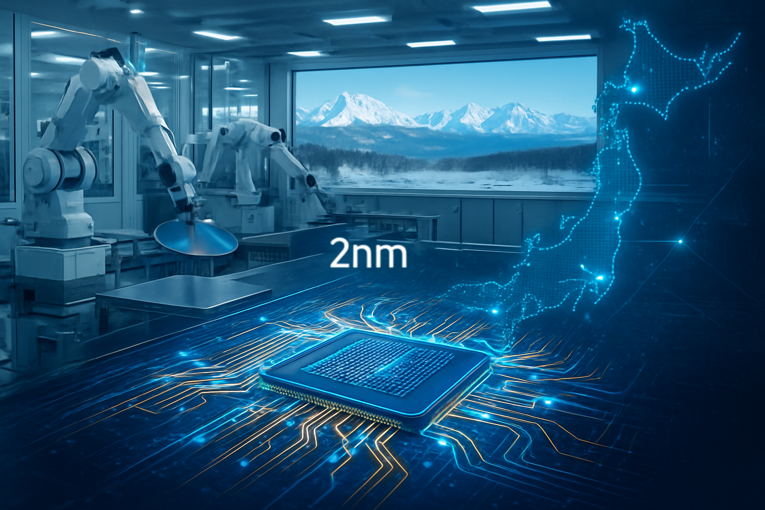
The venture—formed as a consortium of Japan’s leading industrial giants—is racing against a self-imposed 2027 deadline for mass production. With the successful completion of the cleanroom at its "IIM-1" facility in Chitose, Hokkaido, and the installation of the latest High-NA Extreme Ultraviolet (EUV) lithography machines from ASML Holding N.V. (NASDAQ:ASML), Rapidus is no longer a theoretical competitor. The company’s move into the pilot phase represents a significant geopolitical shift, reducing Japan’s reliance on foreign foundries and positioning the island of Hokkaido as a strategic "Silicon Road" to rival the established "Silicon Island" of Kyushu.
Engineering a Revolution: GAA Transistors and AI-Optimized Design
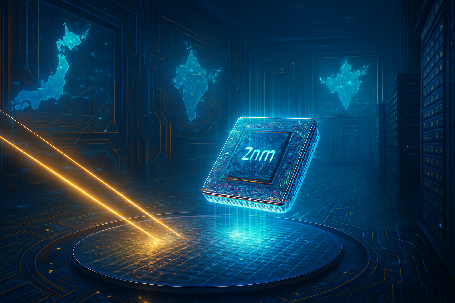
At the heart of the Rapidus mission is the transition to 2nm Gate-All-Around (GAA) transistor architecture. Unlike the FinFET structures used in previous generations, GAA technology surrounds the channel with the gate on all four sides, allowing for finer control over current, reduced power leakage, and significantly higher performance. In a recent technical update, Rapidus confirmed that its pilot line has successfully demonstrated working prototypes of these 2nm transistors, hitting the electrical characteristic targets required for high-performance computing (HPC) and advanced AI accelerators. This achievement was made possible through a deep technical transfer from International Business Machines Corp. (NYSE:IBM), which has served as a core research partner since the venture's inception.
What sets Rapidus apart from established giants like Taiwan Semiconductor Manufacturing Company (NYSE:TSM) is its "Rapid and Unified Manufacturing Service" (RUMS). Unlike the industry-standard "batch processing" model, which can take up to 120 days to cycle a wafer through a fab, Rapidus is utilizing a proprietary single-wafer processing system. This approach aims to slash cycle times to just 50 days, a feature specifically designed to appeal to AI startups and boutique chip designers who prioritize speed-to-market over sheer volume. To complement this hardware agility, the company recently launched "Raads" (Rapidus AI-Assisted Design Solution), a suite of tools that uses Large Language Models to help engineers optimize chip layouts for the 2nm node, effectively lowering the barrier to entry for custom silicon design.
Financial Foundations: SoftBank and Sony Lead the Charge
The technical progress has been matched by a surge in corporate confidence. In early February 2026, SoftBank Group Corp. (TYO:9984) and Sony Group Corp. (TYO:6758) each injected an additional 21 billion yen (approximately $135 million) into the venture, becoming its largest private shareholders. They were joined by Fujitsu Ltd. (TYO:6702), which contributed 20 billion yen, alongside continued support from existing backers like Toyota Motor Corp. (TYO:7203), Denso Corp. (TYO:6902), and Nippon Telegraph and Telephone Corp. (NTT) (TYO:9432). This collective investment, which is expected to exceed 160 billion yen for the current fiscal year, underscores a unified "Team Japan" strategy to secure the future of the nation’s technological sovereignty.
The Japanese government, through the Ministry of Economy, Trade and Industry (METI), has further solidified its role by providing nearly 2.9 trillion yen ($19 billion) in cumulative subsidies. Interestingly, the government has recently moved to take a "Golden Share" in Rapidus via the Information-technology Promotion Agency (IPA). This unique legal mechanism grants METI veto power over key decisions, such as the transfer of shares to foreign entities or changes in core technical partnerships. This level of state involvement highlights the fact that Rapidus is more than just a business venture; it is a critical component of Japanese national security policy in an era where silicon is as vital as oil.
Geopolitical Chess: The Hokkaido-Kumamoto Semiconductor Axis
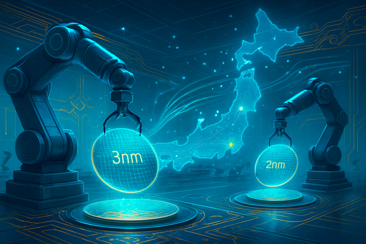
The rapid rise of Rapidus in Hokkaido creates a powerful dual-axis for Japanese manufacturing. While TSMC has focused its Japanese efforts in Kumamoto—where it recently upgraded its second factory to 3nm production—Rapidus is swinging for the fences with 2nm in the north. This geographical distribution is intentional, creating a "two-hub" system that mitigates risks from natural disasters and enhances the country's logistics network. While TSMC remains the undisputed king of high-volume manufacturing, Rapidus is positioning itself as the high-speed, high-tech alternative for the specialized AI market.
Industry analysts note that this competition is driving a massive influx of talent and infrastructure back to Japan. The presence of these two giants has revitalized the domestic equipment and materials sector, benefiting companies like Tokyo Electron and Screen Holdings. However, the strategic advantage for Rapidus lies in its relationship with the U.S. and Europe. By partnering with IBM and the Belgian research hub Imec, Rapidus has integrated itself into a "Western" semiconductor supply chain that is increasingly wary of over-concentration in the Taiwan Strait. This positioning makes Rapidus an attractive partner for U.S. hyperscalers who are looking to diversify their 2nm supply sources.
The 1.4nm Horizon: Overcoming Technical Barriers
Despite the momentum, the road to 2027 mass production remains fraught with technical challenges. The most pressing issue for Rapidus is achieving acceptable yield rates on a completely new transistor architecture. While the pilot line has been successful, scaling that to 30,000 wafers per month requires a level of manufacturing precision that few companies in history have mastered. Furthermore, critics point out that the initial 2027 roadmap for Rapidus lacks "Backside Power Delivery"—a revolutionary technique for routing power through the back of the wafer to improve efficiency—which both TSMC and Intel Corp. (NASDAQ:INTC) plan to deploy by the same timeframe.
Looking ahead, Rapidus has already begun preliminary research into the 1.4nm node to ensure it does not become a one-hit wonder. This includes exploring advanced packaging techniques, such as chiplets and hybrid bonding, at a dedicated R&D facility in collaboration with Seiko Epson Corp. (TYO:6724). The company must also address a looming talent shortage; while it has successfully recruited hundreds of veteran Japanese engineers, it needs to attract a new generation of digital natives to manage its AI-driven "Raads" design systems and automated fab environments.
A New Era for the Silicon Road
The emergence of Rapidus as a viable contender in the 2nm race is one of the most significant developments in the history of the semiconductor industry. It represents the successful convergence of state industrial policy, corporate collaboration, and international research partnerships. If Rapidus achieves its goal of mass production by late 2027, it will not only restore Japan’s reputation as a "chip powerhouse" but also provide the global AI industry with a much-needed alternative to the current foundry duopoly.
As we move through the first half of 2026, the focus will shift from construction and funding to execution and yield. The tech world will be watching closely as the first customer test chips emerge from the Hokkaido facility. For now, the "Silicon Road" is open, and Japan is driving forward at full speed. The coming months will determine if this 2nm moonshot can truly land, forever changing the landscape of high-performance computing and artificial intelligence.
This content is intended for informational purposes only and represents analysis of current AI developments.
TokenRing AI delivers enterprise-grade solutions for multi-agent AI workflow orchestration, AI-powered development tools, and seamless remote collaboration platforms.
For more information, visit https://www.tokenring.ai/.