Tag: Rubin Architecture

  • The Rubin Revolution: NVIDIA Unveils 2026 Roadmap to Cement AI Dominance Beyond Blackwell

    The Rubin Revolution: NVIDIA Unveils 2026 Roadmap to Cement AI Dominance Beyond Blackwell

    As the artificial intelligence industry continues its relentless expansion, NVIDIA (NASDAQ: NVDA) has officially pulled back the curtain on its next-generation architecture, codenamed "Rubin." Slated for a late 2026 release, the Rubin (R100) platform represents a pivotal shift in the company’s strategy, moving from a biennial release cycle to a blistering yearly cadence. This aggressive roadmap is designed to preemptively stifle competition and address the insatiable demand for the massive compute power required by next-generation frontier models.

    The announcement of Rubin comes at a time when the AI sector is transitioning from experimental pilot programs to industrial-scale "AI factories." By leapfrogging the current Blackwell architecture with a suite of radical technical innovations—including 3nm process technology and the first mass-market adoption of HBM4 memory—NVIDIA is signaling that it intends to remain the primary architect of the global AI infrastructure for the remainder of the decade.

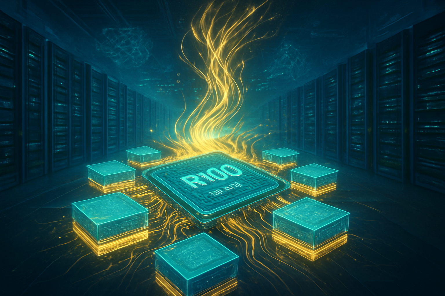
    Technical Deep Dive: 3nm Precision and the HBM4 Breakthrough

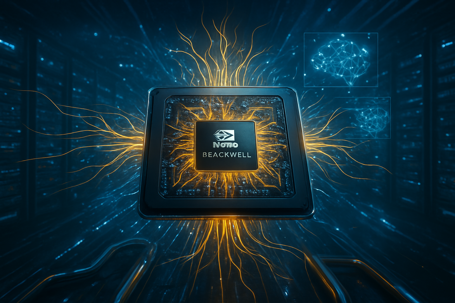
    The Rubin R100 GPU is a masterclass in semiconductor engineering, pushing the physical limits of what is possible in silicon fabrication. At its core, the architecture leverages TSMC (NYSE: TSM) N3P (3nm) process technology, a significant jump from the 4nm node used in the Blackwell generation. This transition allows for a massive increase in transistor density and, more importantly, a substantial improvement in energy efficiency—a critical factor as data center power constraints become the primary bottleneck for AI scaling.

    Perhaps the most significant technical advancement in the Rubin architecture is the implementation of a "4x reticle" design. While the previous Blackwell chips pushed the limits of lithography with a 3.3x reticle size, Rubin utilizes TSMC’s CoWoS-L packaging to integrate two massive, reticle-sized compute dies alongside two dedicated I/O tiles. This modular, chiplet-based approach allows NVIDIA to bypass the physical size limits of a single silicon wafer, effectively creating a "super-chip" that offers up to 50 petaflops of FP4 dense compute per socket—nearly triple the performance of the Blackwell B200.

    Complementing this raw compute power is the integration of HBM4 (High Bandwidth Memory 4). The R100 is expected to feature eight HBM4 stacks, providing a staggering 288GB of capacity and a memory bandwidth of 13 TB/s. This move is specifically designed to shatter the "memory wall" that has plagued large language model (LLM) training. By using a customized logic base die for the HBM4 stacks, NVIDIA has achieved lower latency and tighter integration than ever before, ensuring that the GPU's processing cores are never "starved" for data during the training of multi-trillion parameter models.

    The Competitive Moat: Yearly Cadence and Market Share

    NVIDIA’s shift to a yearly release cadence—moving from Blackwell in 2024 to Blackwell Ultra in 2025 and Rubin in 2026—is a strategic masterstroke aimed at maintaining its 80-90% market share. By accelerating its roadmap, NVIDIA forces competitors like AMD (NASDAQ: AMD) and Intel (NASDAQ: INTC) into a "generational lag." Just as rivals begin to ship hardware that competes with NVIDIA’s current flagship, the Santa Clara giant is already moving to the next iteration, effectively rendering the competition's "latest and greatest" obsolete upon arrival.

    This rapid refresh cycle also presents a significant challenge to the custom silicon efforts of hyperscalers. While Google (NASDAQ: GOOGL) with its TPU v7 and Amazon (NASDAQ: AMZN) with Trainium 3 have made significant strides in internalizing their AI workloads, NVIDIA’s sheer pace of innovation makes it difficult for internal teams to keep up. For many enterprises and "neoclouds," the certainty of NVIDIA’s performance lead outweighs the potential cost savings of custom silicon, especially when time-to-market for new AI capabilities is the primary competitive advantage.

    Furthermore, the Rubin architecture is not just a chip; it is a full-system refresh. The introduction of the "Vera" CPU—NVIDIA's successor to the Grace CPU—features custom "Olympus" cores that move away from off-the-shelf Arm designs. When paired with the R100 GPU in a "Vera Rubin Superchip," the system delivers unprecedented levels of performance-per-watt. This vertical integration of CPU, GPU, and networking (via the new 1.6 Tb/s X1600 switches) creates a proprietary ecosystem that is incredibly difficult for competitors to replicate, further entrenching NVIDIA’s dominance across the entire AI stack.

    Broader Significance: Power, Scaling, and the Future of AI Factories

    The Rubin roadmap arrives amidst a global debate over the sustainability of AI scaling. As models grow larger, the energy required to train and run them has become a matter of national security and environmental concern. The efficiency gains provided by the 3nm Rubin architecture are not just a technical "nice-to-have"; they are an existential necessity for the industry. By delivering more compute per watt, NVIDIA is enabling the continued scaling of AI without necessitating a proportional increase in global energy consumption.

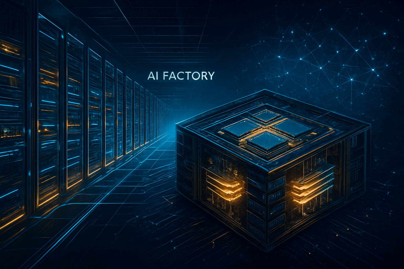
    This development also highlights the shift from "chips" to "racks" as the unit of compute. NVIDIA’s NVL144 and NVL576 systems, which will house the Rubin architecture, are essentially liquid-cooled supercomputers in a box. This transition signifies that the future of AI will be won not by those who make the best individual processors, but by those who can orchestrate thousands of interconnected dies into a single, cohesive "AI factory." This "system-on-a-rack" approach is what allows NVIDIA to maintain its premium pricing and high margins, even as the price of individual transistors continues to fall.

    However, the rapid pace of development also raises concerns about electronic waste and the capital expenditure (CapEx) burden on cloud providers. With hardware becoming "legacy" in just 12 to 18 months, the pressure on companies like Microsoft (NASDAQ: MSFT) and Meta to constantly refresh their infrastructure is immense. This "NVIDIA tax" is a double-edged sword: it drives the industry forward at breakneck speed, but it also creates a high barrier to entry that could centralize AI power in the hands of a few trillion-dollar entities.

    Future Horizons: Beyond Rubin to the Feynman Era

    Looking past 2026, NVIDIA has already teased its 2028 architecture, codenamed "Feynman." While details remain scarce, the industry expects Feynman to lean even more heavily into co-packaged optics (CPO) and photonics, replacing traditional copper interconnects with light-based data transfer to overcome the physical limits of electricity. The "Rubin Ultra" variant, expected in 2027, will serve as a bridge, introducing 12-Hi HBM4e memory and further refining the 3nm process.

    The challenges ahead are primarily physical and geopolitical. As NVIDIA approaches the 2nm and 1.4nm nodes with future architectures, the complexity of manufacturing will skyrocket, potentially leading to supply chain vulnerabilities. Additionally, as AI becomes a "sovereign" technology, export controls and trade tensions could impact NVIDIA’s ability to distribute its most advanced Rubin systems globally. Nevertheless, the roadmap suggests that NVIDIA is betting on a future where AI compute is as fundamental to the global economy as electricity or oil.

    Conclusion: A New Standard for the AI Era

    The Rubin architecture is more than just a hardware update; it is a declaration of intent. By committing to a yearly release cadence and pushing the boundaries of 3nm technology and HBM4 memory, NVIDIA is attempting to close the door on its competitors for the foreseeable future. The R100 GPU and Vera CPU represent the most sophisticated AI hardware ever conceived, designed specifically for the exascale requirements of the late 2020s.

    As we move toward 2026, the key metrics to watch will be the yield rates of TSMC’s 3nm process and the adoption of liquid-cooled rack systems by major data centers. If NVIDIA can successfully execute this transition, it will not only maintain its market dominance but also accelerate the arrival of "Artificial General Intelligence" (AGI) by providing the necessary compute substrate years ahead of schedule. For the tech industry, the message is clear: the Rubin era has begun, and the pace of innovation is only going to get faster.


    This content is intended for informational purposes only and represents analysis of current AI developments.

    TokenRing AI delivers enterprise-grade solutions for multi-agent AI workflow orchestration, AI-powered development tools, and seamless remote collaboration platforms.
    For more information, visit https://www.tokenring.ai/.

  • Nvidia’s Blackwell Dynasty: B200 and GB200 Sold Out Through Mid-2026 as Backlog Hits 3.6 Million Units

    Nvidia’s Blackwell Dynasty: B200 and GB200 Sold Out Through Mid-2026 as Backlog Hits 3.6 Million Units

    In a move that underscores the relentless momentum of the generative AI era, Nvidia (NASDAQ: NVDA) CEO Jensen Huang has confirmed that the company’s next-generation Blackwell architecture is officially sold out through mid-2026. During a series of high-level briefings and earnings calls in late 2025, Huang described the demand for the B200 and GB200 chips as "insane," noting that the global appetite for high-end AI compute has far outpaced even the most aggressive production ramps. This supply-demand imbalance has reached a fever pitch, with industry reports indicating a staggering backlog of 3.6 million units from the world’s largest cloud providers alone.

    The significance of this development cannot be overstated. As of December 29, 2025, Blackwell has become the definitive backbone of the global AI economy. The "sold out" status means that any enterprise or sovereign nation looking to build frontier-scale AI models today will likely have to wait over 18 months for the necessary hardware, or settle for previous-generation Hopper H100/H200 chips. This scarcity is not just a logistical hurdle; it is a geopolitical and economic bottleneck that is currently dictating the pace of innovation for the entire technology sector.

    The Technical Leap: 208 Billion Transistors and the FP4 Revolution

    The Blackwell B200 and GB200 represent the most significant architectural shift in Nvidia’s history, moving away from monolithic chip designs to a sophisticated dual-die "chiplet" approach. Each Blackwell GPU is composed of two primary dies connected by a massive 10 TB/s ultra-high-speed link, allowing them to function as a single, unified processor. This configuration enables a total of 208 billion transistors—a 2.6x increase over the 80 billion found in the previous H100. This leap in complexity is manufactured on a custom TSMC (NYSE: TSM) 4NP process, specifically optimized for the high-voltage requirements of AI workloads.

    Perhaps the most transformative technical advancement is the introduction of the FP4 (4-bit floating point) precision mode. By reducing the precision required for AI inference, Blackwell can deliver up to 20 PFLOPS of compute performance—roughly five times the throughput of the H100's FP8 mode. This allows for the deployment of trillion-parameter models with significantly lower latency. Furthermore, despite a peak power draw that can exceed 1,200W for a GB200 "Superchip," Nvidia claims the architecture is 25x more energy-efficient on a per-token basis than Hopper. This efficiency is critical as data centers hit the physical limits of power delivery and cooling.

    Initial reactions from the AI research community have been a mix of awe and frustration. While researchers at labs like OpenAI and Anthropic have praised the B200’s ability to handle "dynamic reasoning" tasks that were previously computationally prohibitive, the hardware's complexity has introduced new challenges. The transition to liquid cooling—a requirement for the high-density GB200 NVL72 racks—has forced a massive overhaul of data center infrastructure, leading to a "liquid cooling gold rush" for specialized components.

    The Hyperscale Arms Race: CapEx Surges and Product Delays

    The "sold out" status of Blackwell has intensified a multi-billion dollar arms race among the "Big Four" hyperscalers: Microsoft (NASDAQ: MSFT), Meta Platforms (NASDAQ: META), Alphabet (NASDAQ: GOOGL), and Amazon (NASDAQ: AMZN). Microsoft remains the lead customer, with quarterly capital expenditures (CapEx) surging to nearly $35 billion by late 2025 to secure its position as the primary host for OpenAI’s Blackwell-dependent models. Microsoft’s Azure ND GB200 V6 series has become the most coveted cloud instance in the world, often reserved months in advance by elite startups.

    Meta Platforms has taken an even more aggressive stance, with CEO Mark Zuckerberg projecting 2026 CapEx to exceed $100 billion. However, even Meta’s deep pockets couldn't bypass the physical reality of the backlog. The company was reportedly forced to delay the release of its most advanced "Llama 4 Behemoth" model until late 2025, as it waited for enough Blackwell clusters to come online. Similarly, Amazon’s AWS faced public scrutiny after its Blackwell Ultra (GB300) clusters were delayed, forcing the company to pivot toward its internal Trainium2 chips to satisfy customers who couldn't wait for Nvidia's hardware.

    The competitive landscape is now bifurcated between the "compute-rich" and the "compute-poor." Startups that secured early Blackwell allocations are seeing their valuations skyrocket, while those stuck on older H100 clusters are finding it increasingly difficult to compete on inference speed and cost. This has led to a strategic advantage for Oracle (NYSE: ORCL), which carved out a niche by specializing in rapid-deployment Blackwell clusters for mid-sized AI labs, briefly becoming the best-performing tech stock of 2025.

    Beyond the Silicon: Energy Grids and Geopolitics

    The wider significance of the Blackwell shortage extends far beyond corporate balance sheets. By late 2025, the primary constraint on AI expansion has shifted from "chips" to "kilowatts." A single large-scale Blackwell cluster consisting of 1 million GPUs is estimated to consume between 1.0 and 1.4 Gigawatts of power—enough to sustain a mid-sized city. This has placed immense strain on energy grids in Northern Virginia and Silicon Valley, leading Microsoft and Meta to invest directly in Small Modular Reactors (SMRs) and fusion energy research to ensure their future data centers have a dedicated power source.

    Geopolitically, the Blackwell B200 has become a tool of statecraft. Under the "SAFE CHIPS Act" of late 2025, the U.S. government has effectively banned the export of Blackwell-class hardware to China, citing national security concerns. This has accelerated China's reliance on domestic alternatives like Huawei’s Ascend series, creating a divergent AI ecosystem. Conversely, in a landmark deal in November 2025, the U.S. authorized the export of 70,000 Blackwell units to the UAE and Saudi Arabia, contingent on those nations shifting their AI partnerships exclusively toward Western firms and investing billions back into U.S. infrastructure.

    This era of "Sovereign AI" has seen nations like Japan and the UK scrambling to secure their own Blackwell allocations to avoid dependency on U.S. cloud providers. The Blackwell shortage has effectively turned high-end compute into a strategic reserve, comparable to oil in the 20th century. The 3.6 million unit backlog represents not just a queue of orders, but a queue of national and corporate ambitions waiting for the physical capacity to be realized.

    The Road to Rubin: What Comes After Blackwell

    Even as Nvidia struggles to fulfill Blackwell orders, the company has already provided a glimpse into the future with its "Rubin" (R100) architecture. Expected to enter mass production in late 2026, Rubin will move to TSMC’s 3nm process and utilize next-generation HBM4 memory from suppliers like SK Hynix and Micron (NASDAQ: MU). The Rubin R100 is projected to offer another 2.5x leap in FP4 compute performance, potentially reaching 50 PFLOPS per GPU.

    The transition to Rubin will be paired with the "Vera" CPU, forming the Vera Rubin Superchip. This new platform aims to address the memory bandwidth bottlenecks that still plague Blackwell clusters by offering a staggering 13 TB/s of bandwidth. Experts predict that the biggest challenge for the Rubin era will not be the chip design itself, but the packaging. TSMC’s CoWoS-L (Chip-on-Wafer-on-Substrate) capacity is already booked through 2027, suggesting that the "sold out" phenomenon may become a permanent fixture of the AI industry for the foreseeable future.

    In the near term, Nvidia is expected to release a "Blackwell Ultra" (B300) refresh in early 2026 to bridge the gap. This mid-cycle update will likely focus on increasing HBM3e capacity to 288GB per GPU, allowing for even larger models to be held in active memory. However, until the global supply chain for advanced packaging and high-bandwidth memory can scale by orders of magnitude, the industry will remain in a state of perpetual "compute hunger."

    Conclusion: A Defining Moment in AI History

    The 18-month sell-out of Nvidia’s Blackwell architecture marks a watershed moment in the history of technology. It is the first time in the modern era that the limiting factor for global economic growth has been reduced to a single specific hardware architecture. Jensen Huang’s "insane" demand is a reflection of a world that has fully committed to an AI-first future, where the ability to process data is the ultimate competitive advantage.

    As we look toward 2026, the key takeaways are clear: Nvidia’s dominance remains unchallenged, but the physical limits of power, cooling, and semiconductor packaging have become the new frontier. The 3.6 million unit backlog is a testament to the scale of the AI revolution, but it also serves as a warning about the fragility of a global economy dependent on a single supply chain.

    In the coming weeks and months, investors and tech leaders should watch for the progress of TSMC’s capacity expansions and any shifts in U.S. export policies. While Blackwell has secured Nvidia’s dynasty for the next two years, the race to build the infrastructure that can actually power these chips is only just beginning.


    This content is intended for informational purposes only and represents analysis of current AI developments.

    TokenRing AI delivers enterprise-grade solutions for multi-agent AI workflow orchestration, AI-powered development tools, and seamless remote collaboration platforms.
    For more information, visit https://www.tokenring.ai/.

  • TSMC Boosts CoWoS Capacity as NVIDIA Dominates Advanced Packaging Orders through 2027

    TSMC Boosts CoWoS Capacity as NVIDIA Dominates Advanced Packaging Orders through 2027

    As the artificial intelligence revolution enters its next phase of industrialization, the battle for compute supremacy has shifted from the transistor to the package. Taiwan Semiconductor Manufacturing Company (NYSE: TSM) is aggressively expanding its Chip on Wafer on Substrate (CoWoS) advanced packaging capacity, aiming for a 33% increase by 2026 to satisfy an insatiable global appetite for AI silicon. This expansion is designed to break the primary bottleneck currently stifling the production of next-generation AI accelerators.

    NVIDIA Corporation (NASDAQ: NVDA) has emerged as the undisputed anchor tenant of this new infrastructure, reportedly booking over 50% of TSMC’s projected CoWoS capacity for 2026. With an estimated 800,000 to 850,000 wafers reserved, NVIDIA is clearing the path for its upcoming Blackwell Ultra and the highly anticipated Rubin architectures. This strategic move ensures that while competitors scramble for remaining slots, the AI market leader maintains a stranglehold on the hardware required to power the world’s largest large language models (LLMs) and autonomous systems.

    The Technical Frontier: CoWoS-L, SoIC, and the Rubin Shift

    The technical complexity of AI chips has reached a point where traditional monolithic designs are no longer viable. TSMC’s CoWoS technology, specifically the CoWoS-L (Local Silicon Interconnect) variant, has become the gold standard for integrating multiple logic and memory dies. As of late 2025, the industry is transitioning from the Blackwell architecture to Blackwell Ultra (GB300), which pushes the limits of interposer size. However, the real technical leap lies in the Rubin (R100) architecture, which utilizes a massive 4x reticle design. This means each chip occupies significantly more physical space on a wafer, necessitating the 33% capacity boost just to maintain current unit volume delivery.

    Rubin represents a paradigm shift by combining CoWoS-L with System on Integrated Chips (SoIC) technology. This "3D" stacking approach allows for shorter vertical interconnects, drastically reducing power consumption while increasing bandwidth. Furthermore, the Rubin platform will be the first to integrate High Bandwidth Memory 4 (HBM4) on TSMC’s N3P (3nm) process. Industry experts note that the integration of HBM4 requires unprecedented precision in bonding, a capability TSMC is currently perfecting at its specialized facilities.

    The initial reaction from the AI research community has been one of cautious optimism. While the technical specs of Rubin suggest a 3x to 5x performance-per-watt improvement over Blackwell, there are concerns regarding the "memory wall." As compute power scales, the ability of the packaging to move data between the processor and memory remains the ultimate governor of performance. TSMC’s ability to scale SoIC and CoWoS in tandem is seen as the only viable solution to this hardware constraint through 2027.

    Market Dominance and the Competitive Squeeze

    NVIDIA’s decision to lock down more than half of TSMC’s advanced packaging capacity through 2027 creates a challenging environment for other fabless chip designers. Companies like Advanced Micro Devices (NASDAQ: AMD) and specialized AI chip startups are finding themselves in a fierce bidding war for the remaining 40-50% of CoWoS supply. While AMD has successfully utilized TSMC’s packaging for its MI300 and MI350 series, the sheer scale of NVIDIA’s orders threatens to push competitors toward alternative Outsourced Semiconductor Assembly and Test (OSAT) providers like ASE Technology Holding (NYSE: ASX) or Amkor Technology (NASDAQ: AMKR).

    Hyperscalers such as Microsoft (NASDAQ: MSFT), Amazon (NASDAQ: AMZN), and Alphabet (NASDAQ: GOOGL) are also impacted by this capacity crunch. While these tech giants are increasingly designing their own custom AI silicon (like Azure’s Maia or Google’s TPU), they still rely heavily on TSMC for both wafer fabrication and advanced packaging. NVIDIA’s dominance in the packaging queue could potentially delay the rollout of internal silicon projects at these firms, forcing continued reliance on NVIDIA’s off-the-shelf H100, B200, and future Rubin systems.

    Strategic advantages are also shifting toward the memory manufacturers. SK Hynix, Micron Technology (NASDAQ: MU), and Samsung are now integral parts of the CoWoS ecosystem. Because HBM4 must be physically bonded to the logic die during the CoWoS process, these companies must coordinate their production cycles perfectly with TSMC’s expansion. The result is a more vertically integrated supply chain where NVIDIA and TSMC act as the central orchestrators, dictating the pace of innovation for the entire semiconductor industry.

    Geopolitics and the Global Infrastructure Landscape

    The expansion of TSMC’s capacity is not limited to Taiwan. The company’s Chiayi AP7 plant is central to this strategy, featuring multiple phases designed to scale through 2028. However, the geopolitical pressure to diversify the supply chain has led to significant developments in the United States. As of December 2025, TSMC has accelerated plans for an advanced packaging facility in Arizona. While Arizona’s Fab 21 is already producing 4nm and 5nm wafers with high yields, the lack of local packaging has historically required those wafers to be shipped back to Taiwan for final assembly—a process known as the "packaging gap."

    To address this, TSMC is repurposing land in Arizona for a dedicated Advanced Packaging (AP) plant, with tool move-in expected by late 2027. This move is seen as a critical step in de-risking the AI supply chain from potential cross-strait tensions. By providing "end-to-end" manufacturing on U.S. soil, TSMC is aligning itself with the strategic interests of the U.S. government while ensuring that its largest customer, NVIDIA, has a resilient path to market for its most sensitive government and enterprise contracts.

    This shift mirrors previous milestones in the semiconductor industry, such as the transition to EUV (Extreme Ultraviolet) lithography. Just as EUV became the gatekeeper for sub-7nm chips, advanced packaging is now the gatekeeper for the AI era. The massive capital expenditure required—estimated in the tens of billions of dollars—ensures that only a handful of players can compete at the leading edge, further consolidating power within the TSMC-NVIDIA-HBM triad.

    Future Horizons: Beyond 2027 and the Rise of Panel-Level Packaging

    Looking beyond 2027, the industry is already eyeing the next evolution: Chip-on-Panel-on-Substrate (CoPoS). As AI chips continue to grow in size, the circular 300mm silicon wafer becomes an inefficient medium for packaging. Panel-level packaging, which uses large rectangular glass or organic substrates, offers the potential to process significantly more chips at once, potentially lowering costs and increasing throughput. TSMC is reportedly experimenting with this technology at its later-phase AP7 facilities in Chiayi, with mass production targets set for the 2028-2029 timeframe.

    In the near term, we can expect a flurry of activity around HBM4 and HBM4e integration. The transition to 12-high and 16-high memory stacks will require even more sophisticated bonding techniques, such as hybrid bonding, which eliminates the need for traditional "bumps" between dies. This will allow for even thinner, more powerful AI modules that can fit into the increasingly cramped environments of edge servers and high-density data centers.

    The primary challenge remaining is the thermal envelope. As Rubin and its successors pack more transistors and memory into smaller volumes, the heat generated is becoming a physical limit. Future developments will likely include integrated liquid cooling or even "optical" interconnects that use light instead of electricity to move data between chips, further evolving the definition of what a "package" actually is.

    A New Era of Integrated Silicon

    TSMC’s aggressive expansion of CoWoS capacity and NVIDIA’s massive pre-orders mark a definitive turning point in the AI hardware race. We are no longer in an era where software alone defines AI progress; the physical constraints of how chips are assembled and cooled have become the primary variables in the equation of intelligence. By securing the lion's share of TSMC's capacity, NVIDIA has not just bought chips—it has bought time and market stability through 2027.

    The significance of this development cannot be overstated. It represents the maturation of the AI supply chain from a series of experimental bursts into a multi-year industrial roadmap. For the tech industry, the focus for the next 24 months will be on execution: can TSMC bring the AP7 and Arizona facilities online fast enough to meet the demand, and can the memory manufacturers keep up with the transition to HBM4?

    As we move into 2026, the industry should watch for the first risk production of the Rubin architecture and any signs of "over-ordering" that could lead to a future inventory correction. For now, however, the signal is clear: the AI boom is far from over, and the infrastructure to support it is being built at a scale and speed never before seen in the history of computing.


    This content is intended for informational purposes only and represents analysis of current AI developments.

    TokenRing AI delivers enterprise-grade solutions for multi-agent AI workflow orchestration, AI-powered development tools, and seamless remote collaboration platforms.
    For more information, visit https://www.tokenring.ai/.

  • The Silicon Supercycle: NVIDIA and Marvell Set to Redefine AI Infrastructure in 2026

    The Silicon Supercycle: NVIDIA and Marvell Set to Redefine AI Infrastructure in 2026

    As we stand at the threshold of 2026, the artificial intelligence semiconductor market has transcended its status as a high-growth niche to become the foundational engine of the global economy. With the total addressable market for AI silicon projected to hit $121.7 billion this year, the industry is witnessing a historic "supercycle" driven by an insatiable demand for compute power. While 2025 was defined by the initial ramp of Blackwell GPUs, 2026 is shaping up to be the year of architectural transition, where the focus shifts from raw training capacity to massive-scale inference and sovereign AI infrastructure.

    The landscape is currently dominated by two distinct but complementary forces: the relentless innovation of NVIDIA (NASDAQ:NVDA) in general-purpose AI hardware and the strategic rise of Marvell Technology (NASDAQ:MRVL) in the custom silicon and connectivity space. As hyperscalers like Microsoft (NASDAQ:MSFT) and Alphabet (NASDAQ:GOOGL) prepare to deploy capital expenditures exceeding $500 billion collectively in 2026, the battle for silicon supremacy has moved to the 2-nanometer (2nm) frontier, where energy efficiency and interconnect bandwidth are the new currencies of power.

    The Leap to 2nm and the Rise of the Rubin Architecture

    The technical narrative of 2026 is dominated by the transition to the 2nm manufacturing node, led by Taiwan Semiconductor Manufacturing Company (NYSE:TSM). This shift introduces Gate-All-Around (GAA) transistor architecture, which offers a 45% reduction in power consumption compared to the aging 5nm standards. For NVIDIA, this technological leap is the backbone of its next-generation "Vera Rubin" platform. While the Blackwell Ultra (B300) remains the workhorse for enterprise data centers in early 2026, the second half of the year will see the mass deployment of the Rubin R100 series.

    The Rubin architecture represents a paradigm shift in AI hardware design. Unlike previous generations that focused primarily on floating-point operations per second (FLOPS), Rubin is engineered for the "inference era." It integrates the new Vera CPU, which doubles chip-to-chip bandwidth to 1,800 GB/s, and utilizes HBM4 memory—the first generation of High Bandwidth Memory to offer 13 TB/s of bandwidth. This allows for the processing of trillion-parameter models with a fraction of the latency seen in 2024-era hardware. Industry experts note that the Rubin CPX, a specialized variant of the GPU, is specifically designed for massive-context inference, addressing the growing need for AI models that can "remember" and process vast amounts of real-time data.

    The reaction from the research community has been one of cautious optimism regarding the energy-to-performance ratio. Early benchmarks suggest that Rubin systems will provide a 3.3x performance boost over Blackwell Ultra configurations. However, the complexity of 2nm fabrication has led to a projected 50% price hike for wafers, sparking a debate about the sustainability of hardware costs. Despite this, the demand remains "sold out" through most of 2026, as the industry's largest players race to secure the first batches of 2nm silicon to maintain their competitive edge in the AGI (Artificial General Intelligence) race.

    Custom Silicon and the Optical Interconnect Revolution

    While NVIDIA captures the headlines with its flagship GPUs, Marvell Technology (NASDAQ:MRVL) has quietly become the indispensable "plumbing" of the AI data center. In 2026, Marvell's data center revenue is expected to account for over 70% of its total business, driven by two critical sectors: custom Application-Specific Integrated Circuits (ASICs) and high-speed optical connectivity. As hyperscalers like Amazon (NASDAQ:AMZN) and Meta (NASDAQ:META) seek to reduce their total cost of ownership and reliance on third-party silicon, they are increasingly turning to Marvell to co-develop custom AI accelerators.

    Marvell’s custom ASIC business is projected to grow by 25% in 2026, positioning it as a formidable challenger to Broadcom (NASDAQ:AVGO). These custom chips are optimized for specific internal workloads, such as recommendation engines or video processing, providing better efficiency than general-purpose GPUs. Furthermore, Marvell has pioneered the transition to 1.6T PAM4 DSPs (Digital Signal Processors), which are essential for the optical interconnects that link tens of thousands of GPUs into a single "supercomputer." As clusters scale to 100,000+ units, the bottleneck is no longer the chip itself, but the speed at which data can move between them.

    The strategic advantage for Marvell lies in its early adoption of Co-Packaged Optics (CPO) and its acquisition of photonic fabric specialists. By integrating optical connectivity directly onto the chip package, Marvell is addressing the "power wall"—the point at which moving data consumes more energy than processing it. This has created a symbiotic relationship where NVIDIA provides the "brains" of the data center, while Marvell provides the "nervous system." Competitive implications are significant; companies that fail to master these high-speed interconnects in 2026 will find their hardware clusters underutilized, regardless of how fast their individual GPUs are.

    Sovereign AI and the Shift to Global Infrastructure

    The broader significance of the 2026 semiconductor outlook lies in the emergence of "Sovereign AI." Nations are no longer content to rely on a few Silicon Valley giants for their AI needs; instead, they are treating AI compute as a matter of national security and economic sovereignty. Significant projects, such as the UK’s £18 billion "Stargate UK" cluster and Saudi Arabia’s $100 billion "Project Transcendence," are driving a new wave of demand that is decoupled from the traditional tech cycle. These projects require specialized, secure, and often localized semiconductor supply chains.

    This trend is also forcing a shift from AI training to AI inference. In 2024 and 2025, the market was obsessed with training larger and larger models. In 2026, the focus has moved to "serving" those models to billions of users. Inference workloads are growing at a faster compound annual growth rate (CAGR) than training, which favors hardware that can operate efficiently at the edge and in smaller regional data centers. This shift is beneficial for companies like Intel (NASDAQ:INTC) and Samsung (KRX:005930), who are aggressively courting custom silicon customers with their own 2nm and 18A process nodes as alternatives to TSMC.

    However, this massive expansion comes with significant environmental and logistical concerns. The "Gigawatt-scale" data centers of 2026 are pushing local power grids to their limits. This has made liquid cooling a standard requirement for high-density racks, creating a secondary market for thermal management technologies. The comparison to previous milestones, such as the mobile internet revolution or the shift to cloud computing, falls short; the AI silicon boom is moving at a velocity that requires a total redesign of power, cooling, and networking infrastructure every 12 to 18 months.

    Future Horizons: Beyond 2nm and the Road to 2027

    Looking toward the end of 2026 and into 2027, the industry is already preparing for the sub-2nm era. TSMC and its competitors are already outlining roadmaps for 1.4nm nodes, which will likely utilize even more exotic materials and transistor designs. The near-term development to watch is the integration of AI-driven design tools—AI chips designed by AI—which is expected to accelerate the development cycle of new architectures even further.

    The primary challenge remains the "energy gap." While 2nm GAA transistors are more efficient, the sheer volume of chips being deployed means that total energy consumption continues to rise. Experts predict that the next phase of innovation will focus on "neuromorphic" computing and alternative architectures that mimic the human brain's efficiency. In the meantime, the industry must navigate the geopolitical complexities of semiconductor manufacturing, as the concentration of advanced node production in East Asia remains a point of strategic vulnerability for the global economy.

    A New Era of Computing

    The AI semiconductor market of 2026 represents the most significant technological pivot of the 21st century. NVIDIA’s transition to the Rubin architecture and Marvell’s dominance in custom silicon and optical fabrics are not just corporate success stories; they are the blueprints for the next era of human productivity. The move to 2nm manufacturing and the rise of sovereign AI clusters signify that we have moved past the "experimental" phase of AI and into the "infrastructure" phase.

    As we move through 2026, the key metrics for success will no longer be just TFLOPS or wafer yields, but rather "performance-per-watt" and "interconnect-latency." The coming months will be defined by the first real-world deployments of 2nm Rubin systems and the continued expansion of custom ASIC programs among the hyperscalers. For investors and industry observers, the message is clear: the silicon supercycle is just getting started, and the foundations laid in 2026 will determine the trajectory of artificial intelligence for the next decade.


    This content is intended for informational purposes only and represents analysis of current AI developments.

    TokenRing AI delivers enterprise-grade solutions for multi-agent AI workflow orchestration, AI-powered development tools, and seamless remote collaboration platforms.
    For more information, visit https://www.tokenring.ai/.

  • The Nvidia Paradox: Why a $4.3 Trillion Valuation is Just the Beginning

    The Nvidia Paradox: Why a $4.3 Trillion Valuation is Just the Beginning

    As of December 19, 2025, Nvidia (NASDAQ:NVDA) has achieved a feat once thought impossible: maintaining a market valuation of $4.3 trillion while simultaneously being labeled as "cheap" by a growing chorus of Wall Street analysts. While the sheer magnitude of the company's market cap makes it the most valuable entity on Earth—surpassing the likes of Apple (NASDAQ:AAPL) and Microsoft (NASDAQ:MSFT)—the financial metrics underlying this growth suggest that the market may still be underestimating the velocity of the artificial intelligence revolution.

    The "Nvidia Paradox" refers to the counter-intuitive reality where a stock's price rises by triple digits, yet its valuation multiples actually shrink. This phenomenon is driven by earnings growth that is outstripping even the most bullish stock price targets. As the world shifts from general-purpose computing to accelerated computing and generative AI, Nvidia has positioned itself not just as a chip designer, but as the primary architect of the global "AI Factory" infrastructure.

    The Math Behind the 'Bargain'

    The primary driver for the "cheap" designation is Nvidia’s forward price-to-earnings (P/E) ratio. Despite the $4.3 trillion valuation, the stock is currently trading at approximately 24x to 25x its projected earnings for the next fiscal year. To put this in perspective, this multiple places Nvidia in the 11th percentile of its historical valuation over the last decade. For nearly 90% of the past ten years, investors were paying a higher premium for Nvidia's earnings than they are today, even though the company's competitive moat has never been wider.

    Furthermore, the Price/Earnings-to-Growth (PEG) ratio—a favorite metric for growth investors—has dipped below 0.7x. In traditional valuation theory, any PEG ratio under 1.0 is considered undervalued. This suggests that the market has not fully priced in the 50% to 60% revenue growth projected for 2026. This disconnect is largely due to the massive earnings compression caused by the Blackwell architecture's rollout, which has seen unprecedented demand, with systems reportedly sold out for the next four quarters.

    Technically, the transition from the Blackwell B200 series to the upcoming Rubin R100 platform is the catalyst for this sustained growth. While Blackwell focused on massive efficiency gains in training, the Rubin architecture—utilizing Taiwan Semiconductor Manufacturing Co.'s (NYSE:TSM) 3nm process and next-generation HBM4 memory—is designed to treat an entire data center as a single, unified computer. This "rack-scale" approach makes it increasingly difficult for analysts to compare Nvidia to traditional semiconductor firms like Intel (NASDAQ:INTC) or AMD (NASDAQ:AMD), as Nvidia is effectively selling entire "AI Factories" rather than individual components.

    Initial reactions from the industry highlight that Nvidia’s move to a one-year release cycle (Blackwell in 2024, Rubin in 2026) has created a "velocity gap" that competitors are struggling to bridge. Industry experts note that by the time rivals release a chip to compete with Blackwell, Nvidia is already shipping Rubin, effectively resetting the competitive clock every twelve months.

    The Infrastructure Moat and the Hyperscaler Arms Race

    The primary beneficiaries of Nvidia’s continued dominance are the "Hyperscalers"—Microsoft, Alphabet (NASDAQ:GOOGL), Amazon (NASDAQ:AMZN), and Meta (NASDAQ:META). These companies have collectively committed over $400 billion in capital expenditures for 2025, a significant portion of which is flowing directly into Nvidia’s coffers. For these tech giants, the risk of under-investing in AI infrastructure is far greater than the risk of over-spending, as AI becomes the core engine for cloud services, search, and social media recommendation algorithms.

    Nvidia’s strategic advantage is further solidified by its CUDA software ecosystem, which remains the industry standard for AI development. While companies like AMD (NASDAQ:AMD) have made strides with their MI300 and MI350 series chips, the "switching costs" for moving away from Nvidia’s software stack are prohibitively high for most enterprise customers. This has allowed Nvidia to capture over 90% of the data center GPU market, leaving competitors to fight for the remaining niche segments.

    The potential disruption to existing services is profound. As Nvidia scales its "AI Factories," traditional CPU-based data centers are becoming obsolete for modern workloads. This has forced a massive re-architecting of the global cloud, where the value is shifting from general-purpose processing to specialized AI inference. This shift favors Nvidia’s integrated systems, such as the NVL72 rack, which integrates 72 GPUs and 36 CPUs into a single liquid-cooled unit, providing a level of performance that standalone chips cannot match.

    Strategically, Nvidia has also insulated itself from potential spending plateaus by Big Tech. By diversifying into enterprise AI and "Sovereign AI," the company has tapped into national budgets and public sector capital, creating a secondary layer of demand that is less sensitive to the cyclical nature of the consumer tech market.

    Sovereign AI: The New Industrial Revolution

    Perhaps the most significant development in late 2025 is the rise of "Sovereign AI." Nations such as Japan, France, Saudi Arabia, and the United Kingdom have begun treating AI capabilities as a matter of national security and digital autonomy. This shift represents a "New Industrial Revolution," where data is the raw material and Nvidia’s AI Factories are the refineries. By building domestic AI infrastructure, these nations ensure that their cultural values, languages, and sensitive data remain within their own borders.

    This movement has transformed Nvidia from a silicon vendor into a geopolitical partner. Sovereign AI initiatives are projected to contribute over $20 billion to Nvidia’s revenue in the coming fiscal year, providing a hedge against any potential cooling in the U.S. cloud market. This trend mirrors the historical development of national power grids or telecommunications networks; countries that do not own their AI infrastructure risk becoming "digital colonies" of foreign tech powers.

    Comparisons to previous milestones, such as the mobile internet or the dawn of the web, often fall short because of the speed of AI adoption. While the internet took decades to fully transform the global economy, the transition to AI-driven productivity is happening in a matter of years. The "Inference Era"—the phase where AI models are not just being trained but are actively running millions of tasks per second—is driving a recurring demand for "intelligence tokens" that functions more like a utility than a traditional hardware cycle.

    However, this dominance does not come without concerns. Antitrust scrutiny in the U.S. and Europe remains a persistent headwind, as regulators worry about Nvidia’s "full-stack" lock-in. Furthermore, the immense power requirements of AI Factories have sparked a global race for energy solutions, leading Nvidia to partner with energy providers to optimize the power-to-performance ratio of its massive GPU clusters.

    The Road to Rubin and Beyond

    Looking ahead to 2026, the tech world is focused on the mass production of the Rubin architecture. Named after astronomer Vera Rubin, this platform will feature the new "Vera" CPU and HBM4 memory, promising a 3x performance leap over Blackwell. This rapid cadence is designed to keep Nvidia ahead of the "AI scaling laws," which dictate that as models grow larger, they require exponentially more compute power to remain efficient.

    In the near term, expect to see Nvidia move deeper into the field of physical AI and humanoid robotics. The company’s GR00T project, a foundation model for humanoid robots, is expected to see its first large-scale industrial deployments in 2026. This expands Nvidia’s Total Addressable Market (TAM) from the data center to the factory floor, as AI begins to interact with and manipulate the physical world.

    The challenge for Nvidia will be managing its massive supply chain. Producing 1,000 AI racks per week is a logistical feat that requires flawless execution from partners like TSMC and SK Hynix. Any disruption in the semiconductor supply chain or a geopolitical escalation in the Taiwan Strait remains the primary "black swan" risk for the company’s $4.3 trillion valuation.

    A New Benchmark for the Intelligence Age

    The Nvidia Paradox serves as a reminder that in a period of exponential technological change, traditional valuation metrics can be misleading. A $4.3 trillion market cap is a staggering number, but when viewed through the lens of a 25x forward P/E and a 0.7x PEG ratio, the stock looks more like a value play than a speculative bubble. Nvidia has successfully transitioned from a gaming chip company to the indispensable backbone of the global intelligence economy.

    Key takeaways for investors and industry observers include the company's shift toward a one-year innovation cycle, the emergence of Sovereign AI as a major revenue pillar, and the transition from model training to large-scale inference. As we head into 2026, the primary metric to watch will be the "utilization of intelligence"—how effectively companies and nations can turn their massive investments in Nvidia hardware into tangible economic productivity.

    The coming months will likely see further volatility as the market digests these massive figures, but the underlying trend is clear: the demand for compute is the new oil of the 21st century. As long as Nvidia remains the only company capable of refining that oil at scale, its "expensive" valuation may continue to be the biggest bargain in tech.


    This content is intended for informational purposes only and represents analysis of current AI developments.

    TokenRing AI delivers enterprise-grade solutions for multi-agent AI workflow orchestration, AI-powered development tools, and seamless remote collaboration platforms.
    For more information, visit https://www.tokenring.ai/.

  • Beyond the Chip: Nvidia’s Rubin Architecture Ushers in the Era of the Gigascale AI Factory

    Beyond the Chip: Nvidia’s Rubin Architecture Ushers in the Era of the Gigascale AI Factory

    As 2025 draws to a close, the semiconductor landscape is bracing for its most significant transformation yet. NVIDIA (NASDAQ: NVDA) has officially moved into the sampling phase for its highly anticipated Rubin architecture, the successor to the record-breaking Blackwell generation. While Blackwell focused on scaling the GPU to its physical limits, Rubin represents a fundamental pivot in silicon engineering: the transition from individual accelerators to "AI Factories"—massive, multi-die systems designed to treat an entire data center as a single, unified computer.

    This shift comes at a critical juncture as the industry moves toward "Agentic AI" and million-token context windows. The Rubin platform is not merely a faster processor; it is a holistic re-architecting of compute, memory, and networking. By integrating next-generation HBM4 memory and the new Vera CPU, Nvidia is positioning itself to maintain its near-monopoly on high-end AI infrastructure, even as competitors and cloud providers attempt to internalize their chip designs.

    The Technical Blueprint: R100, Vera, and the HBM4 Revolution

    At the heart of the Rubin platform is the R100 GPU, a marvel of 3nm engineering manufactured by Taiwan Semiconductor Manufacturing Company (NYSE: TSM). Unlike previous generations that pushed the limits of a single reticle, the R100 utilizes a sophisticated multi-die design enabled by TSMC’s CoWoS-L packaging. Each R100 package consists of two primary compute dies and dedicated I/O tiles, effectively doubling the silicon area available for logic. This allows a single Rubin package to deliver an astounding 50 PFLOPS of FP4 precision compute, roughly 2.5 times the performance of a Blackwell GPU.

    Complementing the GPU is the Vera CPU, Nvidia’s successor to the Grace processor. Vera features 88 custom Arm-based cores designed specifically for AI orchestration and data pre-processing. The interconnect between the CPU and GPU has been upgraded to NVLink-C2C, providing a staggering 1.8 TB/s of bandwidth. Perhaps most significant is the debut of HBM4 (High Bandwidth Memory 4). Supplied by partners like SK Hynix (KRX: 000660) and Micron (NASDAQ: MU), the Rubin GPU features 288GB of HBM4 capacity with a bandwidth of 13.5 TB/s, a necessity for the trillion-parameter models expected to dominate 2026.

    Beyond raw power, Nvidia has introduced a specialized component called the Rubin CPX. This "Context Accelerator" is designed specifically for the prefill stage of large language model (LLM) inference. By using high-speed GDDR7 memory and specialized hardware for attention mechanisms, the CPX addresses the "memory wall" that often bottlenecks long-context window tasks, such as analyzing entire codebases or hour-long video files.

    Market Dominance and the Competitive Moat

    The move to the Rubin architecture solidifies Nvidia’s strategic advantage over rivals like AMD (NASDAQ: AMD) and Intel (NASDAQ: INTC). By moving to an annual release cadence and a "system-level" product, Nvidia is forcing competitors to compete not just with a chip, but with an entire rack-scale ecosystem. The Vera Rubin NVL144 system, which integrates 144 GPU dies and 36 Vera CPUs into a single liquid-cooled rack, is designed to be the "unit of compute" for the next generation of cloud infrastructure.

    Major cloud service providers (CSPs) including Amazon (NASDAQ: AMZN), Microsoft (NASDAQ: MSFT), and Alphabet (NASDAQ: GOOGL) are already lining up for early Rubin shipments. While these companies have developed their own internal AI chips (such as Trainium and TPU), the sheer software ecosystem of Nvidia’s CUDA, combined with the interconnect performance of NVLink 6, makes Rubin the indispensable choice for frontier model training. This puts pressure on secondary hardware players, as the barrier to entry is no longer just silicon performance, but the ability to provide a multi-terabit networking fabric that can scale to millions of interconnected units.

    Scaling the AI Factory: Implications for the Global Landscape

    The Rubin architecture marks the official arrival of the "AI Factory" era. Nvidia’s vision is to transform the data center from a collection of servers into a production line for intelligence. This has profound implications for global energy consumption and infrastructure. A single NVL576 Rubin Ultra rack is expected to draw upwards of 600kW of power, requiring advanced 800V DC power delivery and sophisticated liquid-to-liquid cooling systems. This shift is driving a secondary boom in the industrial cooling and power management sectors.

    Furthermore, the Rubin generation highlights the growing importance of silicon photonics. To bridge the gap between racks without the latency of traditional copper wiring, Nvidia is integrating optical interconnects directly into its X1600 switches. This "Giga-scale" networking allows a cluster of 100,000 GPUs to behave as if they were on a single circuit board. While this enables unprecedented AI breakthroughs, it also raises concerns about the centralization of AI power, as only a handful of nations and corporations can afford the multi-billion-dollar price tag of a Rubin-powered factory.

    The Horizon: Rubin Ultra and the Path to AGI

    Looking ahead to 2026 and 2027, Nvidia has already teased the Rubin Ultra variant. This iteration is expected to push memory capacities toward 1TB per GPU package using 16-high HBM4e stacks. The industry predicts that this level of memory density will be the catalyst for "World Models"—AI systems capable of simulating complex physical environments in real-time for robotics and autonomous vehicles.

    The primary challenge facing the Rubin rollout remains the supply chain. The reliance on TSMC’s advanced 3nm nodes and the high-precision assembly required for CoWoS-L packaging means that supply will likely remain constrained throughout 2026. Experts also point to the "software tax," where the complexity of managing a multi-die, rack-scale system requires a new generation of orchestration software that can handle hardware failures and data sharding at an unprecedented scale.

    A New Benchmark for Artificial Intelligence

    The Rubin architecture is more than a generational leap; it is a statement of intent. By moving to a multi-die, system-centric model, Nvidia has effectively redefined what it means to build AI hardware. The integration of the Vera CPU, HBM4, and NVLink 6 creates a vertically integrated powerhouse that will likely define the state-of-the-art for the next several years.

    As we move into 2026, the industry will be watching the first deployments of the Vera Rubin NVL144 systems. If these "AI Factories" deliver on their promise of 2.5x performance gains and seamless long-context processing, the path toward Artificial General Intelligence (AGI) may be paved with Nvidia silicon. For now, the tech world remains in a state of high anticipation, as the first Rubin samples begin to land in the labs of the world’s leading AI researchers.


    This content is intended for informational purposes only and represents analysis of current AI developments.

    TokenRing AI delivers enterprise-grade solutions for multi-agent AI workflow orchestration, AI-powered development tools, and seamless remote collaboration platforms.
    For more information, visit https://www.tokenring.ai/.