Tag: Samsung

  • The Packaging Wars: Why Advanced Packaging Has Replaced Transistor Counts as the Throne of AI Supremacy

    The Packaging Wars: Why Advanced Packaging Has Replaced Transistor Counts as the Throne of AI Supremacy

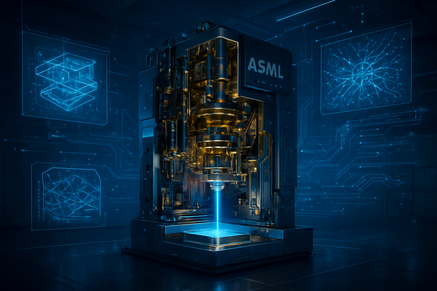
    As of December 18, 2025, the semiconductor industry has reached a historic inflection point where the traditional metric of progress—raw transistor density—has been unseated by a more complex and critical discipline: advanced packaging. For decades, Moore’s Law dictated that doubling the number of transistors on a single slice of silicon every two years was the primary path to performance. However, as the industry pushes toward the 2nm and 1.4nm nodes, the physical and economic costs of shrinking transistors have become prohibitive. In their place, technologies like Chip-on-Wafer-on-Substrate (CoWoS) and high-density chiplet interconnects have become the true gatekeepers of the generative AI revolution, determining which companies can build the massive "super-chips" required for the next generation of Large Language Models (LLMs).

    The immediate significance of this shift is visible in the supply chain bottlenecks that defined much of 2024 and 2025. While foundries could print the chips, they couldn't "wrap" them fast enough. Today, the ability to stitch together multiple specialized dies—logic, memory, and I/O—into a single, cohesive package is what separates flagship AI accelerators like NVIDIA’s (NASDAQ: NVDA) Rubin architecture from its predecessors. This transition from "System-on-Chip" (SoC) to "System-on-Package" (SoP) represents the most significant architectural change in computing since the invention of the integrated circuit, allowing chipmakers to bypass the physical "reticle limit" that once capped the size and power of a single processor.

    The Technical Frontier: Breaking the Reticle Limit and the Memory Wall

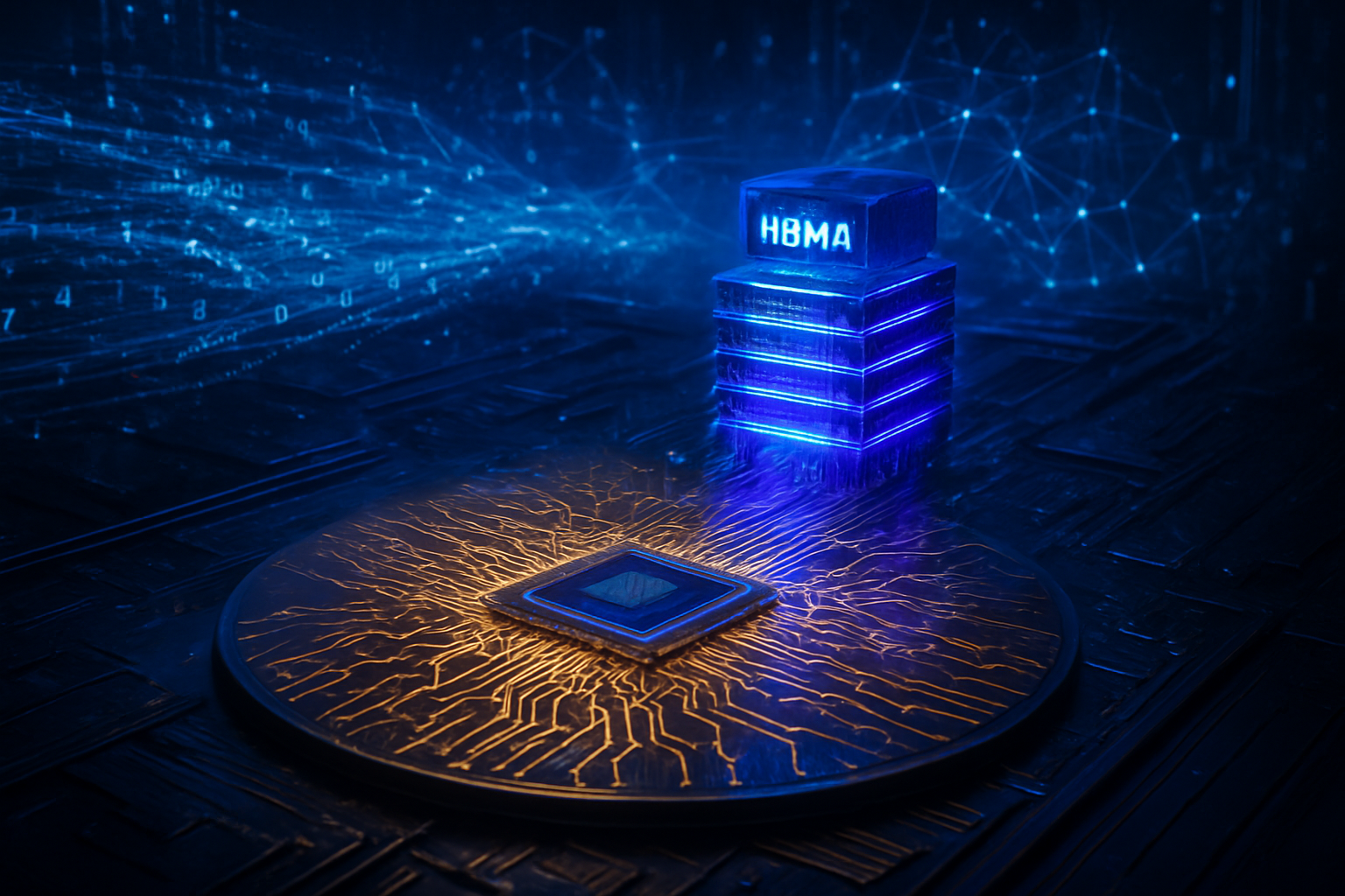
    The move toward advanced packaging is driven by two primary technical barriers: the reticle limit and the "memory wall." A single lithography step cannot print a die larger than approximately 858mm², yet the computational demands of AI training require far more surface area for logic and memory. To solve this, TSMC (NYSE: TSM) has pioneered "Ultra-Large CoWoS," which as of late 2025 allows for packages up to nine times the standard reticle size. By "stitching" multiple GPU dies together on a silicon interposer, manufacturers can create a unified processor that the software perceives as a single, massive chip. This is the foundation of the NVIDIA Rubin R100, which utilizes CoWoS-L packaging to integrate 12 stacks of HBM4 memory, providing a staggering 13 TB/s of memory bandwidth.

    Furthermore, the integration of High Bandwidth Memory (HBM4) has become the gold standard for 2025 AI hardware. Unlike traditional DDR memory, HBM4 is stacked vertically and placed microns away from the logic die using advanced interconnects. The current technical specifications for HBM4 include a 2,048-bit interface—double that of HBM3E—and bandwidth speeds reaching 2.0 TB/s per stack. This proximity is vital because it addresses the "memory wall," where the speed of the processor far outstrips the speed at which data can be delivered to it. By using "bumpless" bonding and hybrid bonding techniques, such as TSMC’s SoIC (System on Integrated Chips), engineers have achieved interconnect densities of over one million per square millimeter, reducing power consumption and latency to near-monolithic levels.

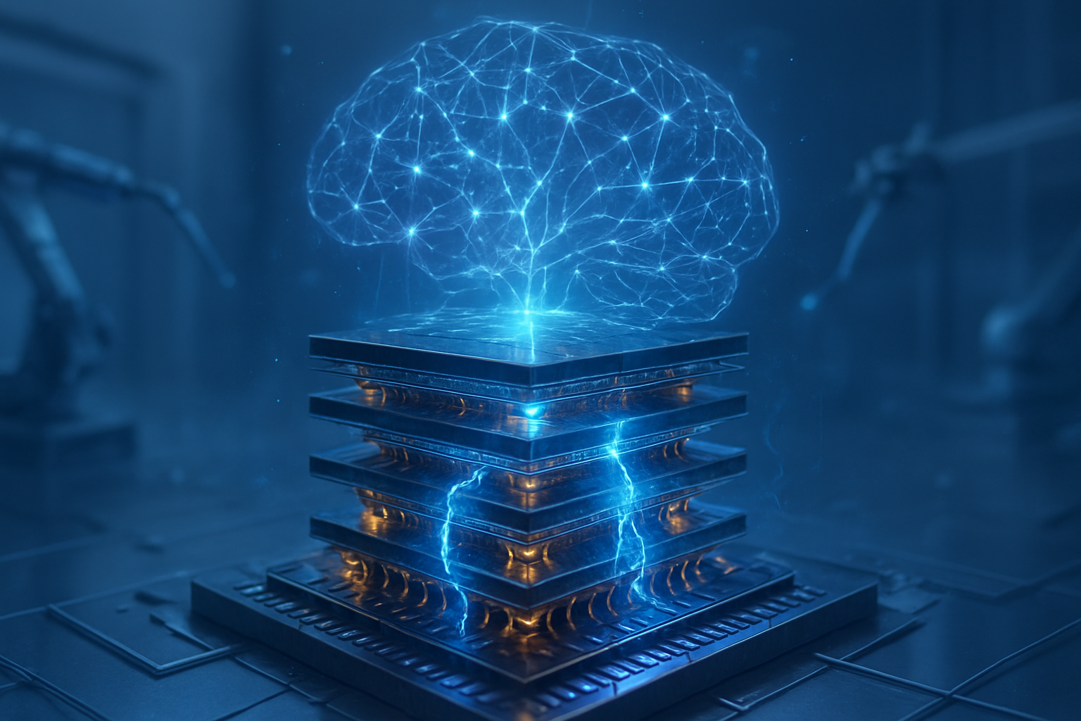
    Initial reactions from the AI research community have been overwhelmingly positive, as these packaging breakthroughs have enabled the training of models with tens of trillions of parameters. Industry experts note that without the transition to 3D stacking and chiplets, the power density of AI chips would have become unmanageable. The shift to heterogeneous integration—using the most expensive 2nm nodes only for critical compute cores while using mature 5nm nodes for I/O—has also allowed for better yield management, preventing the cost of AI hardware from spiraling even further out of control.

    The Competitive Landscape: Foundries Move Beyond the Wafer

    The battle for packaging supremacy has reshaped the competitive dynamics between the world’s leading foundries. TSMC (NYSE: TSM) remains the dominant force, having expanded its CoWoS capacity to an estimated 80,000 wafers per month by the end of 2025. Its new AP8 fab in Tainan is now fully operational, specifically designed to meet the insatiable demand from NVIDIA and AMD (NASDAQ: AMD). TSMC’s SoIC-X technology, which offers a 6μm bond pitch, is currently considered the industry benchmark for true 3D die stacking.

    However, Intel (NASDAQ: INTC) has emerged as a formidable challenger with its "IDM 2.0" strategy. Intel’s Foveros Direct 3D and EMIB (Embedded Multi-die Interconnect Bridge) technologies are now being produced in volume at its New Mexico facilities. This has allowed Intel to position itself as a "packaging-as-a-service" provider, attracting customers who want to diversify their supply chains away from Taiwan. In a major strategic win, Intel recently began mass-producing advanced interconnects for several "hyperscaler" firms that are designing their own custom AI silicon but lack the packaging infrastructure to assemble them.

    Samsung (KRX: 005930) is also making aggressive moves to bridge the gap. By late 2025, Samsung’s 2nm Gate-All-Around (GAA) process reached stable yields, and the company has successfully integrated its I-Cube and X-Cube packaging solutions for high-profile clients. A landmark deal was recently finalized where Samsung produces the front-end logic dies for Tesla’s (NASDAQ: TSLA) Dojo AI6, while the advanced packaging is handled in a "split-foundry" model involving Intel’s assembly lines. This level of cross-foundry collaboration was unheard of five years ago but has become a necessity in the complex 2025 ecosystem.

    The Wider Significance: A New Era of Heterogeneous Computing

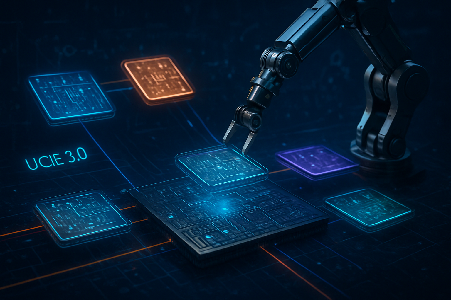
    This shift fits into a broader trend of "More than Moore," where performance gains are found through architectural ingenuity rather than just smaller transistors. As AI models become more specialized, the ability to mix and match chiplets from different vendors—using the Universal Chiplet Interconnect Express (UCIe) 3.0 standard—is becoming a reality. This allows a startup to pair a specialized AI accelerator chiplet with a standard I/O die from a major vendor, significantly lowering the barrier to entry for custom silicon.

    The impacts are profound: we are seeing a decoupling of logic scaling from memory scaling. However, this also raises concerns regarding thermal management. Packing so much computational power into such a small, 3D-stacked volume creates "hot spots" that traditional air cooling cannot handle. Consequently, the rise of advanced packaging has triggered a parallel boom in liquid cooling and immersion cooling technologies for data centers.

    Compared to previous milestones like the introduction of FinFET transistors, the packaging revolution is more about "system-level" efficiency. It acknowledges that the bottleneck is no longer how many calculations a chip can do, but how efficiently it can move data. This development is arguably the most critical factor in preventing an "AI winter" caused by hardware stagnation, ensuring that the infrastructure can keep pace with the rapidly evolving software side of the industry.

    Future Horizons: Toward "Bumpless" 3D Integration

    Looking ahead to 2026 and 2027, the industry is moving toward "bumpless" hybrid bonding as the standard for all flagship processors. This technology eliminates the tiny solder bumps currently used to connect dies, instead using direct copper-to-copper bonding. Experts predict this will lead to another 10x increase in interconnect density, effectively making a stack of chips perform as if they were a single piece of silicon. We are also seeing the early stages of optical interconnects, where light is used instead of electricity to move data between chiplets, potentially solving the heat and distance issues inherent in copper wiring.

    The next major challenge will be the "Power Wall." As chips consume upwards of 1,000 watts, delivering that power through the bottom of a 3D-stacked package is becoming nearly impossible. Research into backside power delivery—where power is routed through the back of the wafer rather than the top—is the next frontier that TSMC, Intel, and Samsung are all racing to perfect by 2026. If successful, this will allow for even denser packaging and higher clock speeds for AI training.

    Summary and Final Thoughts

    The transition from transistor-counting to advanced packaging marks the beginning of the "System-on-Package" era. TSMC’s dominance in CoWoS, Intel’s aggressive expansion of Foveros, and Samsung’s multi-foundry collaborations have turned the back-end of semiconductor manufacturing into the most strategic sector of the global tech economy. The key takeaway for 2025 is that the "chip" is no longer just a piece of silicon; it is a complex, multi-layered city of interconnects, memory stacks, and specialized logic.

    In the history of AI, this period will likely be remembered as the moment when hardware architecture finally caught up to the needs of neural networks. The long-term impact will be a democratization of custom silicon through chiplet standards like UCIe, even as the "Big Three" foundries consolidate their power over the physical assembly process. In the coming months, watch for the first "multi-vendor" chiplets to hit the market and for the escalation of the "packaging arms race" as foundries announce even larger multi-reticle designs to power the AI models of 2026.


    This content is intended for informational purposes only and represents analysis of current AI developments.

    TokenRing AI delivers enterprise-grade solutions for multi-agent AI workflow orchestration, AI-powered development tools, and seamless remote collaboration platforms.
    For more information, visit https://www.tokenring.ai/.

  • The Silicon Renaissance: US Fabs Go Online as CHIPS Act Shifts to Venture-Style Equity

    The Silicon Renaissance: US Fabs Go Online as CHIPS Act Shifts to Venture-Style Equity

    As of December 18, 2025, the landscape of American semiconductor manufacturing has transitioned from a series of ambitious legislative promises into a tangible, operational reality. The CHIPS and Science Act, once a theoretical framework for industrial policy, has reached a critical inflection point where the first "made-in-USA" advanced logic wafers are finally rolling off production lines in Arizona and Texas. This milestone marks the most significant shift in global hardware production in three decades, as the United States attempts to claw back its share of the leading-edge foundry market from Asian giants.

    The final quarter of 2025 has seen a dramatic evolution in how these domestic projects are managed. Following the establishment of the U.S. Investment Accelerator earlier this year, the federal government has pivoted from a traditional grant-based system to a "venture-capital style" model. This includes the high-profile finalization of a 9.9% equity stake in Intel (NASDAQ: INTC), funded through a combination of remaining CHIPS grants and the "Secure Enclave" program. By becoming a shareholder in its national champion, the U.S. government has signaled that domestic AI sovereignty is no longer just a matter of policy, but a direct national investment.

    High-Volume 18A and the Yield Challenge

    The technical centerpiece of this domestic resurgence is Intel’s 18A (1.8nm) process node, which officially entered high-volume mass production at Fab 52 in Chandler, Arizona, in October 2025. This node represents the first time a U.S. firm has attempted to leapfrog the industry leader, TSMC (NYSE: TSM), by utilizing RibbonFET Gate-All-Around (GAA) architecture and PowerVia backside power delivery ahead of its competitors. Initial internal products, including the "Panther Lake" AI PC processors and "Clearwater Forest" server chips, have successfully powered on, demonstrating that the architecture is functional. However, the technical transition has not been without friction; industry analysts report that 18A yields are currently in a "ramp-up phase," meaning they are predictable but not yet at the commercial efficiency levels seen in mature Taiwanese facilities.

    Meanwhile, TSMC’s Arizona Fab 1 has reached steady-state volume production, currently churning out 4nm and 5nm chips for major clients like Apple (NASDAQ: AAPL) and NVIDIA (NASDAQ: NVDA). This facility is already providing the essential "Blackwell" architecture components that power the latest generation of AI data centers. TSMC has also accelerated its timeline for Fab 2, with cleanroom equipment installation now targeting 3nm production by early 2027. This technical progress is bolstered by the deployment of the latest High-NA Extreme Ultraviolet (EUV) lithography machines, which are essential for printing the sub-2nm features required for the next generation of AI accelerators.

    The competitive gap is further complicated by Samsung (KRX: 005930), which has pivoted its Taylor, Texas facility to focus exclusively on 2nm production. While the project faced construction delays throughout 2024, the fab is now over 90% complete and is expected to go online in early 2026. A significant development this month was the deepening of the Samsung-Tesla (NASDAQ: TSLA) partnership, with Tesla engineers now occupying dedicated workspace within the Taylor fab to oversee the final qualification of the AI5 and AI6 chips. This "co-location" strategy represents a new technical paradigm where the chip designer and the foundry work in physical proximity to optimize silicon for specific AI workloads.

    The Competitive Landscape: Diversification vs. Dominance

    The immediate beneficiaries of this domestic capacity are the "fabless" giants who have long been vulnerable to the geopolitical risks of the Taiwan Strait. NVIDIA and AMD (NASDAQ: AMD) are the primary winners, as they can now claim a portion of their supply chain is "on-shored," satisfying both ESG requirements and federal procurement mandates. For NVIDIA, having a secondary source for Blackwell-class chips in Arizona provides a strategic buffer against potential disruptions in East Asia. Microsoft (NASDAQ: MSFT) has also emerged as a key strategic partner for Intel’s 18A node, utilizing the domestic capacity to manufacture its "Maia 2" AI processors, which are central to its Azure AI infrastructure.

    However, the competitive implications for major AI labs are nuanced. While the U.S. is adding capacity, TSMC’s home-base operations in Taiwan remain the "gold standard" for yield and cost-efficiency. In late 2025, TSMC Taiwan successfully commenced volume production of its N2 (2nm) node with yields exceeding 70%, a figure that Intel and Samsung are still struggling to match in their U.S. facilities. This creates a two-tiered market: the most cutting-edge, cost-effective silicon still flows from Taiwan, while the U.S. fabs serve as a high-security, "sovereign" alternative for mission-critical and government-adjacent AI applications.

    The disruption to existing services is most visible in the automotive and industrial sectors. With the U.S. government now holding equity in domestic foundries, there is increasing pressure for "Buy American" mandates in federal AI contracts. This has forced startups and mid-sized AI firms to re-evaluate their hardware roadmaps, often choosing slightly more expensive domestic-made chips to ensure long-term regulatory compliance. The strategic advantage has shifted from those who have the best design to those who have guaranteed "wafer starts" on American soil, a commodity that remains in high demand and limited supply.

    Geopolitical Friction and the Asian Response

    The broader significance of the CHIPS Act's 2025 status cannot be overstated; it represents a decoupling of the AI hardware stack that was unthinkable five years ago. This development fits into a larger trend of "techno-nationalism," where computing power is viewed as a strategic resource akin to oil. However, this shift has prompted a fierce response from Asian foundries. In China, SMIC (HKG: 0981) has defied expectations by reaching volume production on its "N+3" 5nm-equivalent node without the use of EUV machines. While their costs are significantly higher and yields lower, the successful release of the Huawei Mate 80 series in late 2025 proves that the U.S. lead in manufacturing is not an absolute barrier to entry.

    Furthermore, Japan’s Rapidus has emerged as a formidable "third way" in the semiconductor wars. By successfully launching a 2nm pilot line in Hokkaido this year through an alliance with IBM (NYSE: IBM), Japan is positioning itself to leapfrog the 3nm generation entirely. This highlights a potential concern for the U.S. strategy: while the CHIPS Act has successfully brought manufacturing back to American shores, it has also sparked a global subsidy race. The U.S. now finds itself competing not just with rivals like China, but with allies like Japan and South Korea, who are equally determined to maintain their technological relevance in the AI era.

    Comparisons to previous milestones, such as the 1980s semiconductor trade disputes, suggest that we are entering a decade of sustained government intervention in the hardware market. The shift toward equity stakes in companies like Intel suggests that the "free market" era of chip manufacturing is effectively over. The potential concern for the AI industry is that this fragmentation could lead to higher hardware costs and slower innovation cycles as companies navigate a "patchwork" of regional manufacturing requirements rather than a single, globalized supply chain.

    The Road to 1nm and the 2030 Horizon

    Looking ahead, the next two years will be defined by the race to 1nm and the implementation of "High-NA" EUV technology across all major US sites. Intel’s success or failure in stabilizing 18A yields by mid-2026 will determine if the U.S. can truly claim technical parity with TSMC. If yields improve, we expect to see a surge in external foundry customers moving away from "Taiwan-only" strategies. Conversely, if yields remain low, the U.S. government may be forced to increase its equity stakes or provide further "bridge funding" to prevent its national champions from falling behind.

    Near-term developments also include the expansion of advanced packaging facilities. While the CHIPS Act focused heavily on "front-end" wafer fabrication, the "back-end" packaging of AI chips remains a bottleneck. We expect the next round of funding to focus heavily on domestic CoWoS (Chip-on-Wafer-on-Substrate) equivalents to ensure that chips made in Arizona don't have to be sent back to Asia for final assembly. Experts predict that by 2030, the U.S. could account for 20% of global leading-edge production, up from 0% in 2022, provided that the labor shortage in specialized engineering is addressed through updated immigration and education policies.

    A New Era for American Silicon

    The CHIPS Act update of late 2025 reveals a landscape that is both promising and precarious. The key takeaway is that the "brick and mortar" phase of the U.S. semiconductor resurgence is complete; the factories are built, the machines are humming, and the first chips are in hand. However, the transition from building factories to running them at world-class efficiency is a challenge that money alone cannot solve. The U.S. has successfully bought its way back into the game, but winning the game will require a sustained commitment to yield optimization and workforce development.

    In the history of AI, this period will likely be remembered as the moment when the "cloud" was anchored to the ground. The physical infrastructure of AI—the silicon, the power, and the packaging—is being redistributed across the globe, ending the era of extreme geographic concentration. As we move into 2026, the industry will be watching the quarterly yield reports from Arizona and the progress of Samsung’s 2nm pivot in Texas. The silicon renaissance has begun, but the true test of its endurance lies in the wafers that will be etched in the coming months.


    This content is intended for informational purposes only and represents analysis of current AI developments.

    TokenRing AI delivers enterprise-grade solutions for multi-agent AI workflow orchestration, AI-powered development tools, and seamless remote collaboration platforms.
    For more information, visit https://www.tokenring.ai/.

  • The Green Paradox: How Semiconductor Giants are Racing to Decarbonize the AI Boom

    The Green Paradox: How Semiconductor Giants are Racing to Decarbonize the AI Boom

    As the calendar turns to late 2025, the semiconductor industry finds itself at a historic crossroads. The global insatiable demand for high-performance AI hardware has triggered an unprecedented manufacturing expansion, yet this growth is colliding head-on with the most ambitious sustainability targets in industrial history. Major foundries are now forced to navigate a "green paradox": while the chips they produce are becoming more energy-efficient, the sheer scale of production required to power the world’s generative AI models is driving absolute energy and water consumption to record highs.

    To meet this challenge, the industry's titans—Taiwan Semiconductor Manufacturing Co. (NYSE:TSM), Intel (Nasdaq:INTC), and Samsung Electronics (KRX:005930)—have moved beyond mere corporate social responsibility. In 2025, sustainability has become a core competitive metric, as vital as transistor density or clock speed. From massive industrial water reclamation plants in the Arizona desert to AI-driven "digital twin" factories in South Korea, the race is on to prove that the silicon backbone of the future can be both high-performance and environmentally sustainable.

    The High-NA Energy Trade-off and Technical Innovations

    The technical centerpiece of 2025's manufacturing landscape is the High-NA (High Numerical Aperture) EUV lithography system, primarily supplied by ASML (Nasdaq:ASML). These machines, such as the EXE:5200 series, are the most complex tools ever built, but they come with a significant environmental footprint. A single High-NA EUV tool now consumes approximately 1.4 Megawatts (MW) of power—a 20% increase over standard EUV systems. However, foundries argue that this is a net win for sustainability. By enabling "single-exposure" lithography for the 2nm and 1.4nm nodes, these tools eliminate the need for 3–4 multi-patterning steps required by older machines, effectively saving an estimated 200 kWh per wafer produced.

    Beyond lithography, water management has seen a radical technical overhaul. TSMC (NYSE:TSM) recently reached a major milestone with the groundbreaking of its Arizona Industrial Reclamation Water Plant (IRWP). This 15-acre facility is designed to achieve a 90% water recycling rate for its US operations by 2028. Similarly, in Taiwan, the Rende Reclaimed Water Plant became fully operational this year, providing a critical lifeline to the Tainan Science Park’s 3nm and 2nm lines. These facilities use advanced membrane bioreactors and reverse osmosis systems to ensure that every gallon of water is reused multiple times before being safely returned to the environment.

    Samsung (KRX:005930) has taken a different technical route by applying AI to the manufacturing of AI chips. In a landmark partnership with NVIDIA (Nasdaq:NVDA), Samsung has deployed "Digital Twin" technology across its Hwaseong and Pyeongtaek campuses. By creating a real-time virtual replica of the entire fab, Samsung uses over 50,000 GPUs to simulate and optimize airflow, chemical distribution, and power consumption. Early data from late 2025 suggests this AI-driven management has improved operational energy efficiency by nearly 20 times compared to legacy manual systems, demonstrating a circular logic where AI is the primary tool used to mitigate its own environmental impact.

    Market Positioning: The Rise of the "Sustainable Foundry"

    Sustainability has shifted from a line item in an annual report to a strategic advantage in foundry contract negotiations. Intel (Nasdaq:INTC) has positioned itself as the industry's sustainability leader, marketing its "Intel 18A" node not just on performance, but as the world’s most "sustainable advanced node." By late 2025, Intel maintained a 99% renewable electricity rate across its global operations and achieved a "Net Positive Water" status in key regions like Oregon, where it has restored over 10 billion cumulative gallons to local watersheds. This allows Intel to pitch itself to climate-conscious tech giants who are under pressure to reduce their Scope 3 emissions.

    The competitive implications are stark. As cloud providers like Microsoft, Google, and Amazon strive for carbon neutrality, they are increasingly scrutinizing the carbon footprint of the chips in their data centers. TSMC (NYSE:TSM) has responded by accelerating its RE100 timeline, now aiming for 100% renewable energy by 2040—a full decade ahead of its original 2050 target. TSMC is also leveraging its market dominance to enforce "Green Agreements" with over 50 of its tier-1 suppliers, essentially mandating carbon reductions across the entire semiconductor supply chain to ensure its chips remain the preferred choice for the world’s largest tech companies.

    For startups and smaller AI labs, this shift is creating a new hierarchy of hardware. "Green Silicon" is becoming a premium tier of the market. While the initial CapEx for these sustainable fabs is enormous—with the industry spending over $160 billion in 2025 alone—the long-term operational savings from reduced water and energy waste are expected to stabilize chip prices in an era of rising resource costs. Companies that fail to adapt to these ESG requirements risk being locked out of high-value government contracts and the supply chains of the world’s largest consumer electronics brands.

    Global Significance and the Path to Net-Zero

    The broader significance of these developments cannot be overstated. The semiconductor industry's energy transition is a microcosm of the global challenge to decarbonize heavy industry. In Taiwan, TSMC’s energy footprint is projected to account for 12.5% of the island’s total power consumption by the end of 2025. This has turned semiconductor sustainability into a matter of national security and regional stability. The ability of foundries to integrate massive amounts of renewable energy—often through dedicated offshore wind farms and solar arrays—is now a prerequisite for obtaining the permits needed to build new multi-billion dollar "mega-fabs."

    However, concerns remain regarding the "carbon spike" associated with the construction of these new facilities. While the operational phase of a fab is becoming greener, the embodied carbon in the concrete, steel, and advanced machinery required for 18 new major fab projects globally in 2025 is substantial. Industry experts are closely watching whether the efficiency gains of the 2nm and 1.4nm nodes will be enough to offset the sheer volume of production. If AI demand continues its exponential trajectory, even a 90% recycling rate may not be enough to prevent a net increase in resource withdrawal.

    Comparatively, this era represents a shift from "Scaling at any Cost" to "Responsible Scaling." Much like the transition from leaded to unleaded gasoline or the adoption of scrubbers in the shipping industry, the semiconductor world is undergoing a fundamental re-engineering of its core processes. The move toward a "Circular Economy"—where Samsung (KRX:005930) now uses 31% recycled plastic in its components and all major foundries upcycle over 60% of their manufacturing waste—marks a transition toward a more mature, resilient industrial base.

    Future Horizons: The Road to 14A and Beyond

    Looking ahead to 2026 and beyond, the industry is already preparing for the next leap in sustainable manufacturing. Intel’s (Nasdaq:INTC) 14A roadmap and TSMC’s (NYSE:TSM) A16 node are being designed with "sustainability-first" architectures. This includes the wider adoption of Backside Power Delivery, which not only improves performance but also reduces the energy lost as heat within the chip itself. We also expect to see the first "Zero-Waste" fabs, where nearly 100% of chemicals and water are processed and reused on-site, effectively decoupling semiconductor production from local environmental constraints.

    The next frontier will be the integration of small-scale nuclear power, specifically Small Modular Reactors (SMRs), to provide consistent, carbon-free baseload power to mega-fabs. While still in the pilot phase in late 2025, several foundries have begun feasibility studies to co-locate SMRs with their newest manufacturing hubs. Challenges remain, particularly in the decarbonization of the "last mile" of the supply chain and the sourcing of rare earth minerals, but the momentum toward a truly green silicon shield is now irreversible.

    Summary and Final Thoughts

    The semiconductor industry’s journey in 2025 has proven that environmental stewardship and technological advancement are no longer mutually exclusive. Through massive investments in water reclamation, the adoption of High-NA EUV for process efficiency, and the use of AI to optimize the very factories that create it, the world's leading foundries are setting a new standard for industrial sustainability.

    Key takeaways from this year include:

    • Intel (Nasdaq:INTC) leading on renewable energy and water restoration.
    • TSMC (NYSE:TSM) accelerating its RE100 goals to 2040 to meet client demand.
    • Samsung (KRX:005930) pioneering AI-driven digital twins to slash operational waste.
    • ASML (Nasdaq:ASML) providing the High-NA tools that, while power-hungry, simplify manufacturing to save energy per wafer.

    In the coming months, watch for the first production yields from the 2nm nodes and the subsequent environmental audits. These reports will be the ultimate litmus test for whether the "Green Paradox" has been solved or if the AI boom will require even more radical interventions to protect our planet's resources.


    This content is intended for informational purposes only and represents analysis of current AI developments.

    TokenRing AI delivers enterprise-grade solutions for multi-agent AI workflow orchestration, AI-powered development tools, and seamless remote collaboration platforms.
    For more information, visit https://www.tokenring.ai/.

  • The High-NA Frontier: ASML Solidifies the Sub-2nm Era as EUV Adoption Hits Critical Mass

    The High-NA Frontier: ASML Solidifies the Sub-2nm Era as EUV Adoption Hits Critical Mass

    As of late 2025, the semiconductor industry has reached a historic inflection point, driven by the successful transition of High-Numerical Aperture (High-NA) Extreme Ultraviolet (EUV) lithography from experimental labs to the factory floor. ASML (NASDAQ: ASML), the world’s sole provider of the machinery required to print the world’s most advanced chips, has officially entered the high-volume manufacturing (HVM) phase for its next-generation systems. This milestone marks the beginning of the sub-2nm era, providing the essential infrastructure for the next decade of artificial intelligence, high-performance computing, and mobile technology.

    The immediate significance of this development cannot be overstated. With the shipment of the Twinscan EXE:5200B to major foundries, the industry has solved the "stitching" and throughput challenges that once threatened to stall Moore’s Law. For ASML, the successful ramp of these multi-hundred-million-dollar machines is the primary engine behind its projected 2030 revenue targets of up to €60 billion. As logic and DRAM manufacturers race to integrate these tools, the gap between those who can afford the "bleeding edge" and those who cannot has never been wider.

    Breaking the Sub-2nm Barrier: The Technical Triumph of High-NA

    The technical centerpiece of ASML’s 2025 success is the EXE:5200B, a machine that represents the pinnacle of human engineering. Unlike standard EUV tools, which use a 0.33 Numerical Aperture (NA) lens, High-NA systems utilize a 0.55 NA anamorphic lens system. This allows for a significantly higher resolution, enabling chipmakers to print features as small as 8nm—a requirement for the 1.4nm (A14) and 1nm nodes. By late 2025, ASML has successfully boosted the throughput of these systems to 175–200 wafers per hour (wph), matching the productivity of previous generations while drastically reducing the need for "multi-patterning."

    One of the most significant technical hurdles overcome this year was "reticle stitching." Because High-NA lenses are anamorphic (magnifying differently in the X and Y directions), the field size is halved compared to standard EUV. This required engineers to "stitch" two halves of a chip design together with nanometer precision. Reports from IMEC and Intel (NASDAQ: INTC) in mid-2025 confirmed that this process has stabilized, allowing for the production of massive AI accelerators that exceed traditional size limits. Furthermore, the industry has begun transitioning to Metal Oxide Resists (MOR), which are thinner and more sensitive than traditional chemically amplified resists, allowing the High-NA light to be captured more effectively.

    Initial reactions from the research community have been overwhelmingly positive, with experts noting that High-NA reduces the number of process steps by over 40 on critical layers. This reduction in complexity is vital for yield management at the 1.4nm node. While the sheer cost of the machines—estimated at over $380 million each—initially caused hesitation, the data from 2025 pilot lines has proven that the reduction in mask sets and processing time makes High-NA a cost-effective solution for the highest-volume, highest-performance chips.

    The Foundry Arms Race: Intel, TSMC, and Samsung Diverge

    The adoption of High-NA has created a strategic divide among the "Big Three" chipmakers. Intel has emerged as the most aggressive pioneer, having fully installed two production-grade EXE:5200 units at its Oregon facility by late 2025. Intel is betting its entire "Intel 14A" roadmap on being the first to market with High-NA, aiming to reclaim the crown of process leadership from TSMC (NYSE: TSM). For Intel, the strategic advantage lies in early mastery of the tool’s quirks, potentially allowing them to offer 1.4nm capacity to external foundry customers before their rivals.

    TSMC, conversely, has maintained a pragmatic stance for much of 2025, focusing on its N2 and A16 nodes using standard EUV with multi-patterning. However, the tide shifted in late 2025 when reports surfaced that TSMC had placed significant orders for High-NA machines to support its A14P node, expected to ramp in 2027-2028. This move signals that even the most cost-conscious foundry leader recognizes that standard EUV cannot scale indefinitely. Samsung (KRX: 005930) also took delivery of its first production High-NA unit in Q4 2025, intending to use the technology for its SF1.4 node to close the performance gap in the mobile and AI markets.

    The implications for the broader market are profound. Companies like NVIDIA (NASDAQ: NVDA) and Apple (NASDAQ: AAPL) are now forced to navigate this fragmented landscape, deciding whether to stick with TSMC’s proven 0.33 NA methods or pivot to Intel’s High-NA-first approach for their next-generation AI GPUs and silicon. This competition is driving a "supercycle" for ASML, as every major player is forced to buy the most expensive equipment just to stay in the race, further cementing ASML’s monopoly at the top of the supply chain.

    Beyond Logic: EUV’s Critical Role in DRAM and Global Trends

    While logic manufacturing often grabs the headlines, 2025 has been the year EUV became indispensable for memory. The mass production of "1c" (12nm-class) DRAM is now in full swing, with SK Hynix (KRX: 000660) leading the charge by utilizing five to six EUV layers for its HBM4 (High Bandwidth Memory) products. Even Micron (NASDAQ: MU), which was famously the last major holdout for EUV technology, has successfully ramped its 1-gamma node using EUV at its Hiroshima plant this year. The integration of EUV in DRAM is critical for ASML’s long-term margins, as memory manufacturers typically purchase tools in higher volumes than logic foundries.

    This shift fits into a broader global trend: the AI Supercycle. The explosion in demand for generative AI has created a bottomless appetite for high-density memory and high-performance logic, both of which now require EUV. However, this growth is occurring against a backdrop of geopolitical complexity. ASML has reported that while demand from China has normalized—dropping to roughly 20% of revenue from nearly 50% in 2024 due to export restrictions—the global demand for advanced tools has more than compensated. ASML’s gross margin targets of 56% to 60% by 2030 are predicated on this shift toward higher-value High-NA systems and the expansion of EUV into the memory sector.

    Comparisons to previous milestones, such as the initial move from DUV to EUV in 2018, suggest that we are entering a "harvesting" phase. The foundational science is settled, and the focus has shifted to industrialization and yield optimization. The potential concern remains the "cost wall"—the risk that only a handful of companies can afford to design chips at the 1.4nm level, potentially centralizing the AI industry even further into the hands of a few tech giants.

    The Roadmap to 2030: From High-NA to Hyper-NA

    Looking ahead, ASML is already laying the groundwork for the next decade with "Hyper-NA" lithography. As High-NA carries the industry through the 1.4nm and 1nm eras, the subsequent generation of transistors—likely based on Complementary FET (CFET) architectures—will require even higher resolution. ASML’s roadmap for the HXE series targets a 0.75 NA, which would be the most significant jump in optical capability in the company's history. Pilot systems for Hyper-NA are currently projected for introduction around 2030.

    The challenges for Hyper-NA are daunting. At 0.75 NA, the depth of focus becomes extremely shallow, and light polarization effects can degrade image contrast. ASML is currently researching specialized polarization filters and even more advanced photoresist materials to combat these physics-based limitations. Experts predict that the move to Hyper-NA will be as difficult as the original transition to EUV, requiring a complete overhaul of the mask and pellicle ecosystem. However, if successful, it will extend the life of silicon-based computing well into the 2030s.

    In the near term, the industry will focus on the "A14" ramp. We expect to see the first silicon samples from Intel’s High-NA lines by mid-2026, which will be the ultimate test of whether the technology can deliver on its promise of superior power, performance, and area (PPA). If Intel succeeds in hitting its yield targets, it could trigger a massive wave of "FOMO" (fear of missing out) among other chipmakers, leading to an even faster adoption rate for ASML’s most advanced tools.

    Conclusion: The Indispensable Backbone of AI

    The status of ASML and EUV lithography at the end of 2025 confirms one undeniable truth: the future of artificial intelligence is physically etched by a single company in Veldhoven. The successful deployment of High-NA lithography has effectively moved the goalposts for Moore’s Law, ensuring that the roadmap to sub-2nm chips is not just a theoretical possibility but a manufacturing reality. ASML’s ability to maintain its technological lead while expanding its margins through logic and DRAM adoption has solidified its position as the most critical node in the global technology supply chain.

    As we move into 2026, the industry will be watching for the first "High-NA chips" to enter the market. The success of these products will determine the pace of the next decade of computing. For now, ASML has proven that it can meet the moment, providing the tools necessary to build the increasingly complex brains of the AI era. The "High-NA Era" has officially arrived, and with it, a new chapter in the history of human innovation.


    This content is intended for informational purposes only and represents analysis of current AI developments.

    TokenRing AI delivers enterprise-grade solutions for multi-agent AI workflow orchestration, AI-powered development tools, and seamless remote collaboration platforms.
    For more information, visit https://www.tokenring.ai/.

  • The Great Unbundling of Silicon: How UCIe 3.0 is Powering a New Era of ‘Mix-and-Match’ AI Hardware

    The Great Unbundling of Silicon: How UCIe 3.0 is Powering a New Era of ‘Mix-and-Match’ AI Hardware

    The semiconductor industry has reached a pivotal turning point as the Universal Chiplet Interconnect Express (UCIe) standard enters full commercial maturity. As of late 2025, the release of the UCIe 3.0 specification has effectively dismantled the era of monolithic, "black box" processors, replacing it with a modular "mix and match" ecosystem. This development allows specialized silicon components—known as chiplets—from different manufacturers to be housed within a single package, communicating at speeds that were previously only possible within a single piece of silicon. For the artificial intelligence sector, this represents a massive leap forward, enabling the construction of hyper-specialized AI accelerators that can scale to meet the insatiable compute demands of next-generation large language models (LLMs).

    The immediate significance of this transition cannot be overstated. By standardizing how these chiplets communicate, the industry is moving away from proprietary, vendor-locked architectures toward an open marketplace. This shift is expected to slash development costs for custom AI silicon by up to 40% and reduce time-to-market by nearly a year for many fabless design firms. As the AI hardware race intensifies, UCIe 3.0 provides the "lingua franca" that ensures an I/O die from one vendor can work seamlessly with a compute engine from another, all while maintaining the ultra-low latency required for real-time AI inference and training.

    The Technical Backbone: From UCIe 1.1 to the 64 GT/s Breakthrough

    The technical evolution of the UCIe standard has been rapid, culminating in the August 2025 release of the UCIe 3.0 specification. While UCIe 1.1 focused on basic reliability and health monitoring for automotive and data center applications, and UCIe 2.0 introduced standardized manageability and 3D packaging support, the 3.0 update is a game-changer for high-performance computing. It doubles the data rate to 64 GT/s per lane, providing the massive throughput necessary for the "XPU-to-memory" bottlenecks that have plagued AI clusters. A key innovation in the 3.0 spec is "Runtime Recalibration," which allows links to dynamically adjust power and performance without requiring a system reboot—a critical feature for massive AI data centers that must remain operational 24/7.

    This new standard differs fundamentally from previous approaches like Intel Corporation (NASDAQ: INTC)’s proprietary Advanced Interface Bus (AIB) or Advanced Micro Devices, Inc. (NASDAQ: AMD)’s early Infinity Fabric. While those technologies proved the viability of chiplets, they were "closed loops" that prevented cross-vendor interoperability. UCIe 3.0, by contrast, defines everything from the physical layer (the actual wires and bumps) to the protocol layer, ensuring that a chiplet designed by a startup can be integrated into a larger system-on-chip (SoC) manufactured by a giant like NVIDIA Corporation (NASDAQ: NVDA). Initial reactions from the research community have been overwhelmingly positive, with engineers at the Open Compute Project (OCP) hailing it as the "PCIe moment" for internal chip communication.

    The Competitive Landscape: Giants and Challengers Align

    The shift toward a standardized chiplet ecosystem is creating a new hierarchy among tech giants. Intel Corporation (NASDAQ: INTC) has been the most aggressive proponent, having donated the initial specification to the consortium. Their recent launch of the Granite Rapids-D (Xeon 6 SoC) in early 2025 stands as one of the first high-volume products to fully leverage UCIe for modularity at the edge. Meanwhile, NVIDIA Corporation (NASDAQ: NVDA) has adapted its strategy; while it still champions its proprietary NVLink for high-end GPU clusters, it recently released "UCIe-ready" silicon bridges. These bridges allow customers to build custom AI accelerators that can talk directly to NVIDIA’s Blackwell and upcoming Rubin architectures, effectively turning NVIDIA’s hardware into a platform for third-party innovation.

    Taiwan Semiconductor Manufacturing Company (NYSE: TSM) and Samsung Electronics (KRX: 005930) are currently locked in a "foundry race" to provide the packaging technology that makes UCIe possible. TSMC’s 3DFabric and Samsung’s I-Cube/X-Cube technologies are the physical stages where these mix-and-match chiplets perform. In mid-2025, Samsung successfully demonstrated a 4nm chiplet prototype using IP from Synopsys, Inc. (NASDAQ: SNPS), proving that the "mix and match" dream is now a physical reality. This benefits smaller AI startups and fabless companies, who can now purchase "silicon-proven" UCIe blocks from providers like Cadence Design Systems, Inc. (NASDAQ: CDNS) instead of spending millions to design proprietary interconnect logic from scratch.

    Scaling AI: Efficiency, Cost, and the End of the "Reticle Limit"

    The broader significance of UCIe 3.0 lies in its ability to bypass the "reticle limit"—the physical size limit of a single silicon wafer die. As AI models grow, the chips needed to train them have become so large they are physically impossible to manufacture as a single piece of silicon without massive defects. By breaking the processor into smaller chiplets, manufacturers can achieve much higher yields and lower costs. This fits into the broader AI trend of "heterogeneous computing," where different parts of an AI task are handled by specialized hardware—such as a dedicated matrix multiplication die paired with a high-bandwidth memory (HBM) die and a low-power I/O die.

    However, this transition is not without concerns. The primary challenge remains "Standardized Manageability"—the difficulty of debugging a system when the components come from five different companies. If an AI server fails, determining which vendor’s chiplet caused the error becomes a complex legal and technical nightmare. Furthermore, while UCIe 3.0 provides the physical connection, the software stack required to manage these disparate components is still in its infancy. Despite these hurdles, the move toward UCIe is being compared to the transition from mainframe computers to modular PCs; it is an "unbundling" that democratizes high-performance silicon.

    The Horizon: Optical I/O and the 'Chiplet Store'

    Looking ahead, the near-term focus will be on the integration of Optical Compute Interconnects (OCI). Intel has already demonstrated a fully integrated optical I/O chiplet using UCIe that allows chiplets to communicate via fiber optics at 4TBps over distances up to 100 meters. This effectively turns an entire data center rack into a single, giant "virtual chip." In the long term, experts predict the rise of the "Chiplet Store"—a commercial marketplace where companies can buy pre-manufactured, specialized AI chiplets (like a dedicated "Transformer Engine" or a "Security Enclave") and have them assembled by a third-party packaging house.

    The challenges that remain are primarily thermal and structural. Stacking chiplets in 3D (as supported by UCIe 2.0 and 3.0) creates intense heat pockets that require advanced liquid cooling or new materials like glass substrates. Industry analysts predict that by 2027, more than 80% of all high-end AI processors will be UCIe-compliant, as the cost of maintaining proprietary interconnects becomes unsustainable even for the largest tech companies.

    A New Blueprint for the AI Age

    The maturation of the UCIe standard represents one of the most significant architectural shifts in the history of computing. By providing a standardized, high-speed interface for chiplets, the industry has unlocked a modular future that balances the need for extreme performance with the economic realities of semiconductor manufacturing. The "mix and match" ecosystem is no longer a theoretical concept; it is the foundation upon which the next decade of AI progress will be built.

    As we move into 2026, the industry will be watching for the first "multi-vendor" AI chips to hit the market—processors where the compute, memory, and I/O are sourced from entirely different companies. This development marks the end of the monolithic era and the beginning of a more collaborative, efficient, and innovative period in silicon design. For AI companies and investors alike, the message is clear: the future of hardware is no longer about who can build the biggest chip, but who can best orchestrate the most efficient ecosystem of chiplets.


    This content is intended for informational purposes only and represents analysis of current AI developments.

    TokenRing AI delivers enterprise-grade solutions for multi-agent AI workflow orchestration, AI-powered development tools, and seamless remote collaboration platforms.
    For more information, visit https://www.tokenring.ai/.

  • The Silicon Renaissance: US Mega-Fabs Enter Operational Phase as CHIPS Act Reshapes Global AI Power

    The Silicon Renaissance: US Mega-Fabs Enter Operational Phase as CHIPS Act Reshapes Global AI Power

    As of December 18, 2025, the landscape of global technology has reached a historic inflection point. What began three years ago as a legislative ambition to reshore semiconductor manufacturing has manifested into a sprawling industrial reality across the American Sun Belt and Midwest. The implementation of the CHIPS and Science Act has moved beyond the era of press releases and groundbreaking ceremonies into a high-stakes operational phase, defined by the rise of "Mega-Fabs"—massive, multi-billion dollar complexes designed to secure the hardware foundation of the artificial intelligence revolution.

    This transition marks a fundamental shift in the geopolitical order of technology. For the first time in decades, the most advanced logic chips required for generative AI and autonomous systems are being etched onto silicon in Arizona and Ohio. However, the road to "Silicon Sovereignty" has been paved with unexpected policy pivots, including a controversial move by the U.S. government to take equity stakes in domestic champions, and a fierce race between Intel, TSMC, and Samsung to dominate the 2-nanometer (2nm) frontier on American soil.

    The Technical Frontier: 2nm Targets and High-NA EUV Integration

    The technical execution of these Mega-Fabs has become a litmus test for the next generation of computing. Intel (NASDAQ: INTC) has achieved a significant milestone at its Fab 52 in Arizona, which has officially commenced limited mass production of its 18A node (approximately 1.8nm equivalent). This node utilizes RibbonFET gate-all-around (GAA) architecture and PowerVia backside power delivery—technologies that Intel claims will provide a definitive lead over competitors in power efficiency. Meanwhile, Intel’s "Silicon Heartland" project in New Albany, Ohio, has faced structural delays, pushing its full operational status to 2030. To compensate, the Ohio site is now being outfitted with "High-NA" (High Numerical Aperture) Extreme Ultraviolet (EUV) lithography machines from ASML, skipping older generations to debut with post-14A nodes.

    TSMC (NYSE: TSM) continues to set the gold standard for operational efficiency in the U.S. Their Phoenix, Arizona, Fab 1 is currently in full high-volume production of 4nm chips, with yields reportedly matching those of its Taiwanese facilities—a feat many analysts thought impossible two years ago. In response to insatiable demand from AI giants, TSMC has accelerated the timeline for its third Arizona fab. Originally slated for the end of the decade, Fab 3 is now being fast-tracked to produce 2nm (N2) and A16 nodes by late 2028. This facility will be the first in the U.S. to utilize TSMC’s sophisticated nanosheet transistor structures at scale.

    Samsung (KRX: 005930) has taken a high-risk, high-reward approach in Taylor, Texas. After facing initial delays due to a lack of "anchor customers" for 4nm production, the South Korean giant recalibrated its strategy to skip directly to 2nm production for the site's 2026 opening. By focusing on 2nm from day one, Samsung aims to undercut TSMC on wafer pricing, targeting a cost of $20,000 per wafer compared to TSMC’s projected $30,000. This aggressive technical pivot is designed to lure AI chip designers who are looking for a domestic alternative to the TSMC monopoly.

    Market Disruptions and the New "Equity for Subsidies" Model

    The business of semiconductors has been transformed by a new "America First" industrial policy. In a landmark move in August 2025, the U.S. Department of Commerce finalized a deal to take a 9.9% equity stake in Intel (NASDAQ: INTC) in exchange for $8.9 billion in combined CHIPS Act grants and "Secure Enclave" funding. This "Equity for Subsidies" model has sent ripples through Wall Street, signaling that the U.S. government is no longer just a regulator or a customer, but a shareholder in the nation's foundry future. This move has stabilized Intel’s balance sheet during its massive Ohio expansion but has raised questions about long-term government interference in corporate strategy.

    For the primary consumers of these chips—NVIDIA (NASDAQ: NVDA), Apple (NASDAQ: AAPL), and AMD (NASDAQ: AMD)—the rise of domestic Mega-Fabs offers a strategic hedge against geopolitical instability in the Taiwan Strait. However, the transition is not without cost. While domestic production reduces the risk of supply chain decapitation, the "Silicon Renaissance" is proving expensive. Analysts estimate that chips produced in U.S. Mega-Fabs carry a 20% to 30% "reshoring premium" due to higher labor and energy costs. NVIDIA and Apple have already begun signaling that these costs will likely be passed down to enterprise customers in the form of higher prices for AI accelerators and high-end consumer hardware.

    The competitive landscape is also being reshaped by the "Trump Royalty"—a policy involving government-managed cuts on high-end AI chip exports. This has forced companies like NVIDIA to navigate a complex web of "managed access" for international sales, further incentivizing the use of U.S.-based fabs to ensure compliance with tightening national security mandates. The result is a bifurcated market where "Made in USA" silicon becomes the premium standard for security-cleared and high-performance AI applications.

    Sovereignty, Bottlenecks, and the Global AI Landscape

    The broader significance of the Mega-Fab era lies in the pursuit of AI sovereignty. As AI models become the primary engine of economic growth, the physical infrastructure that powers them has become a matter of national survival. The CHIPS Act implementation has successfully broken the 100% reliance on East Asian foundries for leading-edge logic. However, a critical vulnerability remains: the "Packaging Bottleneck." Despite the progress in fabrication, the majority of U.S.-made wafers must still be shipped to Taiwan or Southeast Asia for advanced packaging (CoWoS), which is essential for binding logic and memory into a single AI super-chip.

    Furthermore, the industry has identified a secondary crisis in High-Bandwidth Memory (HBM). While Intel and TSMC are building the "brains" of AI in the U.S., the "short-term memory"—HBM—remains concentrated in the hands of SK Hynix and Samsung’s Korean plants. Micron (NASDAQ: MU) is working to bridge this gap with its Idaho and New York expansions, but industry experts warn that HBM will remain the #1 supply chain risk for AI scaling through 2026.

    Potential concerns regarding the environmental and local impact of these Mega-Fabs have also surfaced. In Arizona and Texas, the sheer scale of water and electricity required to run these facilities is straining local infrastructure. A December 2025 report indicated that nearly 35% of semiconductor executives are concerned that the current U.S. power grid cannot sustain the projected energy needs of these sites as they reach full capacity. This has sparked a secondary boom in "SMRs" (Small Modular Reactors) and dedicated green energy projects specifically designed to power the "Silicon Heartland."

    The Road to 2030: Challenges and Future Applications

    Looking ahead, the next 24 months will focus on the "Talent War" and the integration of advanced packaging on U.S. soil. The Department of Commerce estimates a gap of 20,000 specialized cleanroom engineers needed to staff the Mega-Fabs currently under construction. Educational partnerships between chipmakers and universities in Ohio, Arizona, and Texas are being fast-tracked, but the labor shortage remains the most significant threat to the 2028-2030 production targets.

    In terms of applications, the availability of domestic 2nm and 18A silicon will enable a new class of "Edge AI" devices. We expect to see the emergence of highly autonomous robotics and localized LLM (Large Language Model) hardware that does not require cloud connectivity, powered by the low-latency, high-efficiency chips coming out of the Arizona and Texas clusters. The goal is no longer just to build chips for data centers, but to embed AI into the very fabric of American industrial and consumer infrastructure.

    Experts predict that the next phase of the CHIPS Act (often referred to in policy circles as "CHIPS 2.0") will focus heavily on these "missing links"—specifically advanced packaging and HBM manufacturing. Without these components, the Mega-Fabs remain powerful engines without a transmission, capable of producing the world's best silicon but unable to finalize the product within domestic borders.

    A New Era of Industrial Power

    The implementation of the CHIPS Act and the rise of U.S. Mega-Fabs represent the most significant shift in American industrial policy since the mid-20th century. By December 2025, the vision of a domestic "Silicon Renaissance" has moved from the halls of Congress to the cleanrooms of the Southwest. Intel, TSMC, and Samsung are now locked in a generational struggle for dominance, not just over nanometers, but over the future of the AI economy.

    The key takeaways for the coming year are clear: watch the yields at TSMC’s Arizona Fab 2, monitor the progress of Intel’s High-NA EUV installation in Ohio, and observe how Samsung’s 2nm price war impacts the broader market. While the challenges of energy, talent, and packaging remain formidable, the physical foundation for a new era of AI has been laid. The "Silicon Heartland" is no longer a slogan—it is an operational reality that will define the trajectory of technology for decades to come.


    This content is intended for informational purposes only and represents analysis of current AI developments.

    TokenRing AI delivers enterprise-grade solutions for multi-agent AI workflow orchestration, AI-powered development tools, and seamless remote collaboration platforms.
    For more information, visit https://www.tokenring.ai/.

  • The 2048-Bit Revolution: How the Shift to HBM4 in 2025 is Shattering AI’s Memory Wall

    The 2048-Bit Revolution: How the Shift to HBM4 in 2025 is Shattering AI’s Memory Wall

    As the calendar turns to late 2025, the artificial intelligence industry is standing at the precipice of its most significant hardware transition since the dawn of the generative AI boom. The arrival of High-Bandwidth Memory Generation 4 (HBM4) marks a fundamental redesign of how data moves between storage and processing units. For years, the "memory wall"—the bottleneck where processor speeds outpaced the ability of memory to deliver data—has been the primary constraint for scaling large language models (LLMs). With the mass production of HBM4 slated for the coming months, that wall is finally being dismantled.

    The immediate significance of this shift cannot be overstated. Leading semiconductor giants are not just increasing clock speeds; they are doubling the physical width of the data highway. By moving from the long-standing 1024-bit interface to a massive 2048-bit interface, the industry is enabling a new class of AI accelerators that can handle the trillion-parameter models of the future. This transition is expected to deliver a staggering 40% improvement in power efficiency and a nearly 20% boost in raw AI training performance, providing the necessary fuel for the next generation of "agentic" AI systems.

    The Technical Leap: Doubling the Data Highway

    The defining technical characteristic of HBM4 is the doubling of the I/O interface from 1024-bit—a standard that has persisted since the first generation of HBM—to 2048-bit. This "wider bus" approach allows for significantly higher bandwidth without requiring the extreme, heat-generating pin speeds that would be necessary to achieve similar gains on narrower interfaces. Current specifications for HBM4 target bandwidths exceeding 2.0 TB/s per stack, with some manufacturers like Micron Technology (NASDAQ: MU) aiming for as high as 2.8 TB/s.

    Beyond the interface width, HBM4 introduces a radical change in how memory stacks are built. For the first time, the "base die"—the logic layer at the bottom of the memory stack—is being manufactured using advanced foundry logic processes (such as 5nm and 12nm) rather than traditional memory processes. This shift has necessitated unprecedented collaborations, such as the "one-team" alliance between SK Hynix (KRX: 000660) and Taiwan Semiconductor Manufacturing Company (NYSE: TSM). By using a logic-based base die, manufacturers can integrate custom features directly into the memory, effectively turning the HBM stack into a semi-compute-capable unit.

    This architectural shift differs from previous generations like HBM3e, which focused primarily on incremental speed increases and layer stacking. HBM4 supports up to 16-high stacks, enabling capacities of 48GB to 64GB per stack. This means a single GPU equipped with six HBM4 stacks could boast nearly 400GB of ultra-fast VRAM. Initial reactions from the AI research community have been electric, with engineers at major labs noting that HBM4 will allow for larger "context windows" and more complex multi-modal reasoning that was previously constrained by memory capacity and latency.

    Competitive Implications: The Race for HBM Dominance

    The shift to HBM4 has rearranged the competitive landscape of the semiconductor industry. SK Hynix, the current market leader, has successfully pulled its HBM4 roadmap forward to late 2025, maintaining its lead through its proprietary Advanced MR-MUF (Mass Reflow Molded Underfill) technology. However, Samsung Electronics (KRX: 005930) is mounting a massive counter-offensive. In a historic move, Samsung has partnered with its traditional foundry rival, TSMC, to ensure its HBM4 stacks are compatible with the industry-standard CoWoS (Chip-on-Wafer-on-Substrate) packaging used by NVIDIA (NASDAQ: NVDA).

    For AI giants like NVIDIA and Advanced Micro Devices (NASDAQ: AMD), HBM4 is the cornerstone of their 2026 product cycles. NVIDIA’s upcoming "Rubin" architecture is designed specifically to leverage the 2048-bit interface, with projections suggesting a 3.3x increase in training performance over the current Blackwell generation. This development solidifies the strategic advantage of companies that can secure HBM4 supply. Reports indicate that the entire production capacity for HBM4 through 2026 is already "sold out," with hyperscalers like Google, Amazon, and Meta placing massive pre-orders to ensure their future AI clusters aren't left in the slow lane.

    Startups and smaller AI labs may find themselves at a disadvantage during this transition. The increased complexity of HBM4 is expected to drive prices up by as much as 50% compared to HBM3e. This "premiumization" of memory could widen the gap between the "compute-rich" tech giants and the rest of the industry, as the cost of building state-of-the-art AI clusters continues to skyrocket. Market analysts suggest that HBM4 will account for over 50% of all HBM revenue by 2027, making it the most lucrative segment of the memory market.

    Wider Significance: Powering the Age of Agentic AI

    The transition to HBM4 fits into a broader trend of "custom silicon" for AI. We are moving away from general-purpose hardware toward highly specialized systems where memory and logic are increasingly intertwined. The 40% improvement in power-per-bit efficiency is perhaps the most critical metric for the broader landscape. As global data centers face mounting pressure over energy consumption, the ability of HBM4 to deliver more "tokens per watt" is essential for the sustainable scaling of AI.

    Comparing this to previous milestones, the shift to HBM4 is akin to the transition from mechanical hard drives to SSDs in terms of its impact on system responsiveness. It addresses the "Memory Wall" not just by making the wall thinner, but by fundamentally changing how the processor interacts with data. This enables the training of models with tens of trillions of parameters, moving us closer to Artificial General Intelligence (AGI) by allowing models to maintain more information in "active memory" during complex tasks.

    However, the move to HBM4 also raises concerns about supply chain fragility. The deep integration between memory makers and foundries like TSMC creates a highly centralized ecosystem. Any geopolitical or logistical disruption in the Taiwan Strait or South Korea could now bring the entire global AI industry to a standstill. This has prompted increased interest in "sovereign AI" initiatives, with countries looking to secure their own domestic pipelines for high-end memory and logic manufacturing.

    Future Horizons: Beyond the Interposer

    Looking ahead, the innovations introduced with HBM4 are paving the way for even more radical designs. Experts predict that the next step will be "Direct 3D Stacking," where memory stacks are bonded directly on top of the GPU or CPU without the need for a silicon interposer. This would further reduce latency and physical footprint, potentially allowing for powerful AI capabilities to migrate from massive data centers to "edge" devices like high-end workstations and autonomous vehicles.

    In the near term, we can expect the announcement of "HBM4e" (Extended) by late 2026, which will likely push capacities toward 100GB per stack. The challenge that remains is thermal management; as stacks get taller and denser, dissipating the heat from the center of the memory stack becomes an engineering nightmare. Solutions like liquid cooling and new thermal interface materials are already being researched to address these bottlenecks.

    What experts predict next is the "commoditization of custom logic." As HBM4 allows customers to put their own logic into the base die, we may see companies like OpenAI or Anthropic designing their own proprietary memory controllers to optimize how their specific models access data. This would represent the final step in the vertical integration of the AI stack.

    Wrapping Up: A New Era of Compute

    The shift to HBM4 in 2025 represents a watershed moment for the technology industry. By doubling the interface width and embracing a logic-based architecture, memory manufacturers have provided the necessary infrastructure for the next great leap in AI capability. The "Memory Wall" that once threatened to stall the AI revolution is being replaced by a 2048-bit gateway to unprecedented performance.

    The significance of this development in AI history will likely be viewed as the moment hardware finally caught up to the ambitions of software. As we watch the first HBM4-equipped accelerators roll off the production lines in the coming months, the focus will shift from "how much data can we store" to "how fast can we use it." The "super-cycle" of AI infrastructure is far from over; in fact, with HBM4, it is just finding its second wind.

    In the coming weeks, keep a close eye on the final JEDEC standardization announcements and the first performance benchmarks from early Rubin GPU samples. These will be the definitive indicators of just how fast the AI world is about to move.


    This content is intended for informational purposes only and represents analysis of current AI developments.

    TokenRing AI delivers enterprise-grade solutions for multi-agent AI workflow orchestration, AI-powered development tools, and seamless remote collaboration platforms.
    For more information, visit https://www.tokenring.ai/.

  • Chip Stocks Set to Soar in 2026: A Deep Dive into the Semiconductor Boom

    Chip Stocks Set to Soar in 2026: A Deep Dive into the Semiconductor Boom

    The semiconductor industry is poised for an unprecedented boom in 2026, with investor confidence reaching new heights. Projections indicate the global semiconductor market is on track to approach or even exceed the trillion-dollar mark, driven by a confluence of transformative technological advancements and insatiable demand across diverse sectors. This robust outlook signals a highly attractive investment climate, with significant opportunities for growth in key areas like logic and memory chips.

    This bullish sentiment is not merely speculative; it's underpinned by fundamental shifts in technology and consumer behavior. The relentless rise of Artificial Intelligence (AI) and Generative AI (GenAI), the accelerating transformation of the automotive industry, and the pervasive expansion of 5G and the Internet of Things (IoT) are acting as powerful tailwinds. Governments worldwide are also pouring investments into domestic semiconductor manufacturing, further solidifying the industry's foundation and promising sustained growth well into the latter half of the decade.

    The Technological Bedrock: AI, Automotive, and Advanced Manufacturing

    The projected surge in the semiconductor market for 2026 is fundamentally rooted in groundbreaking technological advancements and their widespread adoption. At the forefront is the exponential growth of Artificial Intelligence (AI) and Generative AI (GenAI). These revolutionary technologies demand increasingly sophisticated and powerful chips, including advanced node processors, Graphics Processing Units (GPUs), Tensor Processing Units (TPUs), and Neural Processing Units (NPUs). This has led to a dramatic increase in demand for high-performance computing (HPC) chips and the expansion of data center infrastructure globally. Beyond simply powering AI applications, AI itself is transforming chip design, accelerating development cycles, and optimizing layouts for superior performance and energy efficiency. Sales of AI-specific chips are projected to exceed $150 billion in 2025, with continued upward momentum into 2026, marking a significant departure from previous chip cycles driven primarily by PCs and smartphones.

    Another critical driver is the profound transformation occurring within the automotive industry. The shift towards Electric Vehicles (EVs), Advanced Driver-Assistance Systems (ADAS), and fully Software-Defined Vehicles (SDVs) is dramatically increasing the semiconductor content in every new car. This fuels demand for high-voltage power semiconductors like Silicon Carbide (SiC) and Gallium Nitride (GaN) for EVs, alongside complex sensors and processors essential for autonomous driving technologies. The automotive sector is anticipated to be one of the fastest-growing segments, with an expected annual growth rate of 10.7%, far outpacing traditional automotive component growth. This represents a fundamental change from past automotive electronics, which were less complex and integrated.

    Furthermore, the global rollout of 5G connectivity and the pervasive expansion of Internet of Things (IoT) devices, coupled with the rise of edge computing, are creating substantial demand for high-performance, energy-efficient semiconductors. AI chips embedded directly into IoT devices enable real-time data processing, reducing latency and enhancing efficiency. This distributed intelligence paradigm is a significant evolution from centralized cloud processing, requiring a new generation of specialized, low-power AI-enabled chips. The AI research community and industry experts have largely reacted with enthusiasm, recognizing these trends as foundational for the next era of computing and connectivity. However, concerns about the sheer scale of investment required for cutting-edge fabrication and the increasing complexity of chip design remain pertinent discussion points.

    Corporate Beneficiaries and Competitive Dynamics

    The impending semiconductor boom of 2026 will undoubtedly reshape the competitive landscape, creating clear winners among AI companies, tech giants, and innovative startups. Companies specializing in Logic and Memory are positioned to be the primary beneficiaries, as these segments are forecast to expand by over 30% year-over-year in 2026, predominantly fueled by AI applications. This highlights substantial opportunities for companies like NVIDIA Corporation (NASDAQ: NVDA), which continues to dominate the AI accelerator market with its GPUs, and memory giants such as Micron Technology, Inc. (NASDAQ: MU) and Samsung Electronics Co., Ltd. (KRX: 005930), which are critical suppliers of high-bandwidth memory (HBM) and server DRAM. Their strategic advantages lie in their established R&D capabilities, manufacturing prowess, and deep integration into the AI supply chain.

    The competitive implications for major AI labs and tech companies are significant. Firms that can secure consistent access to advanced node chips and specialized AI hardware will maintain a distinct advantage in developing and deploying cutting-edge AI models. This creates a critical interdependence between hardware providers and AI developers. Tech giants like Alphabet Inc. (NASDAQ: GOOGL) and Amazon.com, Inc. (NASDAQ: AMZN), with their extensive cloud infrastructure and AI initiatives, will continue to invest heavily in custom AI silicon and securing supply from leading foundries like Taiwan Semiconductor Manufacturing Company Limited (NYSE: TSM). TSMC, as the world's largest dedicated independent semiconductor foundry, is uniquely positioned to benefit from the demand for leading-edge process technologies.

    Potential disruption to existing products or services is also on the horizon. Companies that fail to adapt to the demands of AI-driven computing or cannot secure adequate chip supply may find their offerings becoming less competitive. Startups innovating in niche areas such as neuromorphic computing, quantum computing components, or specialized AI accelerators for edge devices could carve out significant market positions, potentially challenging established players in specific segments. Market positioning will increasingly depend on a company's ability to innovate at the hardware-software interface, ensuring their chips are not only powerful but also optimized for the specific AI workloads of the future. The emphasis on financial health and sustainability, coupled with strong cash generation, will be crucial for companies to support the massive capital expenditures required to maintain technological leadership and investor trust.

    Broader Significance and Societal Impact

    The anticipated semiconductor surge in 2026 fits seamlessly into the broader AI landscape and reflects a pivotal moment in technological evolution. This isn't merely a cyclical upturn; it represents a foundational shift driven by the pervasive integration of AI into nearly every facet of technology and society. The demand for increasingly powerful and efficient chips underpins the continued advancement of generative AI, autonomous systems, advanced scientific computing, and hyper-connected environments. This era is marked by a transition from general-purpose computing to highly specialized, AI-optimized hardware, a trend that will define technological progress for the foreseeable future.

    The impacts of this growth are far-reaching. Economically, it will fuel job creation in high-tech manufacturing, R&D, and software development. Geopolitically, the strategic importance of semiconductor manufacturing and supply chain resilience will continue to intensify, as evidenced by global initiatives like the U.S. CHIPS Act and similar programs in Europe and Asia. These investments aim to reduce reliance on concentrated manufacturing hubs and bolster technological sovereignty, but they also introduce complexities related to international trade and technology transfer. Environmentally, there's an increasing focus on sustainable and green semiconductors, addressing the significant energy consumption associated with advanced manufacturing and large-scale data centers.

    Potential concerns, however, accompany this rapid expansion. Persistent supply chain volatility, particularly for advanced node chips and high-bandwidth memory (HBM), is expected to continue well into 2026, driven by insatiable AI demand. This could lead to targeted shortages and sustained pricing pressures. Geopolitical tensions and export controls further exacerbate these risks, compelling companies to adopt diversified supplier strategies and maintain strategic safety stocks. Comparisons to previous AI milestones, such as the deep learning revolution, suggest that while the current advancements are profound, the scale of hardware investment and the systemic integration of AI represent an unprecedented phase of technological transformation, with potential societal implications ranging from job displacement to ethical considerations in autonomous decision-making.

    The Horizon: Future Developments and Challenges

    Looking ahead, the semiconductor industry is set for a dynamic period of innovation and expansion, with several key developments on the horizon for 2026 and beyond. Near-term, we can expect continued advancements in 3D chip stacking and chiplet architectures, which allow for greater integration density and improved performance by combining multiple specialized dies into a single package. This modular approach is becoming crucial for overcoming the physical limitations of traditional monolithic chip designs. Further refinement in neuromorphic computing and quantum computing components will also gain traction, though their widespread commercial application may extend beyond 2026. Experts predict a relentless pursuit of higher power efficiency, particularly for AI accelerators, to manage the escalating energy demands of large-scale AI models.

    Potential applications and use cases are vast and continue to expand. Beyond data centers and autonomous vehicles, advanced semiconductors will power the next generation of augmented and virtual reality devices, sophisticated medical diagnostics, smart city infrastructure, and highly personalized AI assistants embedded in everyday objects. The integration of AI chips directly into edge devices will enable more intelligent, real-time processing closer to the data source, reducing latency and enhancing privacy. The proliferation of AI into industrial automation and robotics will also create new markets for specialized, ruggedized semiconductors.

    However, significant challenges need to be addressed. The escalating cost of developing and manufacturing leading-edge chips continues to be a major hurdle, requiring immense capital expenditure and fostering consolidation within the industry. The increasing complexity of chip design necessitates advanced Electronic Design Automation (EDA) tools and highly skilled engineers, creating a talent gap. Furthermore, managing the environmental footprint of semiconductor manufacturing and the power consumption of AI systems will require continuous innovation in materials science and energy efficiency. Experts predict that the interplay between hardware and software optimization will become even more critical, with co-design approaches becoming standard to unlock the full potential of next-generation AI. Geopolitical stability and securing resilient supply chains will remain paramount concerns for the foreseeable future.

    A New Era of Silicon Dominance

    In summary, the semiconductor industry is entering a transformative era, with 2026 poised to mark a significant milestone in its growth trajectory. The confluence of insatiable demand from Artificial Intelligence, the profound transformation of the automotive sector, and the pervasive expansion of 5G and IoT are driving unprecedented investor confidence and pushing global market revenues towards the trillion-dollar mark. Key takeaways include the critical importance of logic and memory chips, the strategic positioning of companies like NVIDIA, Micron, Samsung, and TSMC, and the ongoing shift towards specialized, AI-optimized hardware.

    This development's significance in AI history cannot be overstated; it represents the hardware backbone essential for realizing the full potential of the AI revolution. The industry is not merely recovering from past downturns but is fundamentally re-architecting itself to meet the demands of a future increasingly defined by intelligent systems. The massive capital investments, relentless innovation in areas like 3D stacking and chiplets, and the strategic governmental focus on supply chain resilience underscore the long-term impact of this boom.

    What to watch for in the coming weeks and months includes further announcements regarding new AI chip architectures, advancements in manufacturing processes, and the strategic partnerships formed between chip designers and foundries. Investors should also closely monitor geopolitical developments and their potential impact on supply chains, as well as the ongoing efforts to address the environmental footprint of this rapidly expanding industry. The semiconductor sector is not just a participant in the AI revolution; it is its very foundation, and its continued evolution will shape the technological landscape for decades to come.


    This content is intended for informational purposes only and represents analysis of current AI developments.

    TokenRing AI delivers enterprise-grade solutions for multi-agent AI workflow orchestration, AI-powered development tools, and seamless remote collaboration platforms.
    For more information, visit https://www.tokenring.ai/.

  • South Korea’s Semiconductor Giants Face Mounting Carbon Risks Amid Global Green Shift

    South Korea’s Semiconductor Giants Face Mounting Carbon Risks Amid Global Green Shift

    The global semiconductor industry, a critical enabler of artificial intelligence and advanced technology, is increasingly under pressure to decarbonize its operations and supply chains. A recent report by the Institute for Energy Economics and Financial Analysis (IEEFA) casts a stark spotlight on South Korea, revealing that the nation's leading semiconductor manufacturers, Samsung (KRX:005930) and SK Hynix (KRX:000660), face significant and escalating carbon risks. This vulnerability stems primarily from South Korea's sluggish adoption of renewable energy and the rapid tightening of international carbon regulations, threatening the competitiveness and future growth of these tech titans in an AI-driven world.

    The IEEFA's findings underscore a critical juncture for South Korea, a global powerhouse in chip manufacturing. As the world shifts towards a greener economy, the report, titled "Navigating supply chain carbon risks in South Korea," serves as a potent warning: failure to accelerate renewable energy integration and manage Scope 2 and 3 emissions could lead to substantial financial penalties, loss of market share, and reputational damage. This situation has immediate significance for the entire tech ecosystem, from AI developers relying on cutting-edge silicon to consumers demanding sustainably produced electronics.

    The Carbon Footprint Challenge: A Deep Dive into South Korea's Semiconductor Emissions

    The IEEFA report meticulously details the specific carbon challenges confronting South Korea's semiconductor sector. A core issue is the nation's ambitious yet slow-moving renewable energy targets. South Korea's 11th Basic Plan for Long-Term Electricity Supply and Demand (BPLE) projects renewable electricity to constitute only 21.6% of the power mix by 2030 and 32.9% by 2038. This trajectory places South Korea at least 15 years behind global peers in achieving a 30% renewable electricity threshold, a significant lag when the world average stands at 30.25%. The continued reliance on fossil fuels, particularly liquefied natural gas (LNG), and speculative nuclear generation, is identified as a high-risk strategy that will inevitably lead to increased carbon costs.

    The carbon intensity of South Korean chipmakers is particularly alarming. Samsung Device Solutions (DS) recorded approximately 41 million tonnes of carbon dioxide equivalent (tCO2e) in Scope 1–3 emissions in 2024, making it the highest among seven major global tech companies analyzed by IEEFA. Its carbon intensity is a staggering 539 tCO2e per USD million of revenue, dramatically higher than global tech purchasers like Apple (37 tCO2e/USD million), Google (67 tCO2e/USD million), and Amazon Web Services (107 tCO2e/USD million). This disparity points to inadequate clean energy use and insufficient upstream supply chain GHG management. Similarly, SK Hynix exhibits a high carbon intensity of around 246 tCO2e/USD million. Despite being an RE100 member, its current 30% renewable energy achievement falls short of the global average for RE100 members, and plans for LNG-fired power plants for new facilities further complicate its sustainability goals.

    These figures highlight a fundamental difference from approaches taken by competitors in other regions. While many global semiconductor players and their customers are aggressively pursuing 100% renewable energy goals and demanding comprehensive Scope 3 emissions reporting, South Korea's energy policy and corporate actions appear to be lagging. The initial reactions from environmental groups and sustainability-focused investors emphasize the urgency for South Korean policymakers and industry leaders to recalibrate their strategies to align with global decarbonization efforts, or risk significant economic repercussions.

    Competitive Implications for AI Companies, Tech Giants, and Startups

    The mounting carbon risks in South Korea carry profound implications for the global AI ecosystem, impacting established tech giants and nascent startups alike. Companies like Samsung and SK Hynix, crucial suppliers of memory chips and logic components that power AI servers, edge devices, and large language models, stand to face significant competitive disadvantages. Increased carbon costs, stemming from South Korea's Emissions Trading Scheme (ETS) and potential future inclusion in mechanisms like the EU's Carbon Border Adjustment Mechanism (CBAM), could erode profit margins. For instance, Samsung DS could see carbon costs escalate from an estimated USD 26 million to USD 264 million if free allowances are eliminated, directly impacting their ability to invest in next-generation AI technologies.

    Beyond direct costs, the carbon intensity of South Korean semiconductor production poses a substantial risk to market positioning. Global tech giants and major AI labs, increasingly committed to their own net-zero targets, are scrutinizing their supply chains for lower-carbon suppliers. U.S. fabless customers, who represent a significant portion of South Korea's semiconductor exports, are already prioritizing manufacturers using renewable energy. If Samsung and SK Hynix fail to accelerate their renewable energy adoption, they risk losing contracts and market share to competitors like Taiwan Semiconductor Manufacturing Company (TSMC) (NYSE:TSM), which has set more aggressive RE100 targets. This could disrupt the supply of critical AI hardware components, forcing AI companies to re-evaluate their sourcing strategies and potentially absorb higher costs from greener, albeit possibly more expensive, alternatives.

    The investment landscape is also shifting dramatically. Global investors are increasingly divesting from carbon-intensive industries, which could raise financing costs for South Korean manufacturers seeking capital for expansion or R&D. Startups in the AI hardware space, particularly those focused on energy-efficient AI or sustainable computing, might find opportunities to differentiate themselves by partnering with or developing solutions that minimize carbon footprints. However, the overall competitive implications suggest a challenging road ahead for South Korean chipmakers unless they make a decisive pivot towards a greener supply chain, potentially disrupting existing product lines and forcing strategic realignments across the entire AI value chain.

    Wider Significance: A Bellwether for Global Supply Chain Sustainability

    The challenges faced by South Korea's semiconductor industry are not isolated; they are a critical bellwether for broader AI landscape trends and global supply chain sustainability. As AI proliferates, the energy demands of data centers, training large language models, and powering edge AI devices are skyrocketing. This places immense pressure on the underlying hardware manufacturers to prove their environmental bona fides. The IEEFA report underscores a global shift where Environmental, Social, and Governance (ESG) factors are no longer peripheral but central to investment decisions, customer preferences, and regulatory compliance.

    The implications extend beyond direct emissions. The growing demand for comprehensive Scope 1, 2, and 3 GHG emissions reporting, driven by regulations like IFRS S2, forces companies to trace and report emissions across their entire value chain—from raw material extraction to end-of-life disposal. This heightened transparency reveals vulnerabilities in regions like South Korea, which are heavily reliant on carbon-intensive energy grids. The potential inclusion of semiconductors under the EU CBAM, estimated to cost South Korean chip exporters approximately USD 588 million (KRW 847 billion) between 2026 and 2034, highlights the tangible financial risks associated with lagging sustainability efforts.

    Comparisons to previous AI milestones reveal a new dimension of progress. While past breakthroughs focused primarily on computational power and algorithmic efficiency, the current era demands "green AI"—AI that is not only powerful but also sustainable. The carbon risks in South Korea expose a critical concern: the rapid expansion of AI infrastructure could exacerbate climate change if its foundational components are not produced sustainably. This situation compels the entire tech industry to consider the full lifecycle impact of its innovations, moving beyond just performance metrics to encompass ecological footprint.

    Paving the Way for a Greener Silicon Future

    Looking ahead, the semiconductor industry, particularly in South Korea, must prioritize significant shifts to address these mounting carbon risks. Expected near-term developments include intensified pressure from international clients and investors for accelerated renewable energy procurement. South Korean manufacturers like Samsung and SK Hynix are likely to face increasing demands to secure Power Purchase Agreements (PPAs) for clean energy and invest in on-site renewable generation to meet RE100 commitments. This will necessitate a more aggressive national energy policy that prioritizes renewables over fossil fuels and speculative nuclear projects.

    Potential applications and use cases on the horizon include the development of "green fabs" designed for ultra-low emissions, leveraging advanced materials, water recycling, and energy-efficient manufacturing processes. We can also expect greater collaboration across the supply chain, with chipmakers working closely with their materials suppliers and equipment manufacturers to reduce Scope 3 emissions. The emergence of premium pricing for "green chips" – semiconductors manufactured with a verified low carbon footprint – could also incentivize sustainable practices.

    However, significant challenges remain. The high upfront cost of transitioning to renewable energy and upgrading production processes is a major hurdle. Policy support, including incentives for renewable energy deployment and carbon reduction technologies, will be crucial. Experts predict that companies that fail to adapt will face increasing financial penalties, reputational damage, and ultimately, loss of market share. Conversely, those that embrace sustainability early will gain a significant competitive advantage, positioning themselves as preferred suppliers in a rapidly decarbonizing global economy.

    Charting a Sustainable Course for AI's Foundation

    In summary, the IEEFA report serves as a critical wake-up call for South Korea's semiconductor industry, highlighting its precarious position amidst escalating global carbon risks. The high carbon intensity of major players like Samsung and SK Hynix, coupled with South Korea's slow renewable energy transition, presents substantial financial, competitive, and reputational threats. Addressing these challenges is paramount not just for the economic health of these companies, but for the broader sustainability of the AI revolution itself.

    The significance of this development in AI history cannot be overstated. As AI becomes more deeply embedded in every aspect of society, the environmental footprint of its enabling technologies will come under intense scrutiny. This moment calls for a fundamental reassessment of how chips are produced, pushing the industry towards a truly circular and sustainable model. The shift towards greener semiconductor manufacturing is not merely an environmental imperative but an economic one, defining the next era of technological leadership.

    In the coming weeks and months, all eyes will be on South Korea's policymakers and its semiconductor giants. Watch for concrete announcements regarding accelerated renewable energy investments, revised national energy plans, and more aggressive corporate sustainability targets. The ability of these industry leaders to pivot towards a low-carbon future will determine their long-term viability and their role in shaping a sustainable foundation for the burgeoning world of artificial intelligence.


    This content is intended for informational purposes only and represents analysis of current AI developments.

    TokenRing AI delivers enterprise-grade solutions for multi-agent AI workflow orchestration, AI-powered development tools, and seamless remote collaboration platforms.
    For more information, visit https://www.tokenring.ai/.

  • Black Friday 2025: A Strategic Window for PC Hardware Amidst Rising AI Demands

    Black Friday 2025: A Strategic Window for PC Hardware Amidst Rising AI Demands

    Black Friday 2025 has unfolded as a critical period for PC hardware enthusiasts, offering a complex tapestry of aggressive discounts on GPUs, CPUs, and SSDs, set against a backdrop of escalating demand from the artificial intelligence (AI) sector and looming memory price hikes. As consumers navigated a landscape of compelling deals, particularly in the mid-range and previous-generation categories, industry analysts cautioned that this holiday shopping spree might represent one of the last opportunities to acquire certain components, especially memory, at relatively favorable prices before a significant market recalibration driven by AI data center needs.

    The current market sentiment is a paradoxical blend of consumer opportunity and underlying industry anxiety. While retailers have pushed forth with robust promotions to clear existing inventory, the shadow of anticipated price increases for DRAM and NAND memory, projected to extend well into 2026, has added a strategic urgency to Black Friday purchases. The PC market itself is undergoing a transformation, with AI PCs featuring Neural Processing Units (NPUs) rapidly gaining traction, expected to constitute a substantial portion of all PC shipments by the end of 2025. This evolving landscape, coupled with the impending end-of-life for Windows 10 in October 2025, is driving a global refresh cycle, but also introduces volatility due to rising component costs and broader macroeconomic uncertainties.

    Unpacking the Deals: GPUs, CPUs, and SSDs Under the AI Lens

    Black Friday 2025 has proven to be one of the more generous years for PC hardware deals, particularly for graphics cards, processors, and storage, though with distinct nuances across each category.

    In the GPU market, NVIDIA (NASDAQ: NVDA) has strategically offered attractive deals on its new RTX 50-series cards, with models like the RTX 5060 Ti, RTX 5070, and RTX 5070 Ti frequently available below their Manufacturer’s Suggested Retail Price (MSRP) in the mid-range and mainstream segments. AMD (NASDAQ: AMD) has countered with aggressive pricing on its Radeon RX 9000 series, including the RX 9070 XT and RX 9060 XT, presenting strong performance alternatives for gamers. Intel's (NASDAQ: INTC) Arc B580 and B570 GPUs also emerged as budget-friendly options for 1080p gaming. However, the top-tier, newly released GPUs, especially NVIDIA's RTX 5090, have largely remained insulated from deep discounts, a direct consequence of overwhelming demand from the AI sector, which is voraciously consuming high-performance chips. This selective discounting underscores the dual nature of the GPU market, serving both gaming enthusiasts and the burgeoning AI industry.

    The CPU market has also presented favorable conditions for consumers, particularly for mid-range processors. CPU prices had already seen a roughly 20% reduction earlier in 2025 and have maintained stability, with Black Friday sales adding further savings. Notable deals included AMD’s Ryzen 7 9800X3D, Ryzen 7 9700X, and Ryzen 5 9600X, alongside Intel’s Core Ultra 7 265K and Core i7-14700K. A significant trend emerging is Intel's reported de-prioritization of low-end PC microprocessors, signaling a strategic shift towards higher-margin server parts. This could lead to potential shortages in the budget segment in 2026 and may prompt Original Equipment Manufacturers (OEMs) to increasingly turn to AMD and Qualcomm (NASDAQ: QCOM) for their PC offerings.

    Perhaps the most critical purchasing opportunity of Black Friday 2025 has been in the SSD market. Experts have issued strong warnings of an "impending NAND apocalypse," predicting drastic price increases for both RAM and SSDs in the coming months due to overwhelming demand from AI data centers. Consequently, retailers have offered substantial discounts on both PCIe Gen4 and the newer, ultra-fast PCIe Gen5 NVMe SSDs. Prominent brands like Samsung (KRX: 005930) (e.g., 990 Pro, 9100 Pro), Crucial (a brand of Micron Technology, NASDAQ: MU) (T705, T710, P510), and Western Digital (NASDAQ: WDC) (WD Black SN850X) have featured heavily in these sales, with some high-capacity drives seeing significant percentage reductions. This makes current SSD deals a strategic "buy now" opportunity, potentially the last chance to acquire these components at present price levels before the anticipated market surge takes full effect. In contrast, older 2.5-inch SATA SSDs have seen fewer dramatic deals, reflecting their diminishing market relevance in an era of high-speed NVMe.

    Corporate Chessboard: Beneficiaries and Competitive Shifts

    Black Friday 2025 has not merely been a boon for consumers; it has also significantly influenced the competitive landscape for PC hardware companies, with clear beneficiaries emerging across the GPU, CPU, and SSD segments.

    In the GPU market, NVIDIA (NASDAQ: NVDA) continues to reap substantial benefits from its dominant position, particularly in the high-end and AI-focused segments. Its robust CUDA software platform further entrenches its ecosystem, creating high switching costs for users and developers. While NVIDIA strategically offers deals on its mid-range and previous-generation cards to maintain market presence, the insatiable demand for its high-performance GPUs from the AI sector means its top-tier products command premium prices and are less susceptible to deep discounts. This allows NVIDIA to sustain high Average Selling Prices (ASPs) and overall revenue. AMD (NASDAQ: AMD), meanwhile, is leveraging aggressive Black Friday pricing on its current-generation Radeon RX 9000 series to clear inventory and gain market share in the consumer gaming segment, aiming to challenge NVIDIA's dominance where possible. Intel (NASDAQ: INTC), with its nascent Arc series, utilizes Black Friday to build brand recognition and gain initial adoption through competitive pricing and bundling.

    The CPU market sees AMD (NASDAQ: AMD) strongly positioned to continue its trend of gaining market share from Intel (NASDAQ: INTC). AMD's Ryzen 7000 and 9000 series processors, especially the X3D gaming CPUs, have been highly successful, and Black Friday deals on these models are expected to drive significant unit sales. AMD's robust AM5 platform adoption further indicates consumer confidence. Intel, while still holding the largest overall CPU market share, faces pressure. Its reported strategic shift to de-prioritize low-end PC microprocessors, focusing instead on higher-margin server and mobile segments, could inadvertently cede ground to AMD in the consumer desktop space, especially if AMD's Black Friday deals are more compelling. This competitive dynamic could lead to further market share shifts in the coming months.

    The SSD market, characterized by impending price hikes, has turned Black Friday into a crucial battleground for market share. Companies offering aggressive discounts stand to benefit most from the "buy now" sentiment among consumers. Samsung (KRX: 005930), a leader in memory technology, along with Micron Technology's (NASDAQ: MU) Crucial brand, Western Digital (NASDAQ: WDC), and SK Hynix (KRX: 000660), are all highly competitive. Micron/Crucial, in particular, has indicated "unprecedented" discounts on high-performance SSDs, signaling a strong push to capture market share and provide value amidst rising component costs. Any company able to offer compelling price-to-performance ratios during this period will likely see robust sales volumes, driven by both consumer upgrades and the underlying anxiety about future price escalations. This competitive scramble is poised to benefit consumers in the short term, but the long-term implications of AI-driven demand will continue to shape pricing and supply.

    Broader Implications: AI's Shadow and Economic Undercurrents

    Black Friday 2025 is more than just a seasonal sales event; it serves as a crucial barometer for the broader PC hardware market, reflecting significant trends driven by the pervasive influence of AI, evolving consumer spending habits, and an uncertain economic climate. The aggressive deals observed across GPUs, CPUs, and SSDs are not merely a celebration of holiday shopping but a strategic maneuver by the industry to navigate a transitional period.

    The most profound implication stems from the insatiable demand for memory (DRAM and NAND/SSDs) by AI data centers. This demand is creating a supply crunch that is fundamentally reshaping pricing dynamics. While Black Friday offers a temporary reprieve with discounts, experts widely predict that memory prices will escalate dramatically well into 2026. This "NAND apocalypse" and corresponding DRAM price surges are expected to increase laptop prices by 5-15% and could even lead to a contraction in overall PC and smartphone unit sales in 2026. This trend marks a significant shift, where the enterprise AI market's needs directly impact consumer affordability and product availability.

    The overall health of the PC market, however, remains robust in 2025, primarily propelled by two major forces: the impending end-of-life for Windows 10 in October 2025, necessitating a global refresh cycle, and the rapid integration of AI. AI PCs, equipped with NPUs, are becoming a dominant segment, projected to account for a significant portion of all PC shipments by year-end. This signifies a fundamental shift in computing, where AI capabilities are no longer niche but are becoming a standard expectation. The global PC market is forecasted for substantial growth through 2030, underpinned by strong commercial demand for AI-capable systems. However, this positive outlook is tempered by potential new US tariffs on Chinese imports, implemented in April 2025, which could increase PC costs by 5-10% and impact demand, adding another layer of complexity to the supply chain and pricing.

    Consumer spending habits during this Black Friday reflect a cautious yet value-driven approach. Shoppers are actively seeking deeper discounts and comparing prices, with online channels remaining dominant. The rise of "Buy Now, Pay Later" (BNPL) options also highlights a consumer base that is both eager for deals and financially prudent. Interestingly, younger demographics like Gen Z, while reducing overall electronics spending, are still significant buyers, often utilizing AI tools to find the best deals. This indicates a consumer market that is increasingly savvy and responsive to perceived value, even amidst broader economic uncertainties like inflation.

    Compared to previous years, Black Friday 2025 continues the trend of strong online sales and significant discounts. However, the underlying drivers have evolved. While past years saw demand spurred by pandemic-induced work-from-home setups, the current surge is distinctly AI-driven, fundamentally altering component demand and pricing structures. The long-term impact points towards a premiumization of the PC market, with a focus on higher-margin, AI-capable devices, likely leading to increased Average Selling Prices (ASPs) across the board, even as unit sales might face challenges due to rising memory costs. This period marks a transition where the PC is increasingly defined by its AI capabilities, and the cost of enabling those capabilities will be a defining factor in its future.

    The Road Ahead: AI, Innovation, and Price Volatility

    The PC hardware market, post-Black Friday 2025, is poised for a period of dynamic evolution, characterized by aggressive technological innovation, the pervasive influence of AI, and significant shifts in pricing and consumer demand. Experts predict a landscape of both exciting new releases and considerable challenges, particularly concerning memory components.

    In the near-term (post-Black Friday 2025 into 2026), the most critical development will be the escalating prices of DRAM and NAND memory. DRAM prices have already doubled in a short period, and further increases are predicted well into 2026 due to the immense demand from AI hyperscalers. This surge in memory costs is expected to drive up laptop prices by 5-15% and contribute to a contraction in overall PC and smartphone unit sales throughout 2026. This underscores why Black Friday 2025 has been highlighted as a strategic purchasing window for memory components. Despite these price pressures, the global computer hardware market is still forecast for long-term growth, primarily fueled by enterprise-grade AI integration, the discontinuation of Windows 10 support, and the enduring relevance of hybrid work models.

    Looking at long-term developments (2026 and beyond), the PC hardware market will see a wave of new product releases and technological advancements:

    • GPUs: NVIDIA (NASDAQ: NVDA) is expected to release its Rubin GPU architecture in early 2026, featuring a chiplet-based design with TSMC's 3nm process and HBM4 memory, promising significant advancements in AI and gaming. AMD (NASDAQ: AMD) is developing its UDNA (Unified Data Center and Gaming) or RDNA 5 GPU architecture, aiming for enhanced efficiency across gaming and data center GPUs, with mass production forecast for Q2 2026.
    • CPUs: Intel (NASDAQ: INTC) plans a refresh of its Arrow Lake processors in 2026, followed by its next-generation Nova Lake designs by late 2026 or early 2027, potentially featuring up to 52 cores and utilizing advanced 2nm and 1.8nm process nodes. AMD's (NASDAQ: AMD) Zen 6 architecture is confirmed for 2026, leveraging TSMC's 2nm (N2) process nodes, bringing IPC improvements and more AI features across its Ryzen and EPYC lines.
    • SSDs: Enterprise-grade SSDs with capacities up to 300 TB are predicted to arrive by 2026, driven by advancements in 3D NAND technology. Samsung (KRX: 005930) is also scheduled to unveil its AI-optimized Gen5 SSD at CES 2026.
    • Memory (RAM): GDDR7 memory is expected to improve bandwidth and efficiency for next-gen GPUs, while DDR6 RAM is anticipated to launch in niche gaming systems by mid-2026, offering double the bandwidth of DDR5. Samsung (KRX: 005930) will also showcase LPDDR6 RAM at CES 2026.
    • Other Developments: PCIe 5.0 motherboards are projected to become standard in 2026, and the expansion of on-device AI will see both integrated and discrete NPUs handling AI workloads. Third-generation Neuromorphic Processing Units (NPUs) are set for a mainstream debut in 2026, and alternative processor architectures like ARM from Qualcomm (NASDAQ: QCOM) and Apple (NASDAQ: AAPL) are expected to challenge x86 dominance.

    Evolving consumer demands will be heavily influenced by AI integration, with businesses prioritizing AI PCs for future-proofing. The gaming and esports sectors will continue to drive demand for high-performance hardware, and the Windows 10 end-of-life will necessitate widespread PC upgrades. However, pricing trends remain a significant concern. Escalating memory prices are expected to persist, leading to higher overall PC and smartphone prices. New U.S. tariffs on Chinese imports, implemented in April 2025, are also projected to increase PC costs by 5-10% in the latter half of 2025. This dynamic suggests a shift towards premium, AI-enabled devices while potentially contracting the lower and mid-range market segments.

    The Black Friday 2025 Verdict: A Crossroads for PC Hardware

    Black Friday 2025 has concluded as a truly pivotal moment for the PC hardware market, simultaneously offering a bounty of aggressive deals for discerning consumers and foreshadowing a significant transformation driven by the burgeoning demands of artificial intelligence. This period has been a strategic crossroads, where retailers cleared current inventory amidst a market bracing for a future defined by escalating memory costs and a fundamental shift towards AI-centric computing.

    The key takeaways from this Black Friday are clear: consumers who capitalized on deals for GPUs, particularly mid-range and previous-generation models, and strategically acquired SSDs, are likely to have made prudent investments. The CPU market also presented robust opportunities, especially for mid-range processors. However, the overarching message from industry experts is a stark warning about the "impending NAND apocalypse" and soaring DRAM prices, which will inevitably translate to higher costs for PCs and related devices well into 2026. This dynamic makes the Black Friday 2025 deals on memory components exceptionally significant, potentially representing the last chance for some time to purchase at current price levels.

    This development's significance in AI history is profound. The insatiable demand for high-performance memory and compute from AI data centers is not merely influencing supply chains; it is fundamentally reshaping the consumer PC market. The rapid rise of AI PCs with NPUs is a testament to this, signaling a future where AI capabilities are not an add-on but a core expectation. The long-term impact will see a premiumization of the PC market, with a focus on higher-margin, AI-capable devices, potentially at the expense of budget-friendly options.

    In the coming weeks and months, all eyes will be on the escalation of DRAM and NAND memory prices. The impact of Intel's (NASDAQ: INTC) strategic shift away from low-end desktop CPUs will also be closely watched, as it could foster greater competition from AMD (NASDAQ: AMD) and Qualcomm (NASDAQ: QCOM) in those segments. Furthermore, the full effects of new US tariffs on Chinese imports, implemented in April 2025, will likely contribute to increased PC costs throughout the second half of the year. The Black Friday 2025 period, therefore, marks not an end, but a crucial inflection point in the ongoing evolution of the PC hardware industry, where AI's influence is now an undeniable and dominant force.


    This content is intended for informational purposes only and represents analysis of current AI developments.

    TokenRing AI delivers enterprise-grade solutions for multi-agent AI workflow orchestration, AI-powered development tools, and seamless remote collaboration platforms.
    For more information, visit https://www.tokenring.ai/.