Tag: Samsung

  • Beyond the Silicon Horizon: Advanced Processors Fuel an Unprecedented AI Revolution

    Beyond the Silicon Horizon: Advanced Processors Fuel an Unprecedented AI Revolution

    The relentless march of semiconductor technology has pushed far beyond the 7-nanometer (nm) threshold, ushering in an era of unprecedented computational power and efficiency that is fundamentally reshaping the landscape of Artificial Intelligence (AI). As of late 2025, the industry is witnessing a critical inflection point, with 5nm and 3nm nodes in widespread production, 2nm on the cusp of mass deployment, and roadmaps extending to 1.4nm. These advancements are not merely incremental; they represent a paradigm shift in how AI models, particularly large language models (LLMs), are developed, trained, and deployed, promising to unlock capabilities previously thought to be years away. The immediate significance lies in the ability to process vast datasets with greater speed and significantly reduced energy consumption, addressing the growing demands and environmental footprint of the AI supercycle.

    The Nanoscale Frontier: Technical Leaps Redefining AI Hardware

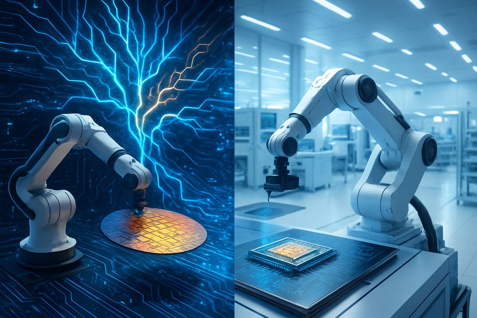
    The current wave of semiconductor innovation is characterized by a dramatic increase in transistor density and the adoption of novel transistor architectures. The 5nm node, in high-volume production since 2020, delivered a substantial boost in transistor count and performance over 7nm, becoming the bedrock for many current-generation AI accelerators. Building on this, the 3nm node, which entered high-volume production in 2022, offers a further 1.6x logic transistor density increase and 25-30% lower power consumption compared to 5nm. Notably, Samsung (KRX: 005930) introduced its 3nm Gate-All-Around (GAA) technology early, showcasing significant power efficiency gains.

    The most profound technical leap comes with the 2nm process node, where the industry is largely transitioning from the traditional FinFET architecture to Gate-All-Around (GAA) nanosheet transistors. GAAFETs provide superior electrostatic control over the transistor channel, dramatically reducing current leakage and improving drive current, which translates directly into enhanced performance and critical energy efficiency for AI workloads. TSMC (NYSE: TSM) is poised for mass production of its 2nm chips (N2) in the second half of 2025, while Intel (NASDAQ: INTC) is aggressively pursuing its Intel 18A (equivalent to 1.8nm) with its RibbonFET GAA architecture, aiming for leadership in 2025. These advancements also include the emergence of Backside Power Delivery Networks (BSPDN), further optimizing power efficiency. Initial reactions from the AI research community and industry experts highlight excitement over the potential for training even larger and more sophisticated LLMs, enabling more complex multi-modal AI, and pushing AI capabilities further into edge devices. The ability to pack more specialized AI accelerators and integrate next-generation High-Bandwidth Memory (HBM) like HBM4, offering roughly twice the bandwidth of HBM3, is seen as crucial for overcoming the "memory wall" that has bottlenecked AI hardware performance.

    Reshaping the AI Competitive Landscape

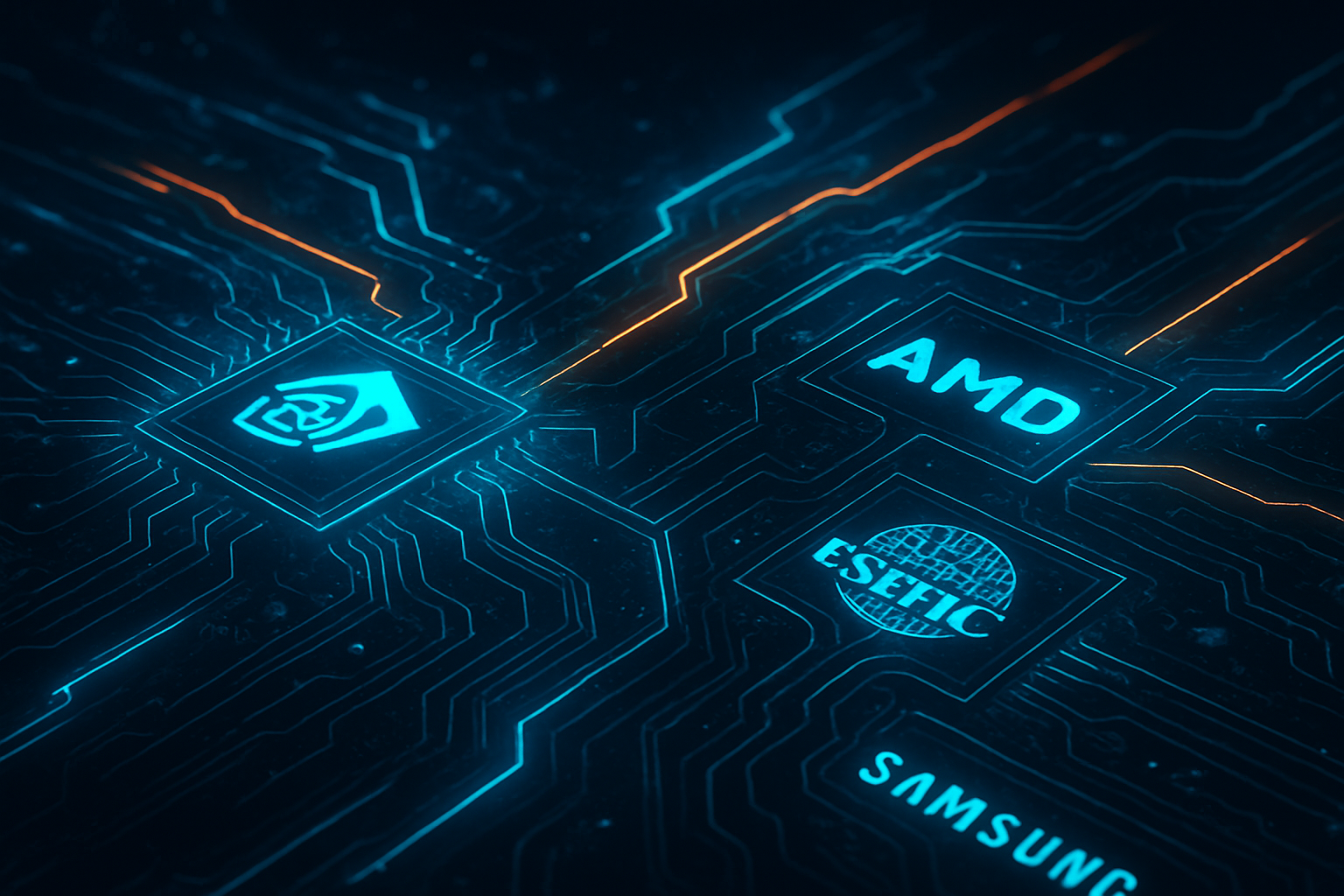
    These advanced semiconductor technologies are profoundly impacting the competitive dynamics among AI companies, tech giants, and startups. Foundries like TSMC (NYSE: TSM), which holds a commanding 92% market share in advanced AI chip manufacturing, and Samsung Foundry (KRX: 005930), are pivotal, providing the fundamental hardware for virtually all major AI players. Chip designers like NVIDIA (NASDAQ: NVDA) and AMD (NASDAQ: AMD) are direct beneficiaries, leveraging these smaller nodes and advanced packaging to create increasingly powerful GPUs and AI accelerators that dominate the market for AI training and inference. Intel, through its Intel Foundry Services (IFS), aims to regain process leadership with its 20A and 18A nodes, attracting significant interest from companies like Microsoft (NASDAQ: MSFT) for its custom AI chips.

    The competitive implications are immense. Companies that can secure access to these bleeding-edge fabrication processes will gain a significant strategic advantage, enabling them to offer superior performance-per-watt for AI workloads. This could disrupt existing product lines by making older hardware less competitive for demanding AI tasks. Tech giants such as Google (NASDAQ: GOOGL), Microsoft, and Meta Platforms (NASDAQ: META), which are heavily investing in custom AI silicon (like Google's TPUs), stand to benefit immensely, allowing them to optimize their AI infrastructure and reduce operational costs. Startups focused on specialized AI hardware or novel AI architectures will also find new avenues for innovation, provided they can navigate the high costs and complexities of advanced chip design. The "AI supercycle" is fueling unprecedented investment, intensifying competition among the leading foundries and memory manufacturers like SK Hynix (KRX: 000660) and Micron (NASDAQ: MU), particularly in the HBM space, as they vie to supply the critical components for the next generation of AI.

    Wider Implications for the AI Ecosystem

    The move beyond 7nm fits squarely into the broader AI landscape as a foundational enabler of the current and future AI boom. It addresses one of the most pressing challenges in AI: the insatiable demand for computational resources and energy. By providing more powerful and energy-efficient chips, these advancements allow for the training of larger, more complex AI models, including LLMs with trillions of parameters, which are at the heart of many recent AI breakthroughs. This directly impacts areas like natural language processing, computer vision, drug discovery, and autonomous systems.

    The impacts extend beyond raw performance. Enhanced power efficiency is crucial for mitigating the "energy crisis" faced by AI data centers, reducing operational costs, and making AI more sustainable. It also significantly boosts the capabilities of edge AI, enabling sophisticated AI processing on devices with limited power budgets, such as smartphones, IoT devices, and autonomous vehicles. This reduces reliance on cloud computing, improves latency, and enhances privacy. However, potential concerns exist. The astronomical cost of developing and manufacturing these advanced nodes, coupled with the immense capital expenditure required for foundries, could lead to a centralization of AI power among a few well-resourced tech giants and nations. The complexity of these processes also introduces challenges in yield and supply chain stability, as seen with ongoing geopolitical considerations driving efforts to strengthen domestic semiconductor manufacturing. These advancements are comparable to past AI milestones where hardware breakthroughs (like the advent of powerful GPUs for parallel processing) unlocked new eras of AI development, suggesting a similar transformative period ahead.

    The Road Ahead: Anticipating Future AI Horizons

    Looking ahead, the semiconductor roadmap extends even further into the nanoscale, promising continued advancements. TSMC (NYSE: TSM) has A16 (1.6nm-class) and A14 (1.4nm) on its roadmap, with A16 expected for production in late 2026 and A14 around 2028, leveraging next-generation High-NA EUV lithography. Samsung (KRX: 005930) plans mass production of its 1.4nm (SF1.4) chips by 2027, and Intel (NASDAQ: INTC) has Intel 14A slated for risk production in late 2026. These future nodes will further push the boundaries of transistor density and efficiency, enabling even more sophisticated AI models.

    Expected near-term developments include the widespread adoption of 2nm chips in flagship consumer electronics and enterprise AI accelerators, alongside the full commercialization of HBM4 memory, dramatically increasing memory bandwidth for AI. Long-term, we can anticipate the proliferation of heterogeneous integration and chiplet architectures, where specialized processing units and memory are seamlessly integrated within a single package, optimizing for specific AI workloads. Potential applications are vast, ranging from truly intelligent personal assistants and advanced robotics to hyper-personalized medicine and real-time climate modeling. Challenges that need to be addressed include the escalating costs of R&D and manufacturing, the increasing complexity of chip design (where AI itself is becoming a critical design tool), and the need for new materials and packaging innovations to continue scaling. Experts predict a future where AI hardware is not just faster, but also far more specialized and integrated, leading to an explosion of AI applications across every industry.

    A New Era of AI Defined by Silicon Prowess

    In summary, the rapid progression of semiconductor technology beyond 7nm, characterized by the widespread adoption of GAA transistors, advanced packaging techniques like 2.5D and 3D integration, and next-generation High-Bandwidth Memory (HBM4), marks a pivotal moment in the history of Artificial Intelligence. These innovations are creating the fundamental hardware bedrock for an unprecedented ascent of AI capabilities, enabling faster, more powerful, and significantly more energy-efficient AI systems. The ability to pack more transistors, reduce power consumption, and enhance data transfer speeds directly influences the capabilities and widespread deployment of machine learning and large language models.

    This development's significance in AI history cannot be overstated; it is as transformative as the advent of GPUs for deep learning. It's not just about making existing AI faster, but about enabling entirely new forms of AI that require immense computational resources. The long-term impact will be a pervasive integration of advanced AI into every facet of technology and society, from cloud data centers to edge devices. In the coming weeks and months, watch for announcements from major chip designers regarding new product lines leveraging 2nm technology, further details on HBM4 adoption, and strategic partnerships between foundries and AI companies. The race to the nanoscale continues, and with it, the acceleration of the AI revolution.


    This content is intended for informational purposes only and represents analysis of current AI developments.

    TokenRing AI delivers enterprise-grade solutions for multi-agent AI workflow orchestration, AI-powered development tools, and seamless remote collaboration platforms.
    For more information, visit https://www.tokenring.ai/.

  • Extreme Ultraviolet Lithography Market Set to Explode to $28.66 Billion by 2031, Fueling the Next Era of AI Chips

    Extreme Ultraviolet Lithography Market Set to Explode to $28.66 Billion by 2031, Fueling the Next Era of AI Chips

    The global Extreme Ultraviolet Lithography (EUL) market is on the cusp of unprecedented expansion, projected to reach a staggering $28.66 billion by 2031, exhibiting a robust Compound Annual Growth Rate (CAGR) of 22%. This explosive growth is not merely a financial milestone; it signifies a critical inflection point for the entire technology industry, particularly for advanced chip manufacturing. EUL is the foundational technology enabling the creation of the smaller, more powerful, and energy-efficient semiconductors that are indispensable for the next generation of artificial intelligence (AI), high-performance computing (HPC), 5G, and autonomous systems.

    This rapid market acceleration underscores the indispensable role of EUL in sustaining Moore's Law, pushing the boundaries of miniaturization, and providing the raw computational power required for the escalating demands of modern AI. As the world increasingly relies on sophisticated digital infrastructure and intelligent systems, the precision and capabilities offered by EUL are becoming non-negotiable, setting the stage for profound advancements across virtually every sector touched by computing.

    The Dawn of Sub-Nanometer Processing: How EUV is Redefining Chip Manufacturing

    Extreme Ultraviolet Lithography (EUL) represents a monumental leap in semiconductor fabrication, employing ultra-short wavelength light to etch incredibly intricate patterns onto silicon wafers. Unlike its predecessors, EUL utilizes light at a wavelength of approximately 13.5 nanometers (nm), a stark contrast to the 193 nm used in traditional Deep Ultraviolet (DUV) lithography. This significantly shorter wavelength is the key to EUL's superior resolution, enabling the production of features below 7 nm and paving the way for advanced process nodes such as 7nm, 5nm, 3nm, and even sub-2nm.

    The technical prowess of EUL systems is a marvel of modern engineering. The EUV light itself is generated by a laser-produced plasma (LPP) source, where high-power CO2 lasers fire at microscopic droplets of molten tin in a vacuum, creating an intensely hot plasma that emits EUV radiation. Because EUV light is absorbed by virtually all materials, the entire process must occur in a vacuum, and the optical system relies on a complex arrangement of highly specialized, ultra-smooth reflective mirrors. These mirrors, composed of alternating layers of molybdenum and silicon, are engineered to reflect 13.5 nm light with minimal loss. Photomasks, too, are reflective, differing from the transparent masks used in DUV, and are protected by thin, high-transmission pellicles. Current EUV systems (e.g., ASML's NXE series) operate with a 0.33 Numerical Aperture (NA), but the next generation, High-NA EUV, will increase this to 0.55 NA, promising even finer resolutions of 8 nm.

    This approach dramatically differs from previous methods, primarily DUV lithography. DUV systems use refractive lenses and operate in ambient air, relying heavily on complex and costly multi-patterning techniques (e.g., double or quadruple patterning) to achieve smaller feature sizes. These multi-step processes increase manufacturing complexity, defect rates, and overall costs. EUL, by contrast, enables single patterning for critical layers at advanced nodes, simplifying the manufacturing flow, reducing defectivity, and improving throughput. The initial reaction from the semiconductor industry has been one of immense investment and excitement, recognizing EUL as a "game-changer" and "essential" for sustaining Moore's Law. While the AI research community doesn't directly react to lithography as a field, they acknowledge EUL as a crucial enabling technology, providing the powerful chips necessary for their increasingly complex models. Intriguingly, AI and machine learning are now being integrated into EUV systems themselves, optimizing processes and enhancing efficiency.

    Corporate Titans and the EUV Arms Race: Shifting Power Dynamics in AI

    The proliferation of Extreme Ultraviolet Lithography is fundamentally reshaping the competitive landscape for AI companies, tech giants, and even startups, creating distinct advantages and potential disruptions. The ability to access and leverage EUL technology is becoming a strategic imperative, concentrating power among a select few industry leaders.

    Foremost among the beneficiaries is ASML Holding N.V. (NASDAQ: ASML), the undisputed monarch of the EUL market. As the world's sole producer of EUL machines, ASML's dominant position makes it indispensable for manufacturing cutting-edge chips. Its revenue is projected to grow significantly, fueled by AI-driven semiconductor demand and increasing EUL adoption. The rollout of High-NA EUL systems further solidifies ASML's long-term growth prospects, enabling breakthroughs in sub-2 nanometer transistor technologies. Following closely are the leading foundries and integrated device manufacturers (IDMs). Taiwan Semiconductor Manufacturing Company (NYSE: TSM), the largest pure-play foundry, heavily leverages EUL to produce advanced logic and memory chips for a vast array of tech companies. Their robust investments in global manufacturing capacity, driven by strong AI and HPC requirements, position them as a massive beneficiary. Similarly, Samsung Electronics Co., Ltd. (KRX: 005930) is a major producer and supplier that utilizes EUL to enhance its chip manufacturing capabilities, producing advanced processors and memory for its diverse product portfolio. Intel Corporation (NASDAQ: INTC) is also aggressively pursuing EUL, particularly High-NA EUL, to regain its leadership in chip manufacturing and produce 1.5nm and sub-1nm chips, crucial for its competitive positioning in the AI chip market.

    Chip designers like NVIDIA Corporation (NASDAQ: NVDA) and Advanced Micro Devices, Inc. (NASDAQ: AMD) are indirect but significant beneficiaries. While they don't manufacture EUL machines, their reliance on foundries like TSMC to produce their advanced AI GPUs and CPUs means that EUL-enabled fabrication directly translates to more powerful and efficient chips for their products. The demand for NVIDIA's AI accelerators, in particular, will continue to fuel the need for EUL-produced semiconductors. For tech giants operating vast cloud infrastructures and developing their own AI services, such as Alphabet Inc. (NASDAQ: GOOGL), Microsoft Corporation (NASDAQ: MSFT), and Amazon.com, Inc. (NASDAQ: AMZN), EUL-enabled chips power their data centers and AI offerings, allowing them to expand their market share as AI leaders. However, startups face considerable challenges due to the high operational costs and technical complexities of EUL, often needing to rely on tech giants for access to computing infrastructure. This dynamic could lead to increased consolidation and make it harder for smaller companies to compete on hardware innovation.

    The competitive implications are profound: EUL creates a significant divide. Companies with access to the most advanced EUL technology can produce superior chips, leading to increased performance for AI models, accelerated innovation cycles, and a centralization of resources among a few key players. This could disrupt existing products and services by making older hardware less competitive for demanding AI workloads and enabling entirely new categories of AI-powered devices. Strategically, EUL offers technology leadership, performance differentiation, long-term cost efficiency through higher yields, and enhanced supply chain resilience for those who master its complexities.

    Beyond the Wafer: EUV's Broad Impact on AI and the Global Tech Landscape

    Extreme Ultraviolet Lithography is not merely an incremental improvement in manufacturing; it is a foundational technology that underpins the current and future trajectory of Artificial Intelligence. By sustaining and extending Moore's Law, EUVL directly enables the exponential growth in computational capabilities that is the lifeblood of modern AI. Without EUVL, the relentless demand for more powerful, energy-efficient processors by large language models, deep neural networks, and autonomous systems would face insurmountable physical barriers, stifling innovation across the AI landscape.

    Its impact reverberates across numerous industries. In semiconductor manufacturing, EUVL is indispensable for producing the high-performance AI processors that drive global technological progress. Leading foundries and IDMs have fully integrated EUVL into their high-volume manufacturing lines for advanced process nodes, ensuring that companies at the forefront of AI development can produce more powerful, energy-efficient AI accelerators. For High-Performance Computing (HPC) and Data Centers, EUVL is critical for creating the advanced chips needed to power hyperscale data centers, which are the backbone of large language models and other data-intensive AI applications. Autonomous systems, such as self-driving cars and advanced robotics, directly benefit from the precision and power enabled by EUVL, allowing for faster and more efficient real-time decision-making. In consumer electronics, EUVL underpins the development of advanced AI features in smartphones, tablets, and IoT devices, enhancing user experiences. Even in medical and scientific research, EUVL-enabled chips facilitate breakthroughs in complex fields like drug discovery and climate modeling by providing unprecedented computational power.

    However, this transformative technology comes with significant concerns. The cost of EUL machines is extraordinary, with a single system costing hundreds of millions of dollars, and the latest High-NA models exceeding $370 million. Operational costs, including immense energy consumption (a single tool can rival the annual energy consumption of an entire city), further concentrate advanced chip manufacturing among a very few global players. The supply chain is also incredibly fragile, largely due to ASML's near-monopoly. Specialized components often come from single-source suppliers, making the entire ecosystem vulnerable to disruptions. Furthermore, EUL has become a potent factor in geopolitics, with export controls and technology restrictions, particularly those influenced by the United States on ASML's sales to China, highlighting EUVL as a "chokepoint" in global semiconductor manufacturing. This "techno-nationalism" can lead to market fragmentation and increased production costs.

    EUVL's significance in AI history can be likened to foundational breakthroughs such as the invention of the transistor or the development of the GPU. Just as these innovations enabled subsequent leaps in computing, EUVL provides the underlying hardware capability to manufacture the increasingly powerful processors required for AI. It has effectively extended the viability of Moore's Law, providing the hardware foundation necessary for the development of complex AI models. What makes this era unique is the emergent "AI supercycle," where AI and machine learning algorithms are also being integrated into EUVL systems themselves, optimizing fabrication processes and creating a powerful, self-improving technological feedback loop.

    The Road Ahead: Navigating the Future of Extreme Ultraviolet Lithography

    The future of Extreme Ultraviolet Lithography promises a relentless pursuit of miniaturization and efficiency, driven by the insatiable demands of AI and advanced computing. The coming years will witness several pivotal developments, pushing the boundaries of what's possible in chip manufacturing.

    In the near-term (present to 2028), the most significant advancement is the full introduction and deployment of High-NA EUV lithography. ASML (NASDAQ: ASML) has already shipped the first 0.55 NA scanner to Intel (NASDAQ: INTC), with high-volume manufacturing platforms expected to be operational by 2025. This leap in numerical aperture will enable even finer resolution patterns, crucial for sub-2nm nodes. Concurrently, there will be continued efforts to increase EUV light source power, enhancing wafer throughput, and to develop advanced photoresist materials and improved photomasks for higher precision and defect-free production. Looking further ahead (beyond 2028), research is already exploring Hyper-NA EUV with NAs of 0.75 or higher, and even shorter wavelengths, potentially below 5nm, to extend Moore's Law beyond 2030. Concepts like coherent light sources and Directed Self-Assembly (DSA) lithography are also on the horizon to further refine performance. Crucially, the integration of AI and machine learning into the entire EUV manufacturing process is expected to revolutionize optimization, predictive maintenance, and real-time adjustments.

    These advancements will unlock a new generation of applications and use cases. EUL will continue to drive the development of faster, more efficient, and powerful processors for Artificial Intelligence systems, including large language models and edge AI. It is essential for 5G and beyond telecommunications infrastructure, High-Performance Computing (HPC), and increasingly sophisticated autonomous systems. Furthermore, EUVL will play a vital role in advanced packaging technologies and 3D integration, allowing for greater levels of integration and miniaturization in chips. Despite the immense potential, significant challenges remain. High-NA EUV introduces complexities such as thinner photoresists leading to stochastic effects, reduced depth of focus, and enhanced mask 3D effects. Defectivity remains a persistent hurdle, requiring breakthroughs to achieve incredibly low defect rates for high-volume manufacturing. The cost of these machines and their immense operational energy consumption continue to be substantial barriers.

    Experts are unanimous in predicting substantial market growth for EUVL, reinforcing its role in extending Moore's Law and enabling chips at sub-2nm nodes. They foresee the continued dominance of foundries, driven by their focus on advanced-node manufacturing. Strategic investments from major players like TSMC (NYSE: TSM), Samsung (KRX: 005930), and Intel (NASDAQ: INTC), coupled with governmental support through initiatives like the U.S. CHIPS and Science Act, will accelerate EUV adoption. While EUV and High-NA EUV will drive advanced-node manufacturing, the industry will also need to watch for potential supply chain bottlenecks and the long-term viability of alternative lithography approaches being explored by various nations.

    EUV: A Cornerstone of the AI Revolution

    Extreme Ultraviolet Lithography stands as a testament to human ingenuity, a complex technological marvel that has become the indispensable backbone of the modern digital age. Its projected growth to $28.66 billion by 2031 with a 22% CAGR is not merely a market forecast; it is a clear indicator of its critical role in powering the ongoing AI revolution and shaping the future of technology. By enabling the production of smaller, more powerful, and energy-efficient chips, EUVL is directly responsible for the exponential leaps in computational capabilities that define today's advanced AI systems.

    The significance of EUL in AI history cannot be overstated. It has effectively "saved Moore's Law," providing the hardware foundation necessary for the development of complex AI models, from large language models to autonomous systems. Beyond its enabling role, EUVL systems are increasingly integrating AI themselves, creating a powerful feedback loop where advancements in AI drive the demand for sophisticated semiconductors, and these semiconductors, in turn, unlock new possibilities for AI. This symbiotic relationship ensures a continuous cycle of innovation, making EUVL a cornerstone of the AI era.

    Looking ahead, the long-term impact of EUVL will be profound and pervasive, driving sustained miniaturization, performance enhancement, and technological innovation across virtually every sector. It will facilitate the transition to even smaller process nodes, essential for next-generation consumer electronics, cloud computing, 5G, and emerging fields like quantum computing. However, the concentration of this critical technology in the hands of a single dominant supplier, ASML (NASDAQ: ASML), presents ongoing geopolitical and strategic challenges that will continue to shape global supply chains and international relations.

    In the coming weeks and months, industry observers should closely watch the full deployment and yield rates of High-NA EUV lithography systems by leading foundries, as these will be crucial indicators of their impact on future chip performance. Continued advancements in EUV components, particularly light sources and photoresist materials, will be vital for further enhancements. The increasing integration of AI and machine learning across the EUVL ecosystem, aimed at optimizing efficiency and precision, will also be a key trend. Finally, geopolitical developments, export controls, and government incentives will continue to influence regional fab expansions and the global competitive landscape, all of which will determine the pace and direction of the AI revolution powered by Extreme Ultraviolet Lithography.


    This content is intended for informational purposes only and represents analysis of current AI developments.

    TokenRing AI delivers enterprise-grade solutions for multi-agent AI workflow orchestration, AI-powered development tools, and seamless remote collaboration platforms.
    For more information, visit https://www.tokenring.ai/.

  • The Great Chip Divide: AI Supercycle Fuels Foundry Boom While Traditional Sectors Navigate Recovery

    The Great Chip Divide: AI Supercycle Fuels Foundry Boom While Traditional Sectors Navigate Recovery

    The global semiconductor industry, a foundational pillar of modern technology, is currently experiencing a profound and unprecedented bifurcation as of October 2025. While an "AI Supercycle" is driving insatiable demand for cutting-edge chips, propelling industry leaders to record profits, traditional market segments like consumer electronics, automotive, and industrial computing are navigating a more subdued recovery from lingering inventory corrections. This dual reality presents both immense opportunities and significant challenges for the world's top chip foundries – Taiwan Semiconductor Manufacturing Company (TSMC) (NYSE: TSM), Intel (NASDAQ: INTC), and Samsung (KRX: 005930) – reshaping the competitive landscape and dictating the future of technological innovation.

    This dynamic environment highlights a stark contrast: the relentless pursuit of advanced silicon for artificial intelligence applications is pushing manufacturing capabilities to their limits, while other sectors cautiously emerge from a period of oversupply. The immediate significance lies in the strategic reorientation of these foundry giants, who are pouring billions into expanding advanced node capacity, diversifying global footprints, and aggressively competing for the lucrative AI chip contracts that are now the primary engine of industry growth.

    Navigating a Bifurcated Market: The Technical Underpinnings of Current Demand

    The current semiconductor market is defined by a "tale of two markets." On one side, the demand for specialized, cutting-edge AI chips, particularly advanced GPUs, high-bandwidth memory (HBM), and sub-11nm geometries (e.g., 7nm, 5nm, 3nm, and emerging 2nm), is overwhelming. Sales of generative AI chips alone are forecasted to surpass $150 billion in 2025, with AI accelerators projected to exceed this figure. This demand is concentrated on a few advanced foundries capable of producing these complex components, leading to unprecedented utilization rates for leading-edge nodes and advanced packaging solutions like CoWoS (Chip-on-Wafer-on-Substrate).

    Conversely, traditional market segments, while showing signs of gradual recovery, still face headwinds. Consumer electronics, including smartphones and PCs, are experiencing muted demand and slower recovery for mature node semiconductors, despite the anticipated doubling of sales for AI-enabled PCs and mobile devices in 2025. The automotive and industrial sectors, which underwent significant inventory corrections in early 2025, are seeing demand improve in the second half of the year as restocking efforts pick up. However, a looming shortage of mature node chips (40nm and above) is still anticipated for the automotive industry in late 2025 or 2026, despite some easing of previous shortages.

    This situation differs significantly from previous semiconductor downturns or upswings, which were often driven by broad-based demand for PCs or smartphones. The defining characteristic of the current upswing is the insatiable demand for AI chips, which requires vastly more sophisticated, power-efficient designs. This pushes the boundaries of advanced manufacturing and creates a bifurcated market where advanced node utilization remains strong, while mature node foundries face a slower, more cautious recovery. Macroeconomic factors, including geopolitical tensions and trade policies, continue to influence the supply chain, with initiatives like the U.S. CHIPS Act aiming to bolster domestic manufacturing but also contributing to a complex global competitive landscape.

    Initial reactions from the industry underscore this divide. TSMC reported record results in Q3 2025, with profit jumping 39% year-on-year and revenue rising 30.3% to $33.1 billion, largely due to AI demand described as "stronger than we thought three months ago." Intel's foundry business, while still operating at a loss, is seen as having a significant opportunity due to the AI boom, with Microsoft reportedly committing to use Intel Foundry for its next in-house AI chip. Samsung Foundry, despite a Q1 2025 revenue decline, is aggressively expanding its presence in the HBM market and advancing its 2nm process, aiming to capture a larger share of the AI chip market.

    The AI Supercycle's Ripple Effect: Impact on Tech Giants and Startups

    The bifurcated chip market is having a profound and varied impact across the technology ecosystem, from established tech giants to nimble AI startups. Companies deeply entrenched in the AI and data center space are reaping unprecedented benefits, while others must strategically adapt to avoid being left behind.

    NVIDIA (NASDAQ: NVDA) remains a dominant force, reportedly nearly doubling its brand value in 2025, driven by the explosive demand for its GPUs and the robust CUDA software ecosystem. NVIDIA has reportedly booked nearly all capacity at partner server plants through 2026 for its Blackwell and Rubin platforms, indicating hardware bottlenecks and potential constraints for other firms. AMD (NASDAQ: AMD) is making significant inroads in the AI and data center chip markets with its AI accelerators and CPU/GPU offerings, with Microsoft reportedly co-developing chips with AMD, intensifying competition.

    Hyperscalers like Google (NASDAQ: GOOGL), Microsoft (NASDAQ: MSFT), and Amazon (NASDAQ: AMZN) are heavily investing in their own custom AI chips (ASICs), such as Google's TPUs, Amazon's Graviton and Trainium, and Microsoft's rumored in-house AI chip. This strategy aims to reduce dependency on third-party suppliers, optimize performance for their specific software needs, and control long-term costs. While developing their own silicon, these tech giants still heavily rely on NVIDIA's GPUs for their cloud computing businesses, creating a complex supplier-competitor dynamic. For startups, the astronomical cost of developing and manufacturing advanced AI chips creates a massive barrier, potentially centralizing AI power among a few tech giants. However, increased domestic manufacturing and specialized niches offer new opportunities.

    For the foundries themselves, the stakes are exceptionally high. TSMC (NYSE: TSM) remains the undisputed leader in advanced nodes and advanced packaging, critical for AI accelerators. Its market share in Foundry 1.0 is projected to climb to 66% in 2025, and it is accelerating capacity expansion with significant capital expenditure. Samsung Foundry (KRX: 005930) is aggressively positioning itself as a "one-stop shop" by leveraging its expertise across memory, foundry, and advanced packaging, aiming to reduce manufacturing times and capture a larger market share, especially with its early adoption of Gate-All-Around (GAA) transistor architecture. Intel (NASDAQ: INTC) is making a strategic pivot with Intel Foundry Services (IFS) to become a major AI chip manufacturer. The explosion in AI accelerator demand and limited advanced manufacturing capacity at TSMC create a significant opportunity for Intel, bolstered by strong support from the U.S. government through the CHIPS Act. However, Intel faces the challenge of overcoming a history of manufacturing delays and building customer trust in its foundry business.

    A New Era of Geopolitics and Technological Sovereignty: Wider Significance

    The demand challenges in the chip foundry industry, particularly the AI-driven market bifurcation, signify a fundamental reshaping of the broader AI landscape and global technological order. This era is characterized by an unprecedented convergence of technological advancement, economic competition, and national security imperatives.

    The "AI Supercycle" is driving not just innovation in chip design but also in how AI itself is leveraged to accelerate chip development, potentially leading to fully autonomous fabrication plants. However, this intense focus on AI could lead to a diversion of R&D and capital from non-AI sectors, potentially slowing innovation in areas less directly tied to cutting-edge AI. A significant concern is the concentration of power. TSMC's dominance (over 70% in global pure-play wafer foundry and 92% in advanced AI chip manufacturing) creates a highly concentrated AI hardware ecosystem, establishing high barriers to entry and significant dependencies. Similarly, the gains from the AI boom are largely concentrated among a handful of key suppliers and distributors, raising concerns about market monopolization.

    Geopolitical risks are paramount. The ongoing U.S.-China trade war, including export controls on advanced semiconductors and manufacturing equipment, is fragmenting the global supply chain into regional ecosystems, leading to a "Silicon Curtain." The proposed GAIN AI Act in the U.S. Senate in October 2025, requiring domestic chipmakers to prioritize U.S. buyers before exporting advanced semiconductors to "national security risk" nations, further highlights these tensions. The concentration of advanced manufacturing in East Asia, particularly Taiwan, creates significant strategic vulnerabilities, with any disruption to TSMC's production having catastrophic global consequences.

    This period can be compared to previous semiconductor milestones where hardware re-emerged as a critical differentiator, echoing the rise of specialized GPUs or the distributed computing revolution. However, unlike earlier broad-based booms, the current AI-driven surge is creating a more nuanced market. For national security, advanced AI chips are strategic assets, vital for military applications, 5G, and quantum computing. Economically, the "AI supercycle" is a foundational shift, driving aggressive national investments in domestic manufacturing and R&D to secure leadership in semiconductor technology and AI, despite persistent talent shortages.

    The Road Ahead: Future Developments and Expert Predictions

    The next few years will be pivotal for the chip foundry industry, as it navigates sustained AI growth, traditional market recovery, and complex geopolitical dynamics. Both near-term (6-12 months) and long-term (1-5 years) developments will shape the competitive landscape and unlock new technological frontiers.

    In the near term (October 2025 – September 2026), TSMC (NYSE: TSM) is expected to begin high-volume manufacturing of its 2nm chips in Q4 2025, with major customers driving demand. Its CoWoS advanced packaging capacity is aggressively scaling, aiming to double output in 2025. Intel Foundry (NASDAQ: INTC) is in a critical period for its "five nodes in four years" plan, targeting leadership with its Intel 18A node, incorporating RibbonFET and PowerVia technologies. Samsung Foundry (KRX: 005930) is also focused on advancing its 2nm Gate-All-Around (GAA) process for mass production in 2025, targeting mobile, HPC, AI, and automotive applications, while bolstering its advanced packaging capabilities.

    Looking long-term (October 2025 – October 2030), AI and HPC will continue to be the primary growth engines, requiring 10x more compute power by 2030 and accelerating the adoption of sub-2nm nodes. The global semiconductor market is projected to surpass $1 trillion by 2030. Traditional segments are also expected to recover, with automotive undergoing a profound transformation towards electrification and autonomous driving, driving demand for power semiconductors and automotive HPC. Foundries like TSMC will continue global diversification, Intel aims to become the world's second-largest foundry by 2030, and Samsung plans for 1.4nm chips by 2027, integrating advanced packaging and memory.

    Potential applications on the horizon include "AI Everywhere," with optimized products featuring on-device AI in smartphones and PCs, and generative AI driving significant cloud computing demand. Autonomous driving, 5G/6G networks, advanced healthcare devices, and industrial automation will also be major drivers. Emerging computing paradigms like neuromorphic and quantum computing are also projected for commercial take-off.

    However, significant challenges persist. A global, escalating talent shortage threatens innovation, requiring over one million additional skilled workers globally by 2030. Geopolitical stability remains precarious, with efforts to diversify production and reduce dependencies through government initiatives like the U.S. CHIPS Act facing high manufacturing costs and potential market distortion. Sustainability concerns, including immense energy consumption and water usage, demand more energy-efficient designs and processes. Experts predict a continued "AI infrastructure arms race," deeper integration between AI developers and hardware manufacturers, and a shifting competitive landscape where TSMC maintains leadership in advanced nodes, while Intel and Samsung aggressively challenge its dominance.

    A Transformative Era: The AI Supercycle's Enduring Legacy

    The current demand challenges facing the world's top chip foundries underscore an industry in the midst of a profound transformation. The "AI Supercycle" has not merely created a temporary boom; it has fundamentally reshaped market dynamics, technological priorities, and geopolitical strategies. The bifurcated market, with its surging AI demand and recovering traditional segments, reflects a new normal where specialized, high-performance computing is paramount.

    The strategic maneuvers of TSMC (NYSE: TSM), Intel (NASDAQ: INTC), and Samsung (KRX: 005930) are critical. TSMC's continued dominance in advanced nodes and packaging, Samsung's aggressive push into 2nm GAA and integrated solutions, and Intel's ambitious IDM 2.0 strategy to reclaim foundry leadership, all point to an intense, multi-front competition that will drive unprecedented innovation. This era signifies a foundational shift in AI history, where AI is not just a consumer of chips but an active participant in their design and optimization, fostering a symbiotic relationship that pushes the boundaries of computational power.

    The long-term impact on the tech industry and society will be characterized by ubiquitous, specialized, and increasingly energy-efficient computing, unlocking new applications that were once the realm of science fiction. However, this future will unfold within a fragmented global semiconductor market, where technological sovereignty and supply chain resilience are national security imperatives. The escalating "talent war" and the immense capital expenditure required for advanced fabs will further concentrate power among a few key players.

    What to watch for in the coming weeks and months:

    • Intel's 18A Process Node: Its progress and customer adoption will be a key indicator of its foundry ambitions.
    • 2nm Technology Race: The mass production timelines and yield rates from TSMC and Samsung will dictate their competitive standing.
    • Geopolitical Stability: Any shifts in U.S.-China trade tensions or cross-strait relations will have immediate repercussions.
    • Advanced Packaging Capacity: TSMC's ability to meet the surging demand for CoWoS and other advanced packaging will be crucial for the AI hardware ecosystem.
    • Talent Development Initiatives: Progress in addressing the industry's talent gap is essential for sustaining innovation.
    • Market Divergence: Continue to monitor the performance divergence between companies heavily invested in AI and those serving more traditional markets. The resilience and adaptability of companies in less AI-centric sectors will be key.
    • Emergence of Edge AI and NPUs: Observe the pace of adoption and technological advancements in edge AI and specialized NPUs, signaling a crucial shift in how AI processing is distributed and consumed.

    The semiconductor industry is not merely witnessing growth; it is undergoing a fundamental transformation, driven by an "AI supercycle" and reshaped by geopolitical forces. The coming months will be pivotal in determining the long-term leaders and the eventual structure of this indispensable global industry.


    This content is intended for informational purposes only and represents analysis of current AI developments.

    TokenRing AI delivers enterprise-grade solutions for multi-agent AI workflow orchestration, AI-powered development tools, and seamless remote collaboration platforms.
    For more information, visit https://www.tokenring.ai/.

  • Samsung Ignites India’s AI Ambition with Strategic Chip and Memory R&D Surge

    Samsung Ignites India’s AI Ambition with Strategic Chip and Memory R&D Surge

    Samsung's strategic expansion in India is underpinned by a robust technical agenda, focusing on cutting-edge advancements in chip design and memory solutions crucial for the AI era. Samsung Semiconductor India Research (SSIR) is now a tripartite powerhouse, encompassing R&D across memory, System LSI (custom chips/System-on-Chip or SoC), and foundry technologies. This comprehensive approach allows Samsung to develop integrated hardware solutions, optimizing performance and efficiency for diverse AI workloads.

    The company's aggressive hiring drive in India targets highly specialized roles, including System-on-Chip (SoC) design engineers, memory design engineers (with a strong emphasis on High Bandwidth Memory, or HBM, for AI servers), SSD firmware developers, and graphics driver engineers. These roles are specifically geared towards advancing next-generation technologies such as AI computation optimization, seamless system semiconductor integration, and sophisticated advanced memory design. This focus on specialized talent underscores Samsung's commitment to pushing the boundaries of AI hardware.

    Technically, Samsung is at the forefront of advanced process nodes. The company anticipates mass-producing its second-generation 3-nanometer chips using Gate-All-Around (GAA) technology in the latter half of 2024, a significant leap in semiconductor manufacturing. Looking further ahead, Samsung aims to implement its 2-nanometer chipmaking process for high-performance computing chips by 2027. Furthermore, in June 2024, Samsung unveiled a "one-stop shop" solution for clients, integrating its memory chip, foundry, and chip packaging services. This streamlined process is designed to accelerate AI chip production by approximately 20%, offering a compelling value proposition to AI developers seeking faster time-to-market for their hardware. The emphasis on HBM, particularly HBM3E, is critical, as these high-performance memory chips are indispensable for feeding the massive data requirements of large language models and other complex AI applications.

    Initial reactions from the AI research community and industry experts highlight the strategic brilliance of Samsung's move. Leveraging India's vast pool of over 150,000 skilled chip design engineers, Samsung is transforming India's image from a cost-effective delivery center to a "capability-led" strategic design hub. This not only bolsters Samsung's global R&D capabilities but also aligns perfectly with India's "Semicon India" initiative, aiming to cultivate a robust domestic semiconductor ecosystem. The synergy between Samsung's global ambition and India's national strategic goals is expected to yield significant technological breakthroughs and foster a vibrant local innovation landscape.

    Reshaping the AI Hardware Battleground: Competitive Implications

    Samsung's expanded AI chip and memory R&D in India is poised to intensify competition across the entire AI semiconductor value chain, affecting market leaders and challengers alike. As a vertically integrated giant with strengths in memory manufacturing, foundry services, and chip design (System LSI), Samsung (KRX: 005930) is uniquely positioned to offer optimized "full-stack" solutions for AI chips, potentially leading to greater efficiency and customizability.

    For NVIDIA (NASDAQ: NVDA), the current undisputed leader in AI GPUs, Samsung's enhanced AI chip design capabilities, particularly in custom silicon and specialized AI accelerators, could introduce more direct competition. While NVIDIA's CUDA ecosystem remains a formidable moat, Samsung's full-stack approach might enable it to offer highly optimized and potentially more cost-effective solutions for specific AI inference workloads or on-device AI applications, challenging NVIDIA's dominance in certain segments.

    Intel (NASDAQ: INTC), actively striving to regain market share in AI, will face heightened rivalry from Samsung's strengthened R&D. Samsung's ability to develop advanced AI accelerators and its foundry capabilities directly compete with Intel's efforts in both chip design and manufacturing services. The race for top engineering talent, particularly in SoC design and AI computation optimization, is also expected to escalate between the two giants.

    In the foundry space, TSMC (NYSE: TSM), the world's largest dedicated chip foundry, will encounter increased competition from Samsung's expanding foundry R&D in India. Samsung's aggressive push to enhance its process technology (e.g., 3nm GAA, 2nm by 2027) and packaging solutions aims to offer a strong alternative to TSMC for advanced AI chip fabrication, as evidenced by its existing contracts to mass-produce AI chips for companies like Tesla.

    For memory powerhouses like SK Hynix (KRX: 000660) and Micron (NASDAQ: MU), both dominant players in High Bandwidth Memory (HBM), Samsung's substantial expansion in memory R&D in India, including HBM, directly intensifies competition. Samsung's efforts to develop advanced HBM and seamlessly integrate it with its AI chip designs and foundry services could challenge their market leadership and impact HBM pricing and market share dynamics.

    AMD (NASDAQ: AMD), a formidable challenger in the AI chip market with its Instinct MI300X series, could also face increased competition. If Samsung develops competitive AI GPUs or specialized AI accelerators, it could directly vie for contracts with major AI labs and cloud providers. Interestingly, Samsung is also a primary supplier of HBM4 for AMD's MI450 accelerator, illustrating a complex dynamic of both competition and interdependence. Major AI labs and tech companies are increasingly seeking custom AI silicon, and Samsung's comprehensive capabilities make it an attractive "full-stack" partner, offering integrated, tailor-made solutions that could provide cost efficiencies or performance advantages, ultimately benefiting the broader AI ecosystem through diversified supply options.

    Broader Strokes: Samsung's Impact on the Global AI Canvas

    Samsung's expanded AI chip and memory R&D in India is not merely a corporate strategy; it's a significant inflection point with profound implications for the global AI landscape, semiconductor supply chain, and India's rapidly ascending tech sector. This move aligns with a broader industry trend towards "AI Phones" and pervasive on-device AI, where AI becomes the primary user interface, integrating seamlessly with applications and services. Samsung's focus on developing localized AI features, particularly for Indian languages, underscores a commitment to personalization and catering to diverse global user bases, recognizing India's high AI adoption rate.

    The initiative directly addresses the escalating demand for advanced semiconductor hardware driven by increasingly complex and larger AI models. By focusing on next-generation technologies like SoC design, HBM, and advanced memory, Samsung (KRX: 005930) is actively shaping the future of AI processing, particularly for edge computing and ambient intelligence applications where AI workloads shift from centralized data centers to devices. This decentralization of AI processing demands high-performance, low-latency, and power-efficient semiconductors, areas where Samsung's R&D in India is expected to make significant contributions.

    For the global semiconductor supply chain, Samsung's investment signifies a crucial step towards diversification and resilience. By transforming SSIR into a core global design stronghold for AI semiconductors, Samsung is reducing over-reliance on a few geographical hubs, a critical move in light of recent geopolitical tensions and supply chain vulnerabilities. This elevates India's role in the global semiconductor value chain, attracting further foreign direct investment and fostering a more robust, distributed ecosystem. This aligns perfectly with India's "Semicon India" initiative, which aims to establish a domestic semiconductor manufacturing and design ecosystem, projecting the Indian chip market to reach an impressive $100 billion by 2030.

    While largely positive, potential concerns include intensified talent competition for skilled AI and semiconductor engineers in India, potentially exacerbating existing skills gaps. Additionally, the global semiconductor industry remains susceptible to geopolitical factors, such as trade restrictions on AI chip sales, which could introduce uncertainties despite Samsung's diversification efforts. However, this expansion can be compared to previous AI milestones, such as the internet revolution and the transition from feature phones to smartphones. Samsung executives describe the current shift as the "next big revolution," with AI poised to transform all aspects of technology, making it a commercialized product accessible to a mass market, much like previous technological paradigm shifts.

    The Road Ahead: Anticipating Future AI Horizons

    Samsung's expanded AI chip and memory R&D in India sets the stage for a wave of transformative developments in the near and long term. In the immediate future (1-3 years), consumers can expect significant enhancements across Samsung's product portfolio. Flagship devices like the upcoming Galaxy S25 Ultra, Galaxy Z Fold7, and Galaxy Z Flip7 are poised to integrate advanced AI tools such as Live Translate, Note Assist, Circle to Search, AI wallpaper, and an audio eraser, providing seamless and intuitive user experiences. A key focus will be on India-centric AI localization, with features supporting nine Indian languages in Galaxy AI and tailored functionalities for home appliances designed for local conditions, such as "Stain Wash" and "Customised Cooling." Samsung (KRX: 005930) aims for AI-powered products to constitute 70% of its appliance sales by the end of 2025, further expanding the SmartThings ecosystem for automated routines, energy efficiency, and personalized experiences.

    Looking further ahead (3-10+ years), Samsung predicts a fundamental shift from traditional smartphones to "AI phones" that leverage a hybrid approach of on-device and cloud-based AI models, with India playing a critical role in the development of cutting-edge chips, including advanced process nodes like 2-nanometer technology. Pervasive AI integration will extend beyond current devices, foundational for future advancements like 6G communication and deeply embedding AI across Samsung's entire product portfolio, from wellness and healthcare to smart urban environments. Expert predictions widely anticipate India solidifying its position as a key hub for semiconductor design in the AI era, with the Indian semiconductor market projected to reach USD 100 billion by 2030, strongly supported by government initiatives like the "Semicon India" program.

    However, several challenges need to be addressed. The development of advanced AI chips demands significant capital investment and a highly specialized workforce, despite India's large talent pool. India's current lack of large-scale semiconductor fabrication units necessitates reliance on foreign foundries, creating a dependency on imported chips and AI hardware. Geopolitical factors, such as export restrictions on AI chips, could also hinder India's AI development by limiting access to crucial GPUs. Addressing these challenges will require continuous investment in education, infrastructure, and strategic international partnerships to ensure India can fully capitalize on its growing AI and semiconductor prowess.

    A New Chapter in AI: Concluding Thoughts

    Samsung's (KRX: 005930) strategic expansion of its AI chip and memory R&D in India marks a pivotal moment in the global artificial intelligence landscape. This comprehensive initiative, transforming Samsung Semiconductor India Research (SSIR) into a core global design stronghold, underscores Samsung's long-term commitment to leading the AI revolution. The key takeaways are clear: Samsung is leveraging India's vast engineering talent to accelerate the development of next-generation AI hardware, from advanced process nodes like 3nm GAA and future 2nm chips to high-bandwidth memory (HBM) solutions. This move not only bolsters Samsung's competitive edge against rivals like NVIDIA (NASDAQ: NVDA), Intel (NASDAQ: INTC), TSMC (NYSE: TSM), SK Hynix (KRX: 000660), Micron (NASDAQ: MU), and AMD (NASDAQ: AMD) but also significantly elevates India's standing as a global hub for high-value semiconductor design and innovation.

    The significance of this development in AI history cannot be overstated. It represents a strategic decentralization of advanced R&D, contributing to a more resilient global semiconductor supply chain and fostering a vibrant domestic tech ecosystem in India. The long-term impact will be felt across consumer electronics, smart home technologies, healthcare, and beyond, as AI becomes increasingly pervasive and personalized. Samsung's vision of "AI Phones" and a hybrid AI approach, coupled with a focus on localized AI solutions, promises to reshape user interaction with technology fundamentally.

    In the coming weeks and months, industry watchers should keenly observe Samsung's recruitment progress in India, specific technical breakthroughs emerging from SSIR, and further partnerships or supply agreements for its advanced AI chips and memory. The interplay between Samsung's aggressive R&D and India's "Semicon India" initiative will be crucial in determining the pace and scale of India's emergence as a global AI and semiconductor powerhouse. This strategic investment is not just about building better chips; it's about building the future of AI, with India at its heart.


    This content is intended for informational purposes only and represents analysis of current AI developments.

    TokenRing AI delivers enterprise-grade solutions for multi-agent AI workflow orchestration, AI-powered development tools, and seamless remote collaboration platforms.
    For more information, visit https://www.tokenring.ai/.

  • The Silicon Frontier: How Advanced Manufacturing is Powering AI’s Unprecedented Ascent

    The Silicon Frontier: How Advanced Manufacturing is Powering AI’s Unprecedented Ascent

    The world of artificial intelligence is undergoing a profound transformation, fueled by an insatiable demand for processing power that pushes the very limits of semiconductor technology. As of late 2025, the advanced chip manufacturing sector is in a state of unprecedented growth and rapid innovation, with leading foundries like Taiwan Semiconductor Manufacturing Company (TSMC) (NYSE: TSM) spearheading massive expansion efforts to meet the escalating needs of AI. This surge in demand, particularly for high-performance semiconductors, is not merely driving the industry; it is fundamentally reshaping it, creating a symbiotic relationship where AI both consumes and enables the next generation of chip fabrication.

    The immediate significance of these developments lies in AI's exponential growth across diverse fields—from generative AI and edge computing to autonomous systems and high-performance computing (HPC). These applications necessitate processors that are not only faster and smaller but also significantly more energy-efficient, placing immense pressure on the semiconductor ecosystem. The global semiconductor market is projected to see substantial growth in 2025, with the AI chip market alone expected to exceed $150 billion, underscoring the critical role of advanced manufacturing in powering the AI revolution.

    Engineering the Future: The Technical Marvels Behind AI's Brains

    At the forefront of current manufacturing capabilities are leading-edge nodes such as 3nm and the rapidly emerging 2nm. TSMC, the dominant foundry, is poised for mass production of its 2nm chips in the second half of 2025, with even more advanced process nodes like A16 (1.6nm-class) and A14 (1.4nm) already on the roadmap for future production, expected in late 2026 and around 2028, respectively. This relentless pursuit of smaller, more powerful transistors is defining the future of AI hardware.

    Beyond traditional silicon scaling, advanced packaging technologies have become critical. As Moore's Law encounters physical and economic barriers, innovations like 2.5D and 3D integration, chiplets, and fan-out packaging enable heterogeneous integration—combining multiple components like processors, memory, and specialized accelerators within a single package. TSMC's Chip-on-Wafer-on-Substrate (CoWoS) is a leading 2.5D technology, with its capacity projected to quadruple by the end of 2025. Similarly, its SoIC (System-on-Integrated-Chips) 3D stacking technology is slated for mass production this year. Hybrid bonding, which uses direct copper-to-copper bonds, and emerging glass substrates further enhance these packaging solutions, offering significant improvements in performance, power, and cost for AI applications.

    Another pivotal innovation is the transition from FinFET (Fin Field-Effect Transistor) to Gate-All-Around FET (GAAFET) technology at sub-5-nanometer nodes. GAAFETs, which encapsulate the transistor channel on all sides, offer enhanced gate control, reduced power consumption, improved speed, and higher transistor density, overcoming the limitations of FinFETs. TSMC is introducing its nanosheet transistor architecture at the 2nm node by 2025, while Samsung (KRX: 005930) is refining its MBCFET-based 3nm process, and Intel (NASDAQ: INTC) plans to adopt RibbonFET for its 18A node, marking a global race in GAAFET adoption. These advancements represent a significant departure from previous transistor designs, allowing for the creation of far more complex and efficient AI chips.

    Extreme Ultraviolet (EUV) lithography remains indispensable for producing these advanced nodes. Recent advancements include the integration of AI and ML algorithms into EUV systems to optimize fabrication processes, from predictive maintenance to real-time adjustments. Intriguingly, geopolitical factors are also spurring developments in this area, with China reportedly testing a domestically developed EUV system for trial production in Q3 2025, targeting mass production by 2026, and Russia outlining its own EUV roadmap from 2026. This highlights a global push for technological self-sufficiency in critical manufacturing tools. Furthermore, AI is not just a consumer of advanced chips but also a powerful enabler in their creation. AI-powered Electronic Design Automation (EDA) tools, such as Synopsys (NASDAQ: SNPS) DSO.ai, leverage machine learning to automate repetitive tasks, optimize power, performance, and area (PPA), and dramatically reduce chip design timelines. In manufacturing, AI is deployed for predictive maintenance, real-time process optimization, and highly accurate defect detection, leading to increased production efficiency, reduced waste, and improved yields. AI also enhances supply chain management by optimizing logistics and predicting material shortages, creating a more resilient and cost-effective network.

    Reshaping the AI Landscape: Corporate Impacts and Competitive Edges

    The rapid evolution in advanced chip manufacturing is profoundly impacting AI companies, tech giants, and startups, creating both immense opportunities and fierce competitive pressures. Companies at the forefront of AI development, particularly those designing high-performance AI accelerators, stand to benefit immensely. NVIDIA (NASDAQ: NVDA), a leader in AI semiconductor technology, is a prime example, reporting a staggering 200% year-over-year increase in data center GPU sales, reflecting the insatiable demand for its cutting-edge AI chips that heavily rely on TSMC's advanced nodes and packaging.

    The competitive implications for major AI labs and tech companies are significant. Access to leading-edge process nodes and advanced packaging becomes a crucial differentiator. Companies like Google (NASDAQ: GOOGL), Microsoft (NASDAQ: MSFT), and Amazon (NASDAQ: AMZN), all heavily invested in AI infrastructure and custom AI silicon (e.g., Google's TPUs, AWS's Inferentia/Trainium), are directly reliant on the capabilities of foundries like TSMC and their ability to deliver increasingly powerful and efficient chips. Those with strategic foundry partnerships and early access to the latest technologies will gain a substantial advantage in deploying more powerful AI models and services.

    This development also has the potential to disrupt existing products and services. AI-powered capabilities, once confined to cloud data centers, are increasingly migrating to the edge and consumer devices, thanks to more efficient and powerful chips. This could lead to a major PC refresh cycle as generative AI transforms consumer electronics, demanding AI-integrated applications and hardware. Companies that can effectively integrate these advanced chips into their product lines—from smartphones to autonomous vehicles—will gain significant market positioning and strategic advantages. The demand for next-generation GPUs, for instance, is reportedly outstripping supply by a 10:1 ratio, highlighting the scarcity and strategic importance of these components. Furthermore, the memory segment is experiencing a surge, with high-bandwidth memory (HBM) products like HBM3 and HBM3e, essential for AI accelerators, driving over 24% growth in 2025, with HBM4 expected in H2 2025. This interconnected demand across the hardware stack underscores the strategic importance of the entire advanced manufacturing ecosystem.

    A New Era for AI: Broader Implications and Future Horizons

    The advancements in chip manufacturing fit squarely into the broader AI landscape as the fundamental enabler of increasingly complex and capable AI models. Without these breakthroughs in silicon, the computational demands of large language models, advanced computer vision, and sophisticated reinforcement learning would be insurmountable. This era marks a unique inflection point where hardware innovation directly dictates the pace and scale of AI progress, moving beyond software-centric breakthroughs to a symbiotic relationship where both must advance in tandem.

    The impacts are wide-ranging. Economically, the semiconductor industry is experiencing a boom, attracting massive capital expenditures. TSMC alone plans to construct nine new facilities in 2025—eight new fabrication plants and one advanced packaging plant—with a capital expenditure projected between $38 billion and $42 billion. Geopolitically, the race for advanced chip manufacturing dominance is intensifying. U.S. export restrictions, tariff pressures, and efforts by nations like China and Russia to achieve self-sufficiency in critical technologies like EUV lithography are reshaping global supply chains and manufacturing strategies. Concerns around supply chain resilience, talent shortages, and the environmental impact of energy-intensive manufacturing processes are also growing.

    Compared to previous AI milestones, such as the advent of deep learning or the transformer architecture, these hardware advancements are foundational. They are not merely enabling incremental improvements but are providing the raw horsepower necessary for entirely new classes of AI applications and models that were previously impossible. The sheer power demands of AI workloads also emphasize the critical need for innovations that improve energy efficiency, such as GAAFETs and novel power delivery networks like TSMC's Super Power Rail (SPR) Backside Power Delivery Network (BSPDN) for A16.

    The Road Ahead: Anticipating AI's Next Silicon-Powered Leaps

    Looking ahead, expected near-term developments include the full commercialization of 2nm process nodes and the aggressive scaling of advanced packaging technologies. TSMC's Fab 25 in Taichung, targeting production of chips beyond 2nm (e.g., 1.4nm) by 2028, and its five new fabs in Kaohsiung supporting 2nm and A16, illustrate the relentless push for ever-smaller and more efficient transistors. We can anticipate further integration of AI directly into chip design and manufacturing processes, making chip development faster, more efficient, and less prone to errors. The global footprint of advanced manufacturing will continue to expand, with TSMC accelerating its technology roadmap in Arizona and constructing new fabs in Japan and Germany, diversifying its geographic presence in response to geopolitical pressures and customer demand.

    Potential applications and use cases on the horizon are vast. More powerful and energy-efficient AI chips will enable truly ubiquitous AI, from hyper-personalized edge devices that perform complex AI tasks locally without cloud reliance, to entirely new forms of autonomous systems that can process vast amounts of sensory data in real-time. We can expect breakthroughs in personalized medicine, materials science, and climate modeling, all powered by the escalating computational capabilities provided by advanced semiconductors. Generative AI will become even more sophisticated, capable of creating highly realistic and complex content across various modalities.

    However, significant challenges remain. The increasing cost of developing and manufacturing at advanced nodes is a major hurdle, with TSMC planning to raise prices for its advanced node processes by 5% to 10% in 2025 due to rising costs. The talent gap in semiconductor manufacturing persists, demanding substantial investment in education and workforce development. Geopolitical tensions could further disrupt supply chains and force companies to make difficult strategic decisions regarding their manufacturing locations. Experts predict that the era of "more than Moore" will become even more pronounced, with advanced packaging, heterogeneous integration, and novel materials playing an increasingly critical role alongside traditional transistor scaling. The emphasis will shift towards optimizing entire systems, not just individual components, for AI workloads.

    The AI Hardware Revolution: A Defining Moment

    In summary, the current advancements in advanced chip manufacturing represent a defining moment in the history of AI. The symbiotic relationship between AI and semiconductor technology ensures that breakthroughs in one field immediately fuel the other, creating a virtuous cycle of innovation. Key takeaways include the rapid progression to sub-2nm nodes, the critical role of advanced packaging (CoWoS, SoIC, hybrid bonding), the shift to GAAFET architectures, and the transformative impact of AI itself in optimizing chip design and manufacturing.

    This development's significance in AI history cannot be overstated. It is the hardware bedrock upon which the next generation of AI capabilities will be built. Without these increasingly powerful, efficient, and sophisticated semiconductors, many of the ambitious goals of AI—from true artificial general intelligence to pervasive intelligent automation—would remain out of reach. We are witnessing an era where the physical limits of silicon are being pushed further than ever before, enabling unprecedented computational power.

    In the coming weeks and months, watch for further announcements regarding 2nm mass production yields, the expansion of advanced packaging capacity, and competitive moves from Intel and Samsung in the GAAFET race. The geopolitical landscape will also continue to shape manufacturing strategies, with nations vying for self-sufficiency in critical chip technologies. The long-term impact will be a world where AI is more deeply integrated into every aspect of life, powered by the continuous innovation at the silicon frontier.


    This content is intended for informational purposes only and represents analysis of current AI developments.

    TokenRing AI delivers enterprise-grade solutions for multi-agent AI workflow orchestration, AI-powered development tools, and seamless remote collaboration platforms.
    For more information, visit https://www.tokenring.ai/.

  • Samsung’s 2nm Secret: Galaxy Z Flip 8 to Unleash Next-Gen Edge AI with Custom Snapdragon

    Samsung’s 2nm Secret: Galaxy Z Flip 8 to Unleash Next-Gen Edge AI with Custom Snapdragon

    In a bold move set to redefine mobile computing and on-device artificial intelligence, Samsung Electronics (KRX: 005930) is reportedly developing a custom 2nm Snapdragon chip for its upcoming Galaxy Z Flip 8. This groundbreaking development, anticipated to debut in late 2025 or 2026, marks a significant leap in semiconductor miniaturization, promising unprecedented power and efficiency for the next generation of foldable smartphones. By leveraging the bleeding-edge 2nm process technology, Samsung aims to not only push the physical boundaries of device design but also to unlock a new era of sophisticated, power-efficient AI capabilities directly at the edge, transforming how users interact with their devices and enabling a richer, more responsive AI experience.

    The immediate significance of this custom silicon lies in its dual impact on device form factor and intelligent functionality. For compact foldable devices like the Z Flip 8, the 2nm process allows for a dramatic increase in transistor density, enabling more complex features to be packed into a smaller, lighter footprint without compromising performance. Simultaneously, the immense gains in computing power and energy efficiency inherent in 2nm technology are poised to revolutionize AI at the edge. This means advanced AI workloads—from real-time language translation and sophisticated image processing to highly personalized user experiences—can be executed on the device itself with greater speed and significantly reduced power consumption, minimizing reliance on cloud infrastructure and enhancing privacy and responsiveness.

    The Microscopic Marvel: Unpacking Samsung's 2nm SF2 Process

    At the heart of the Galaxy Z Flip 8's anticipated performance leap lies Samsung's revolutionary 2nm (SF2) process, a manufacturing marvel that employs third-generation Gate-All-Around (GAA) nanosheet transistors, branded as Multi-Bridge Channel FET (MBCFET™). This represents a pivotal departure from the FinFET architecture that has dominated semiconductor manufacturing for over a decade. Unlike FinFETs, where the gate wraps around three sides of a silicon fin, GAA transistors fully enclose the channel on all four sides. This complete encirclement provides unparalleled electrostatic control, dramatically reducing current leakage and significantly boosting drive current—critical for both high performance and energy efficiency at such minuscule scales.

    Samsung's MBCFET™ further refines GAA by utilizing stacked nanosheets as the transistor channel, offering chip designers unprecedented flexibility. The width of these nanosheets can be tuned, allowing for optimization towards either higher drive current for demanding applications or lower power consumption for extended battery life, a crucial advantage for mobile devices. This granular control, combined with advanced gate stack engineering, ensures superior short-channel control and minimized variability in electrical characteristics, a challenge that FinFET technology increasingly faced at its scaling limits. The SF2 process is projected to deliver a 12% improvement in performance and a 25% improvement in power efficiency compared to Samsung's 3nm (SF3/3GAP) process, alongside a 20% increase in logic density, setting a new benchmark for mobile silicon.

    Beyond the immediate SF2 process, Samsung's roadmap includes the even more advanced SF2Z, slated for mass production in 2027, which will incorporate a Backside Power Delivery Network (BSPDN). This groundbreaking innovation separates power lines from the signal network by routing them to the backside of the silicon wafer. This strategic relocation alleviates congestion, drastically reduces voltage drop (IR drop), and significantly enhances overall performance, power efficiency, and area (PPA) by freeing up valuable space on the front side for denser logic pathways. This architectural shift, also being pursued by competitors like Intel (NASDAQ: INTC), signifies a fundamental re-imagining of chip design to overcome the physical bottlenecks of conventional power delivery.

    The AI research community and industry experts have met Samsung's 2nm advancements with considerable enthusiasm, viewing them as foundational for the next wave of AI innovation. Analysts point to GAA and BSPDN as essential technologies for tackling critical challenges such as power density and thermal dissipation, which are increasingly problematic for complex AI models. The ability to integrate more transistors into a smaller, more power-efficient package directly translates to the development of more powerful and energy-efficient AI models, promising breakthroughs in generative AI, large language models, and intricate simulations. Samsung itself has explicitly stated that its advanced node technology is "instrumental in supporting the needs of our customers using AI applications," positioning its "one-stop AI solutions" to power everything from data center AI training to real-time inference on smartphones, autonomous vehicles, and robotics.

    Reshaping the AI Landscape: Corporate Winners and Competitive Shifts

    The advent of Samsung's custom 2nm Snapdragon chip for the Galaxy Z Flip 8 is poised to send significant ripples through the Artificial Intelligence industry, creating new opportunities and intensifying competition among tech giants, AI labs, and startups. This strategic move, leveraging Samsung Foundry's (KRX: 005930) cutting-edge SF2 Gate-All-Around (GAA) process, is not merely about a new phone chip; it's a profound statement on the future of on-device AI.

    Samsung itself stands as a dual beneficiary. As a device manufacturer, the custom 2nm Snapdragon 8 Elite Gen 5 provides a substantial competitive edge for its premium foldable lineup, enabling superior on-device AI experiences that differentiate its offerings in a crowded smartphone market. For Samsung Foundry, a successful partnership with Qualcomm (NASDAQ: QCOM) for 2nm manufacturing serves as a powerful validation of its advanced process technology and GAA leadership, potentially attracting other fabless companies and significantly boosting its market share in the high-performance computing (HPC) and AI chip segments, directly challenging TSMC's (TPE: 2330) dominance. Qualcomm, in turn, benefits from supply chain diversification away from TSMC and reinforces its position as a leading provider of mobile AI solutions, pushing the boundaries of on-device AI across various platforms with its "for Galaxy" optimized Snapdragon chips, which are expected to feature an NPU 37% faster than its predecessor.

    The competitive implications are far-reaching. The intensified on-device AI race will pressure other major tech players like Apple (NASDAQ: AAPL), with its Neural Engine, and Google (NASDAQ: GOOGL), with its Tensor Processing Units, to accelerate their own custom silicon innovations or secure access to comparable advanced manufacturing. This push towards powerful edge AI could also signal a gradual shift from cloud to edge processing for certain AI workloads, potentially impacting the revenue streams of cloud AI providers and encouraging AI labs to optimize models for efficient local deployment. Furthermore, the increased competition in the foundry market, driven by Samsung's aggressive 2nm push, could lead to more favorable pricing and diversified sourcing options for other tech giants designing custom AI chips.

    This development also carries the potential for disruption. While cloud AI services won't disappear, tasks where on-device processing becomes sufficiently powerful and efficient may migrate to the edge, altering business models heavily invested in cloud-centric AI infrastructure. Traditional general-purpose chip vendors might face increased pressure as major OEMs lean towards highly optimized custom silicon. For consumers, devices equipped with these advanced custom AI chips could significantly differentiate themselves, driving faster refresh cycles and setting new expectations for mobile AI capabilities, potentially making older devices seem less attractive. The efficiency gains from the 2nm GAA process will enable more intensive AI workloads without compromising battery life, further enhancing the user experience.

    Broadening Horizons: 2nm Chips, Edge AI, and the Democratization of Intelligence

    The anticipated custom 2nm Snapdragon chip for the Samsung Galaxy Z Flip 8 transcends mere hardware upgrades; it represents a pivotal moment in the broader AI landscape, significantly accelerating the twin trends of Edge AI and Generative AI. By embedding such immense computational power and efficiency directly into a mainstream mobile device, Samsung (KRX: 005930) is not just advancing its product line but is actively shaping the future of how advanced AI interacts with the everyday user.

    This cutting-edge 2nm (SF2) process, with its Gate-All-Around (GAA) technology, dramatically boosts the computational muscle available for on-device AI inference. This is the essence of Edge AI: processing data locally on the device rather than relying on distant cloud servers. The benefits are manifold: faster responses, reduced latency, enhanced security as sensitive data remains local, and seamless functionality even without an internet connection. This enables real-time AI applications such as sophisticated natural language processing, advanced computational photography, and immersive augmented reality experiences directly on the smartphone. Furthermore, the enhanced capabilities allow for the efficient execution of large language models (LLMs) and other generative AI models directly on mobile devices, marking a significant shift from traditional cloud-based generative AI. This offers substantial advantages in privacy and personalization, as the AI can learn and adapt to user behavior intimately without data leaving the device, a trend already being heavily invested in by tech giants like Google (NASDAQ: GOOGL) and Apple (NASDAQ: AAPL).

    The impacts of this development are largely positive for the end-user. Consumers can look forward to smoother, more responsive AI features, highly personalized suggestions, and real-time interactions with minimal latency. For developers, it opens up a new frontier for creating innovative and immersive applications that leverage powerful on-device AI. From a cost perspective, AI service providers may see reduced cloud computing expenses by offloading processing to individual devices. Moreover, the inherent security of on-device processing significantly reduces the "attack surface" for hackers, enhancing the privacy of AI-powered features. This shift echoes previous AI milestones, akin to how NVIDIA's (NASDAQ: NVDA) CUDA platform transformed GPUs into AI powerhouses or Apple's introduction of the Neural Engine democratized specialized AI hardware in mobile devices, marking another leap in the continuous evolution of mobile AI.

    However, the path to 2nm dominance is not without its challenges. Manufacturing yields for such advanced nodes can be notoriously difficult to achieve consistently, a historical hurdle for Samsung Foundry. The immense complexity and reliance on cutting-edge techniques like extreme ultraviolet (EUV) lithography also translate to increased production costs. Furthermore, as transistor density skyrockets at these minuscule scales, managing heat dissipation becomes a critical engineering challenge, directly impacting chip performance and longevity. While on-device AI offers significant privacy advantages by keeping data local, it doesn't entirely negate broader ethical concerns surrounding AI, such as potential biases in models or the inadvertent exposure of training data. Nevertheless, by integrating such powerful technology into a mainstream device, Samsung plays a crucial role in democratizing advanced AI, making sophisticated features accessible to a broader consumer base and fostering a new era of creativity and productivity.

    The Road Ahead: 2nm and Beyond, Shaping AI's Next Frontier

    The introduction of Samsung's (KRX: 005930) custom 2nm Snapdragon chip for the Galaxy Z Flip 8 is merely the opening act in a much larger narrative of advanced semiconductor evolution. In the near term, Samsung's SF2 (2nm) process, leveraging GAA nanosheet transistors, is slated for mass production in the second half of 2025, initially targeting mobile devices. This will pave the way for the custom Snapdragon 8 Elite Gen 5 processor, optimized for energy efficiency and sustained performance crucial for the unique thermal and form factor constraints of foldable phones. Its debut in late 2025 or 2026 hinges on successful validation by Qualcomm (NASDAQ: QCOM), with early test production reportedly achieving over 30% yield rates—a critical metric for mass market viability.

    Looking further ahead, Samsung has outlined an aggressive roadmap that extends well beyond the current 2nm horizon. The company plans for SF2P (optimized for high-performance computing) in 2026 and SF2A (for automotive applications) in 2027, signaling a broad strategic push into diverse, high-growth sectors. Even more ambitiously, Samsung aims to begin mass production of 1.4nm process technology (SF1.4) by 2027, showcasing an unwavering commitment to miniaturization. Future innovations include the integration of Backside Power Delivery Networks (BSPDN) into its SF2Z node by 2027, a revolutionary approach to chip architecture that promises to further enhance performance and transistor density by relocating power lines to the backside of the silicon wafer. Beyond these, the industry is already exploring novel materials and architectures like quantum and neuromorphic computing, promising to unlock entirely new paradigms for AI processing.

    These advancements will unleash a torrent of potential applications and use cases across various industries. Beyond enhanced mobile gaming, zippier camera processing, and real-time on-device AI for smartphones and foldables, 2nm technology is ideal for power-constrained edge devices. This includes advanced AI running locally on wearables and IoT devices, providing the immense processing power for complex sensor fusion and decision-making in autonomous vehicles, and enhancing smart manufacturing through precision sensors and real-time analytics. Furthermore, it will drive next-generation AR/VR devices, enable more sophisticated diagnostic capabilities in healthcare, and boost data processing speeds for 5G/6G communications. In the broader computing landscape, 2nm chips are also crucial for the next generation of generative AI and large language models (LLMs) in cloud data centers and high-performance computing, where computational density and energy efficiency are paramount.

    However, the pursuit of ever-smaller nodes is fraught with formidable challenges. The manufacturing complexity and exorbitant cost of producing chips at 2nm and beyond, requiring incredibly expensive Extreme Ultraviolet (EUV) lithography, are significant hurdles. Achieving consistent and high yield rates remains a critical technical and economic challenge, as does managing the extreme heat dissipation from billions of transistors packed into ever-smaller spaces. Technical feasibility issues, such as controlling variability and managing quantum effects at atomic scales, are increasingly difficult. Experts predict an intensifying three-way race between Samsung, TSMC (TPE: 2330), and Intel (NASDAQ: INTC) in the advanced semiconductor space, driving continuous innovation in materials science, lithography, and integration. Crucially, AI itself is becoming indispensable in overcoming these challenges, with AI-powered Electronic Design Automation (EDA) tools automating design, optimizing layouts, and reducing development timelines, while AI in manufacturing enhances efficiency and defect detection. The future of AI at the edge hinges on these symbiotic advancements in hardware and intelligent design.

    The Microscopic Revolution: A New Era for Edge AI

    The anticipated integration of a custom 2nm Snapdragon chip into the Samsung Galaxy Z Flip 8 represents more than just an incremental upgrade; it is a pivotal moment in the ongoing evolution of artificial intelligence, particularly in the realm of edge computing. This development, rooted in Samsung Foundry's (KRX: 005930) cutting-edge SF2 process and its Gate-All-Around (GAA) nanosheet transistors, underscores a fundamental shift towards making advanced AI capabilities ubiquitous, efficient, and deeply personal.

    The key takeaways are clear: Samsung's aggressive push into 2nm manufacturing directly challenges the status quo in the foundry market, promising significant performance and power efficiency gains over previous generations. This technological leap, especially when tailored for devices like the Galaxy Z Flip 8, is set to supercharge on-device AI, enabling complex tasks with lower latency, enhanced privacy, and reduced reliance on cloud infrastructure. This signifies a democratization of advanced AI, bringing sophisticated features previously confined to data centers or high-end specialized hardware directly into the hands of millions of smartphone users.

    In the long term, the impact of 2nm custom chips will be transformative, ushering in an era of hyper-personalized mobile computing where devices intuitively understand user context and preferences. AI will become an invisible, seamless layer embedded in daily interactions, making devices proactively helpful and responsive. Furthermore, optimized chips for foldable form factors will allow these innovative designs to fully realize their potential, merging cutting-edge performance with unique user experiences. This intensifying competition in the semiconductor foundry market, driven by Samsung's ambition, is also expected to foster faster innovation and more diversified supply chains across the tech industry.

    As we look to the coming weeks and months, several crucial developments bear watching. Qualcomm's (NASDAQ: QCOM) rigorous validation of Samsung's 2nm SF2 process, particularly concerning consistent quality, efficiency, thermal performance, and viable yield rates, will be paramount. Keep an eye out for official announcements regarding Qualcomm's next-generation Snapdragon flagship chips and their manufacturing processes. Samsung's progress with its in-house Exynos 2600, also a 2nm chip, will provide further insight into its overall 2nm capabilities. Finally, anticipate credible leaks or official teasers about the Galaxy Z Flip 8's launch, expected around July 2026, and how rivals like Apple (NASDAQ: AAPL) and TSMC (TPE: 2330) respond with their own 2nm roadmaps and AI integration strategies. The "nanometer race" is far from over, and its outcome will profoundly shape the future of AI at the edge.


    This content is intended for informational purposes only and represents analysis of current AI developments.

    TokenRing AI delivers enterprise-grade solutions for multi-agent AI workflow orchestration, AI-powered development tools, and seamless remote collaboration platforms.
    For more information, visit https://www.tokenring.ai/.

  • The AI Arms Race Intensifies: Nvidia, AMD, TSMC, and Samsung Battle for Chip Supremacy

    The AI Arms Race Intensifies: Nvidia, AMD, TSMC, and Samsung Battle for Chip Supremacy

    The global artificial intelligence (AI) chip market is in the throes of an unprecedented competitive surge, transforming from a nascent industry into a colossal arena where technological prowess and strategic alliances dictate future dominance. With the market projected to skyrocket from an estimated $123.16 billion in 2024 to an astonishing $311.58 billion by 2029, the stakes have never been higher. This fierce rivalry extends far beyond mere market share, influencing the trajectory of innovation, reshaping geopolitical landscapes, and laying the foundational infrastructure for the next generation of computing.

    At the heart of this high-stakes battle are industry titans such as Nvidia (NASDAQ: NVDA), Advanced Micro Devices (NASDAQ: AMD), Taiwan Semiconductor Manufacturing Company (NYSE: TSM), and Samsung Electronics (KRX: 005930), each employing distinct and aggressive strategies to carve out their niche. The immediate significance of this intensifying competition is profound: it is accelerating innovation at a blistering pace, fostering specialization in chip design, decentralizing AI processing capabilities, and forging strategic partnerships that will undoubtedly shape the technological future for decades to come.

    The Technical Crucible: Innovation at the Core

    Nvidia, the undisputed incumbent leader, has long dominated the high-end AI training and data center GPU market, boasting an estimated 70% to 95% market share in AI accelerators. Its enduring strength lies in a full-stack approach, seamlessly integrating cutting-edge GPU hardware with its proprietary CUDA software platform, which has become the de facto standard for AI development. Nvidia consistently pushes the boundaries of performance, maintaining an annual product release cadence, with the highly anticipated Rubin GPU expected in late 2026, projected to offer a staggering 7.5 times faster AI functions than its current flagship Blackwell architecture. However, this dominance is increasingly challenged by a growing chorus of competitors and customers seeking diversification.

    AMD has emerged as a formidable challenger, significantly ramping up its focus on the AI market with its Instinct line of accelerators. The AMD Instinct MI300X chips have demonstrated impressive competitive performance against Nvidia’s H100 in AI inference workloads, even outperforming in memory-bandwidth-intensive tasks, and are offered at highly competitive prices. A pivotal moment for AMD came with OpenAI’s multi-billion-dollar deal for compute, potentially granting OpenAI a 10% stake in AMD. While AMD's hardware is increasingly competitive, its ROCm (Radeon Open Compute) software ecosystem is still maturing compared to Nvidia's established CUDA. Nevertheless, major AI companies like OpenAI and Meta (NASDAQ: META) are reportedly leveraging AMD’s MI300 series for large-scale training and inference, signaling that the software gap can be bridged with dedicated engineering resources.
    AMD is committed to an annual release cadence for its AI accelerators, with the MI450 expected to be among the first AMD GPUs to utilize TSMC’s cutting-edge 2nm technology.

    Taiwan Semiconductor Manufacturing Company (TSMC) stands as the indispensable architect of the AI era, a pure-play semiconductor foundry controlling over 70% of the global foundry market. Its advanced manufacturing capabilities are critical for producing the sophisticated chips demanded by AI applications. Leading AI chip designers, including Nvidia and AMD, heavily rely on TSMC’s advanced process nodes, such as 3nm and below, and its advanced packaging technologies like CoWoS (Chip-on-Wafer-on-Substrate) for their cutting-edge accelerators. TSMC’s strategy centers on continuous innovation in semiconductor manufacturing, aggressive capacity expansion, and offering customized process options. The company plans to commence mass production of 2nm chips by late 2028 and is investing significantly in new fabrication facilities and advanced packaging plants globally, solidifying its irreplaceable competitive advantage.

    Samsung Electronics is pursuing an ambitious "one-stop shop" strategy, integrating its memory chip manufacturing, foundry services, and advanced chip packaging capabilities to capture a larger share of the AI chip market. This integrated approach reportedly shortens production schedules by approximately 20%. Samsung aims to expand its global foundry market share, currently around 8%, and is making significant strides in advanced process technology. The company plans for mass production of its 2nm SF2 process in 2025, utilizing Gate-All-Around (GAA) transistors, and targets 2nm chip production with backside power rails by 2027. Samsung has secured strategic partnerships, including a significant deal with Tesla (NASDAQ: TSLA) for next-generation AI6 chips and a "Stargate collaboration" potentially worth $500 billion to supply High Bandwidth Memory (HBM) and DRAM to OpenAI.

    Reshaping the AI Landscape: Market Dynamics and Disruptions

    The intensifying competition in the AI chip market is profoundly affecting AI companies, tech giants, and startups alike. Hyperscale cloud providers such as Google (NASDAQ: GOOGL), Amazon (NASDAQ: AMZN), Microsoft (NASDAQ: MSFT), and Meta are increasingly designing their own custom AI chips (ASICs and XPUs). This trend is driven by a desire to reduce dependence on external suppliers like Nvidia, optimize performance for their specific AI workloads, and potentially lower costs. This vertical integration by major cloud players is fragmenting the market, creating new competitive fronts, and offering opportunities for foundries like TSMC and Samsung to collaborate on custom silicon.

    This strategic diversification is a key competitive implication. AI powerhouses, including OpenAI, are actively seeking to diversify their hardware suppliers and explore custom silicon development. OpenAI's partnership with AMD is a prime example, demonstrating a strategic move to reduce reliance on a single vendor and foster a more robust supply chain. This creates significant opportunities for challengers like AMD and foundries like Samsung to gain market share through strategic alliances and supply deals, directly impacting Nvidia's long-held market dominance.

    The market positioning of these players is constantly shifting. While Nvidia maintains a strong lead, the aggressive push from AMD with competitive hardware and strategic partnerships, combined with the integrated offerings from Samsung, is creating a more dynamic and less monopolistic environment. Startups specializing in specific AI workloads or novel chip architectures also stand to benefit from a more diversified supply chain and the availability of advanced foundry services, potentially disrupting existing product ecosystems with highly optimized solutions. The continuous innovation in chip design and manufacturing is also leading to potential disruptions in existing products or services, as newer, more efficient chips can render older hardware obsolete faster, necessitating constant upgrades for companies relying heavily on AI compute.

    Broader Implications: Geopolitics, Ethics, and the Future of AI

    The AI chip market's hyper-growth is fueled by the insatiable demand for AI applications, especially generative AI, which requires immense processing power for both training and inference. This exponential growth necessitates continuous innovation in chip design and manufacturing, pushing the boundaries of performance and energy efficiency. However, this growth also brings forth wider societal implications, including geopolitical stakes.

    The AI chip industry has become a critical nexus of geopolitical competition, particularly between the U.S. and China. Governments worldwide are implementing initiatives, such as the CHIPS Acts, to bolster domestic production and research capabilities in semiconductors, recognizing their strategic importance. Concurrently, Chinese tech firms like Alibaba (NYSE: BABA) and Huawei are aggressively developing their own AI chip alternatives to achieve technological self-reliance, further intensifying global competition and potentially leading to a bifurcation of technology ecosystems.

    Potential concerns arising from this rapid expansion include supply chain vulnerabilities and energy consumption. The surging demand for advanced AI chips and High Bandwidth Memory (HBM) creates potential supply chain risks and shortages, as seen in recent years. Additionally, the immense energy consumption of these high-performance chips raises significant environmental concerns, making energy efficiency a crucial area for innovation and a key factor in the long-term sustainability of AI development. This current arms race can be compared to previous AI milestones, such as the development of deep learning architectures or the advent of large language models, in its foundational impact on the entire AI landscape, but with the added dimension of tangible hardware manufacturing and geopolitical influence.

    The Horizon: Future Developments and Expert Predictions

    The near-term and long-term developments in the AI chip market promise continued acceleration and innovation. Nvidia's next-generation Rubin GPU, expected in late 2026, will likely set new benchmarks for AI performance. AMD's commitment to an annual release cadence for its AI accelerators, with the MI450 leveraging TSMC's 2nm technology, indicates a sustained challenge to Nvidia's dominance. TSMC's aggressive roadmap for 2nm mass production by late 2028 and Samsung's plans for 2nm SF2 process in 2025 and 2027, utilizing Gate-All-Around (GAA) transistors, highlight the relentless pursuit of smaller, more efficient process nodes.

    Expected applications and use cases on the horizon are vast, ranging from even more powerful generative AI models and hyper-personalized digital experiences to advanced robotics, autonomous systems, and breakthroughs in scientific research. The continuous improvements in chip performance and efficiency will enable AI to permeate nearly every industry, driving new levels of automation, intelligence, and innovation.

    However, significant challenges need to be addressed. The escalating costs of chip design and fabrication, the complexity of advanced packaging, and the need for robust software ecosystems that can fully leverage new hardware are paramount. Supply chain resilience will remain a critical concern, as will the environmental impact of increased energy consumption. Experts predict a continued diversification of the AI chip market, with custom silicon playing an increasingly important role, and a persistent focus on both raw compute power and energy efficiency. The competition will likely lead to further consolidation among smaller players or strategic acquisitions by larger entities.

    A New Era of AI Hardware: The Road Ahead

    The intensifying competition in the AI chip market, spearheaded by giants like Nvidia, AMD, TSMC, and Samsung, marks a pivotal moment in AI history. The key takeaways are clear: innovation is accelerating at an unprecedented rate, driven by an insatiable demand for AI compute; strategic partnerships and diversification are becoming crucial for AI powerhouses; and geopolitical considerations are inextricably linked to semiconductor manufacturing. This battle for chip supremacy is not merely a corporate contest but a foundational technological arms race with profound implications for global innovation, economic power, and geopolitical influence.

    The significance of this development in AI history cannot be overstated. It is laying the physical groundwork for the next wave of AI advancements, enabling capabilities that were once considered science fiction. The shift towards custom silicon and a more diversified supply chain represents a maturing of the AI hardware ecosystem, moving beyond a single dominant player towards a more competitive and innovative landscape.

    In the coming weeks and months, observers should watch for further announcements regarding new chip architectures, particularly from AMD and Nvidia, as they strive to maintain their annual release cadences. Keep an eye on the progress of TSMC and Samsung in achieving their 2nm process node targets, as these manufacturing breakthroughs will underpin the next generation of AI accelerators. Additionally, monitor strategic partnerships between AI labs, cloud providers, and chip manufacturers, as these alliances will continue to reshape market dynamics and influence the future direction of AI hardware development.


    This content is intended for informational purposes only and represents analysis of current AI developments.

    TokenRing AI delivers enterprise-grade solutions for multi-agent AI workflow orchestration, AI-powered development tools, and seamless remote collaboration platforms.
    For more information, visit https://www.tokenring.ai/.

  • The AI Supercycle: How Intelligent Machines are Reshaping the Semiconductor Industry and Global Economy

    The AI Supercycle: How Intelligent Machines are Reshaping the Semiconductor Industry and Global Economy

    The year 2025 marks a pivotal moment in technological history, as Artificial Intelligence (AI) entrenches itself as the primary catalyst reshaping the global semiconductor industry. This "AI Supercycle" is driving an unprecedented demand for specialized chips, fundamentally influencing market valuations, and spurring intense innovation from design to manufacturing. Recent stock movements, particularly those of High-Bandwidth Memory (HBM) leader SK Hynix (KRX: 000660), vividly illustrate the profound economic shifts underway, signaling a transformative era that extends far beyond silicon.

    AI's insatiable hunger for computational power is not merely a transient trend but a foundational shift, pushing the semiconductor sector towards unprecedented growth and resilience. As of October 2025, this synergistic relationship between AI and semiconductors is redefining technological capabilities, economic landscapes, and geopolitical strategies, making advanced silicon the indispensable backbone of the AI-driven global economy.

    The Technical Revolution: AI at the Core of Chip Design and Manufacturing

    The integration of AI into the semiconductor industry represents a paradigm shift, moving beyond traditional, labor-intensive approaches to embrace automation, precision, and intelligent optimization. AI is not only the consumer of advanced chips but also an indispensable tool in their creation.

    At the heart of this transformation are AI-driven Electronic Design Automation (EDA) tools. These sophisticated systems, leveraging reinforcement learning and deep neural networks, are revolutionizing chip design by automating complex tasks like automated layout and floorplanning, logic optimization, and verification. What once took weeks of manual iteration can now be achieved in days, with AI algorithms exploring millions of design permutations to optimize for power, performance, and area (PPA). This drastically reduces design cycles, accelerates time-to-market, and allows engineers to focus on higher-level innovation. AI-driven verification tools, for instance, can rapidly detect potential errors and predict failure points before physical prototypes are made, minimizing costly iterations.

    In manufacturing, AI is equally transformative. Yield optimization, a critical metric in semiconductor fabrication, is being dramatically improved by AI systems that analyze vast historical production data to identify patterns affecting yield rates. Through continuous learning, AI recommends real-time adjustments to parameters like temperature and chemical composition, reducing errors and waste. Predictive maintenance, powered by AI, monitors fab equipment with embedded sensors, anticipating failures and preventing unplanned downtime, thereby improving equipment reliability by 10-20%. Furthermore, AI-powered computer vision and deep learning algorithms are revolutionizing defect detection and quality control, identifying microscopic flaws (as small as 10-20 nm) with nanometer-level accuracy, a significant leap from traditional rule-based systems.

    The demand for specialized AI chips has also spurred the development of advanced hardware architectures. Graphics Processing Units (GPUs), exemplified by NVIDIA's (NASDAQ: NVDA) A100/H100 and the new Blackwell architecture, are central due to their massive parallel processing capabilities, essential for deep learning training. Unlike general-purpose Central Processing Units (CPUs) that excel at sequential tasks, GPUs feature thousands of smaller, efficient cores designed for simultaneous computations. Neural Processing Units (NPUs), like Google's (NASDAQ: GOOGL) TPUs, are purpose-built AI accelerators optimized for deep learning inference, offering superior energy efficiency and on-device processing.

    Crucially, High-Bandwidth Memory (HBM) has become a cornerstone of modern AI. HBM features a unique 3D-stacked architecture, vertically integrating multiple DRAM chips using Through-Silicon Vias (TSVs). This design provides substantially higher bandwidth (e.g., HBM3 up to 3 TB/s, HBM4 over 1 TB/s) and greater power efficiency compared to traditional planar DRAM. HBM's ability to overcome the "memory wall" bottleneck, which limits data transfer speeds, makes it indispensable for data-intensive AI and high-performance computing workloads. The full commercialization of HBM4 is expected in late 2025, further solidifying its critical role.

    Corporate Chessboard: AI Reshaping Tech Giants and Startups

    The AI Supercycle has ignited an intense competitive landscape, where established tech giants and innovative startups alike are vying for dominance, driven by the indispensable role of advanced semiconductors.

    NVIDIA (NASDAQ: NVDA) remains the undisputed titan, with its market capitalization soaring past $4.5 trillion by October 2025. Its integrated hardware and software ecosystem, particularly the CUDA platform, provides a formidable competitive moat, making its GPUs the de facto standard for AI training. Taiwan Semiconductor Manufacturing Company (TSMC) (NYSE: TSM), as the world's largest contract chipmaker, is an indispensable partner, manufacturing cutting-edge chips for NVIDIA, Advanced Micro Devices (NASDAQ: AMD), Apple (NASDAQ: AAPL), and others. AI-related applications accounted for a staggering 60% of TSMC's Q2 2025 revenue, underscoring its pivotal role.

    SK Hynix (KRX: 000660) has emerged as a dominant force in the High-Bandwidth Memory (HBM) market, securing a 70% global HBM market share in Q1 2025. The company is a key supplier of HBM3E chips to NVIDIA and is aggressively investing in next-gen HBM production, including HBM4. Its strategic supply contracts, notably with OpenAI for its ambitious "Stargate" project, which aims to build global-scale AI data centers, highlight Hynix's critical position. Samsung Electronics (KRX: 005930), while trailing in HBM market share due to HBM3E certification delays, is pivoting aggressively towards HBM4 and pursuing a vertical integration strategy, leveraging its foundry capabilities and even designing floating data centers.

    Advanced Micro Devices (NASDAQ: AMD) is rapidly challenging NVIDIA's dominance in AI GPUs. A monumental strategic partnership with OpenAI, announced in October 2025, involves deploying up to 6 gigawatts of AMD Instinct GPUs for next-generation AI infrastructure. This deal is expected to generate "tens of billions of dollars in AI revenue annually" for AMD, underscoring its growing prowess and the industry's desire to diversify hardware adoption. Intel Corporation (NASDAQ: INTC) is strategically pivoting towards edge AI, agentic AI, and AI-enabled consumer devices, with its Gaudi 3 AI accelerators and AI PCs. Its IDM 2.0 strategy aims to regain manufacturing leadership through Intel Foundry Services (IFS), bolstered by a $5 billion investment from NVIDIA to co-develop AI infrastructure.

    Beyond the giants, semiconductor startups are attracting billions in funding for specialized AI chips, optical interconnects, and open-source architectures like RISC-V. However, the astronomical cost of developing and manufacturing advanced AI chips creates a massive barrier for many, potentially centralizing AI power among a few behemoths. Hyperscalers like Google (NASDAQ: GOOGL), Amazon (NASDAQ: AMZN), and Microsoft (NASDAQ: MSFT) are increasingly designing their own custom AI chips (e.g., TPUs, Trainium2, Azure Maia 100) to optimize performance and reduce reliance on external suppliers, further intensifying competition.

    Wider Significance: A New Industrial Revolution

    The profound impact of AI on the semiconductor industry as of October 2025 transcends technological advancements, ushering in a new era with significant economic, societal, and environmental implications. This "AI Supercycle" is not merely a fleeting trend but a fundamental reordering of the global technological landscape.

    Economically, the semiconductor market is experiencing unprecedented growth, projected to reach approximately $700 billion in 2025 and on track to become a $1 trillion industry by 2030. AI technologies alone are expected to account for over $150 billion in sales within this market. This boom is driving massive investments in R&D and manufacturing facilities globally, with initiatives like the U.S. CHIPS and Science Act spurring hundreds of billions in private sector commitments. However, this growth is not evenly distributed, with the top 5% of companies capturing the vast majority of economic profit. Geopolitical tensions, particularly the "AI Cold War" between the United States and China, are fragmenting global supply chains, increasing production costs, and driving a shift towards regional self-sufficiency, prioritizing resilience over economic efficiency.

    Societally, AI's reliance on advanced semiconductors is enabling a new generation of transformative applications, from autonomous vehicles and sophisticated healthcare AI to personalized AI assistants and immersive AR/VR experiences. AI-powered PCs are expected to make up 43% of all shipments by the end of 2025, becoming the default choice for businesses. However, concerns exist regarding potential supply chain disruptions leading to increased costs for AI services, social pushback against new data center construction due to grid stability and water availability concerns, and the broader impact of AI on critical thinking and job markets.

    Environmentally, the immense power demands of AI systems, particularly during training and continuous operation in data centers, are a growing concern. Global AI energy demand is projected to increase tenfold, potentially exceeding Belgium's annual electricity consumption by 2026. Semiconductor manufacturing is also water-intensive, and the rapid development and short lifecycle of AI hardware contribute to increased electronic waste and the environmental costs of rare earth mineral mining. Conversely, AI also offers solutions for climate modeling, optimizing energy grids, and streamlining supply chains to reduce waste.

    Compared to previous AI milestones, the current era is unique because AI itself is the primary, "insatiable" demand driver for specialized, high-performance, and energy-efficient semiconductor hardware. Unlike past advancements that were often enabled by general-purpose computing, today's AI is fundamentally reshaping chip architecture, design, and manufacturing processes specifically for AI workloads. This signifies a deeper, more direct, and more integrated relationship between AI and semiconductor innovation than ever before, marking a "once-in-a-generation reset."

    Future Horizons: The Road Ahead for AI and Semiconductors

    The symbiotic evolution of AI and the semiconductor industry promises a future of sustained growth and continuous innovation, with both near-term and long-term developments poised to reshape technology.

    In the near term (2025-2027), we anticipate the mass production of 2nm chips beginning in late 2025, followed by A16 (1.6nm) for data center AI and High-Performance Computing (HPC) by late 2026, enabling even more powerful and energy-efficient chips. AI-powered EDA tools will become even more pervasive, automating design tasks and accelerating development cycles significantly. Enhanced manufacturing efficiency will be driven by advanced predictive maintenance systems and AI-driven process optimization, reducing yield loss and increasing tool availability. The full commercialization of HBM4 memory is expected in late 2025, further boosting AI accelerator performance, alongside the widespread adoption of 2.5D and 3D hybrid bonding and the maturation of the chiplet ecosystem. The increasing deployment of Edge AI will also drive innovation in low-power, high-performance chips for applications in automotive, healthcare, and industrial automation.

    Looking further ahead (2028-2035 and beyond), the global semiconductor market is projected to reach $1 trillion by 2030, with the AI chip market potentially exceeding $400 billion. The roadmap includes further miniaturization with A14 (1.4nm) for mass production in 2028. Beyond traditional silicon, emerging architectures like neuromorphic computing, photonic computing (expected commercial viability by 2028), and quantum computing are poised to offer exponential leaps in efficiency and speed, with neuromorphic chips potentially delivering up to 1000x improvements in energy efficiency for specific AI inference tasks. TSMC (NYSE: TSM) forecasts a proliferation of "physical AI," with 1.3 billion AI robots globally by 2035, necessitating pushing AI capabilities to every edge device. Experts predict a shift towards total automation of semiconductor design and a predominant focus on inference-specific hardware as generative AI adoption increases.

    Key challenges that must be addressed include the technical complexity of shrinking transistors, the high costs of innovation, data scarcity and security concerns, and the critical global talent shortage in both AI and semiconductor fields. Geopolitical volatility and the immense energy consumption of AI-driven data centers and manufacturing also remain significant hurdles. Experts widely agree that AI is not just a passing trend but a transformative force, signaling a "new S-curve" for the semiconductor industry, where AI acts as an indispensable ally in developing cutting-edge technologies.

    Comprehensive Wrap-up: The Dawn of an AI-Driven Silicon Age

    As of October 2025, the AI Supercycle has cemented AI's role as the single most important growth driver for the semiconductor industry. This symbiotic relationship, where AI fuels demand for advanced chips and simultaneously assists in their design and manufacturing, marks a pivotal moment in AI history, accelerating innovation and solidifying the semiconductor industry's position at the core of the digital economy's evolution.

    The key takeaways are clear: unprecedented growth driven by AI, surging demand for specialized chips like GPUs, NPUs, and HBM, and AI's indispensable role in revolutionizing semiconductor design and manufacturing processes. While the industry grapples with supply chain pressures, geopolitical fragmentation, and a critical talent shortage, it is also witnessing massive investments and continuous innovation in chip architectures and advanced packaging.

    The long-term impact will be characterized by sustained growth, a pervasive integration of AI into every facet of technology, and an ongoing evolution towards more specialized, energy-efficient, and miniaturized chips. This is not merely an incremental change but a fundamental reordering, leading to a more fragmented but strategically resilient global supply chain.

    In the coming weeks and months, critical developments to watch include the mass production rollouts of 2nm chips and further details on 1.6nm (A16) advancements. The competitive landscape for HBM (e.g., SK Hynix (KRX: 000660), Samsung Electronics (KRX: 005930)) will be crucial, as will the increasing trend of hyperscalers developing custom AI chips, which could shift market dynamics. Geopolitical shifts, particularly regarding export controls and US-China tensions, will continue to profoundly impact supply chain stability. Finally, closely monitor the quarterly earnings reports from leading chipmakers like NVIDIA (NASDAQ: NVDA), Advanced Micro Devices (NASDAQ: AMD), Intel Corporation (NASDAQ: INTC), TSMC (NYSE: TSM), and Samsung Electronics (KRX: 005930) for real-time insights into AI's continued market performance and emerging opportunities or challenges.

    This content is intended for informational purposes only and represents analysis of current AI developments.

    TokenRing AI delivers enterprise-grade solutions for multi-agent AI workflow orchestration, AI-powered development tools, and seamless remote collaboration platforms.
    For more information, visit https://www.tokenring.ai/.

  • Intel Foundry Services: A New Era of Competition in Chip Manufacturing

    Intel Foundry Services: A New Era of Competition in Chip Manufacturing

    Intel (NASDAQ: INTC) is orchestrating one of the most ambitious turnarounds in semiconductor history with its IDM 2.0 strategy, a bold initiative designed to reclaim process technology leadership and establish Intel Foundry as a formidable competitor in the highly lucrative and strategically vital chip manufacturing market. This strategic pivot, launched by CEO Pat Gelsinger in 2021, aims to challenge the long-standing dominance of Taiwan Semiconductor Manufacturing Company (NYSE: TSM), or TSMC, and Samsung Electronics (KRX: 005930) in advanced silicon fabrication. As of late 2025, Intel Foundry is not merely a vision but a rapidly developing entity, with significant investments, an aggressive technological roadmap, and a growing roster of high-profile customers signaling a potential seismic shift in the global chip supply chain, particularly relevant for the burgeoning AI industry.

    The immediate significance of Intel's re-entry into the foundry arena cannot be overstated. With geopolitical tensions and supply chain vulnerabilities highlighting the critical need for diversified chip manufacturing capabilities, Intel Foundry offers a compelling alternative, particularly for Western nations. Its success could fundamentally reshape how AI companies, tech giants, and startups source their cutting-edge processors, fostering greater innovation, resilience, and competition in an industry that underpins virtually all technological advancement.

    The Technical Blueprint: IDM 2.0 and the "Five Nodes in Four Years" Marathon

    Intel's IDM 2.0 strategy is built on three foundational pillars: maintaining internal manufacturing for core products, expanding the use of third-party foundries for specific components, and crucially, establishing Intel Foundry as a world-class provider of foundry services to external customers. This marks a profound departure from Intel's historical integrated device manufacturing model, where it almost exclusively produced its own designs. The ambition is clear: to return Intel to "process performance leadership" by 2025 and become the world's second-largest foundry by 2030.

    Central to this audacious goal is Intel's "five nodes in four years" (5N4Y) roadmap, an accelerated development schedule designed to rapidly close the gap with competitors. This roadmap progresses through Intel 7 (formerly 10nm Enhanced SuperFin, already in high volume), Intel 4 (formerly 7nm, in production since H2 2022), and Intel 3 (leveraging EUV and enhanced FinFETs, now in high volume and monitoring). The true game-changers, however, are the "Angstrom era" nodes: Intel 20A and Intel 18A. Intel 20A, introduced in 2024, debuted RibbonFET (Intel's gate-all-around transistor) and PowerVia (backside power delivery), innovative technologies aimed at delivering significant performance and power efficiency gains. Intel 18A, refining these advancements, is slated for volume manufacturing in late 2025, with Intel confidently predicting it will regain process leadership by this timeline. Looking further ahead, Intel 14A has been unveiled for 2026, already being developed in close partnership with major external clients.

    This aggressive technological push is already attracting significant interest. Microsoft (NASDAQ: MSFT) has publicly committed to utilizing Intel's 18A process for its in-house designed chips, a monumental validation for Intel Foundry. Amazon (NASDAQ: AMZN) and the U.S. Department of Defense are also confirmed customers for the advanced 18A node. Qualcomm (NASDAQ: QCOM) was an early adopter for the Intel 20A node. Furthermore, Nvidia (NASDAQ: NVDA) has made a substantial $5 billion investment in Intel and is collaborating on custom x86 CPUs for AI infrastructure and integrated SOC solutions, expanding Intel's addressable market. Rumors also circulate about potential early-stage talks with AMD (NASDAQ: AMD) to diversify its supply chain and even Apple (NASDAQ: AAPL) for strategic partnerships, signaling a potential shift in the foundry landscape.

    Reshaping the AI Hardware Landscape: Implications for Tech Giants and Startups

    The emergence of Intel Foundry as a credible third-party option carries profound implications for AI companies, established tech giants, and innovative startups alike. For years, the advanced chip manufacturing landscape has been largely a duopoly, with TSMC and Samsung holding sway. This limited choice has led to supply chain bottlenecks, intense competition for fabrication slots, and significant pricing power for the dominant foundries. Intel Foundry offers a much-needed alternative, promoting supply chain diversification and resilience—a critical factor in an era of increasing geopolitical uncertainty.

    Companies developing cutting-edge AI accelerators, specialized data center chips, or advanced edge AI devices stand to benefit immensely from Intel Foundry's offerings. Access to Intel's leading-edge process technologies like 18A, coupled with its advanced packaging solutions such as EMIB and Foveros, could unlock new levels of performance and integration for AI hardware. Furthermore, Intel's full "systems foundry" approach, which includes IP, design services, and packaging, could streamline the development process for companies lacking extensive in-house manufacturing expertise. The potential for custom x86 CPUs, as seen with the Nvidia collaboration, also opens new avenues for AI infrastructure optimization.

    The competitive implications are significant. While TSMC and Samsung remain formidable, Intel Foundry's entry could intensify competition, potentially leading to more favorable terms and greater innovation across the board. For companies like Microsoft, Amazon, and potentially AMD, working with Intel Foundry could reduce their reliance on a single vendor, mitigating risks and enhancing their strategic flexibility. This diversification is particularly crucial for AI companies, where access to the latest silicon is a direct determinant of competitive advantage. The substantial backing from the U.S. CHIPS Act, providing Intel with up to $11.1 billion in grants and loans, further underscores the strategic importance of building a robust domestic semiconductor manufacturing base, appealing to companies prioritizing Western supply chains.

    A Wider Lens: Geopolitics, Supply Chains, and the Future of AI

    Intel Foundry's resurgence fits squarely into broader global trends concerning technological sovereignty and supply chain resilience. The COVID-19 pandemic and subsequent geopolitical tensions vividly exposed the fragility of a highly concentrated semiconductor manufacturing ecosystem. Governments worldwide, particularly in the U.S. and Europe, are actively investing billions to incentivize domestic chip production. Intel Foundry, with its massive investments in new fabrication facilities across Arizona, Ohio, Ireland, and Germany (totaling approximately $100 billion), is a direct beneficiary and a key player in this global rebalancing act.

    For the AI landscape, this means a more robust and diversified foundation for future innovation. Advanced chips are the lifeblood of AI, powering everything from large language models and autonomous systems to medical diagnostics and scientific discovery. A more competitive and resilient foundry market ensures that the pipeline for these critical components remains open and secure. However, challenges remain. Reports of Intel's 18A process yields being significantly lower than those of TSMC's 2nm (10-30% versus 60% as of summer 2025, though Intel disputes these figures) highlight the persistent difficulties in advanced manufacturing execution. While Intel is confident in its yield ramp, consistent improvement is paramount to gaining customer trust and achieving profitability.

    Financially, Intel Foundry is still in its investment phase, with operating losses expected to peak in 2024 as the company executes its aggressive roadmap. The target to achieve break-even operating margins by the end of 2030 underscores the long-term commitment and the immense capital expenditure required. This journey is a testament to the scale of the challenge but also the potential reward. Comparisons to previous AI milestones, such as the rise of specialized AI accelerators or the breakthroughs in deep learning, highlight that foundational hardware shifts often precede significant leaps in AI capabilities. A revitalized Intel Foundry could be one such foundational shift, accelerating the next generation of AI innovation.

    The Road Ahead: Scaling, Diversifying, and Sustaining Momentum

    Looking ahead, the near-term focus for Intel Foundry will be on successfully ramping up volume manufacturing of its Intel 18A process in late 2025, proving its yield capabilities, and securing additional marquee customers beyond its initial strategic wins. The successful execution of its aggressive roadmap, particularly for Intel 14A and beyond, will be crucial for sustaining momentum and achieving its long-term ambition of becoming the world's second-largest foundry by 2030.

    Potential applications on the horizon include a wider array of custom AI accelerators tailored for specific workloads, specialized chips for industries like automotive and industrial IoT, and a significant increase in domestic chip production for national security and economic stability. Challenges that need to be addressed include consistently improving manufacturing yields to match or exceed competitors, attracting a diverse customer base that includes major fabless design houses, and navigating the intense capital demands of advanced process development. Experts predict that while the path will be arduous, Intel Foundry, bolstered by government support and strategic partnerships, has a viable chance to become a significant and disruptive force in the global foundry market, offering a much-needed alternative to the existing duopoly.

    A New Dawn for Chip Manufacturing

    Intel's IDM 2.0 strategy and the establishment of Intel Foundry represent a pivotal moment not just for the company, but for the entire semiconductor industry and, by extension, the future of AI. The key takeaways are clear: Intel is making a determined, multi-faceted effort to regain its manufacturing prowess and become a leading foundry service provider. Its aggressive technological roadmap, including innovations like RibbonFET and PowerVia, positions it to offer cutting-edge process nodes. The early customer wins and strategic partnerships, especially with Microsoft and Nvidia, provide crucial validation and market traction.

    This development is immensely significant in AI history, as it addresses the critical bottleneck of advanced chip manufacturing. A more diversified and competitive foundry landscape promises greater supply chain resilience, fosters innovation by offering more options for custom AI hardware, and potentially mitigates the geopolitical risks associated with a concentrated manufacturing base. While the journey is long and fraught with challenges, particularly concerning yield maturation and financial investment, Intel's strategic foundations are strong. What to watch for in the coming weeks and months will be continued updates on Intel 18A yields, announcements of new customer engagements, and the financial performance trajectory of Intel Foundry as it strives to achieve its ambitious goals. The re-emergence of Intel as a major foundry player could very well usher in a new era of competition and innovation, fundamentally reshaping the technological landscape for decades to come.

    This content is intended for informational purposes only and represents analysis of current AI developments.

    TokenRing AI delivers enterprise-grade solutions for multi-agent AI workflow orchestration, AI-powered development tools, and seamless remote collaboration platforms.
    For more information, visit https://www.tokenring.ai/.

  • Samsung’s AI Foundry Ambitions: Challenging the Semiconductor Giants

    Samsung’s AI Foundry Ambitions: Challenging the Semiconductor Giants

    In a bold strategic maneuver, Samsung (KRX: 005930) is aggressively expanding its foundry business, setting its sights firmly on capturing a larger, more influential share of the burgeoning Artificial Intelligence (AI) chip market. This ambitious push, underpinned by multi-billion dollar investments and pioneering technological advancements, aims to position the South Korean conglomerate as a crucial "one-stop shop" solution provider for the entire AI chip development and manufacturing lifecycle. The immediate significance of this strategy lies in its potential to reshape the global semiconductor landscape, intensifying competition with established leaders like TSMC (NYSE: TSM) and Intel (NASDAQ: INTC), and accelerating the pace of AI innovation worldwide.

    Samsung's integrated approach leverages its unparalleled expertise across memory chips, foundry services, and advanced packaging technologies. By streamlining the entire production process, the company anticipates reducing manufacturing times by approximately 20%, a critical advantage in the fast-evolving AI sector where time-to-market is paramount. This holistic offering is particularly attractive to fabless AI chip designers seeking high-performance, low-power, and high-bandwidth solutions, offering them a more cohesive and efficient path from design to deployment.

    Detailed Technical Coverage

    At the heart of Samsung's AI foundry ambitions are its groundbreaking technological advancements, most notably the Gate-All-Around (GAA) transistor architecture, aggressive pursuit of sub-2nm process nodes, and the innovative Backside Power Delivery Network (BSPDN). These technologies represent a significant leap forward from previous semiconductor manufacturing paradigms, designed to meet the extreme computational and power efficiency demands of modern AI workloads.

    Samsung was an early adopter of GAA technology, initiating mass production of its 3-nanometer (nm) process with GAA (called MBCFET™) in 2022. Unlike the traditional FinFET design, where the gate controls the channel on three sides, GAAFETs completely encircle the channel on all four sides. This superior electrostatic control dramatically reduces leakage current and improves power efficiency, enabling chips to operate faster with less energy – a vital attribute for AI accelerators. Samsung's MBCFET design further enhances this by using nanosheets with adjustable widths, offering greater flexibility for optimizing power and performance compared to the fixed fin counts of FinFETs. Compared to its previous 5nm process, Samsung's 3nm GAA technology consumes 45% less power and occupies 16% less area, with the second-generation GAA further boosting performance by 30% and power efficiency by 50%.

    The company's roadmap for process node scaling is equally aggressive. Samsung plans to begin mass production of its 2nm process (SF2) for mobile applications in 2025, expanding to high-performance computing (HPC) chips in 2026 and automotive chips in 2027. An advanced variant, SF2Z, slated for mass production in 2027, will incorporate Backside Power Delivery Network (BSPDN) technology. BSPDN is a revolutionary approach that relocates power lines to the backside of the silicon wafer, separating them from the signal network on the front. This alleviates congestion, significantly reduces voltage drop (IR drop), and improves power delivery efficiency, leading to enhanced performance and area optimization. Samsung claims BSPDN can reduce the size of its 2nm chip by 17%, improve performance by 8%, and power efficiency by 15% compared to traditional front-end power delivery. Furthermore, Samsung has confirmed plans for mass production of its more advanced 1.4nm (SF1.4) chips by 2027.

    Initial reactions from the AI research community and industry experts have been largely positive, recognizing these technical breakthroughs as foundational enablers for the next wave of AI innovation. Experts emphasize that GAA and BSPDN are crucial for overcoming the physical limits of FinFETs and addressing critical bottlenecks like power density and thermal dissipation in increasingly complex AI models. Samsung itself highlights that its GAA-based advanced node technology will be "instrumental in supporting the needs of our customers using AI applications," and its integrated "one-stop AI solutions" are designed to speed up AI chip production by 20%. While historical challenges with yield rates for advanced nodes have been noted, recent reports of securing multi-billion dollar agreements for AI-focused chips on its 2nm platform suggest growing confidence in Samsung's capabilities.

    Impact on AI Companies, Tech Giants, and Startups

    Samsung's advanced foundry strategy, encompassing GAA, aggressive node scaling, and BSPDN, is poised to profoundly affect AI companies, tech giants, and startups by offering a compelling alternative in the high-stakes world of AI chip manufacturing. Its "one-stop shop" approach, integrating memory, foundry, and advanced packaging, is designed to streamline the entire chip production process, potentially cutting turnaround times significantly.

    Fabless AI chip designers, including major players like NVIDIA (NASDAQ: NVDA) and AMD (NASDAQ: AMD), which have historically relied heavily on TSMC, stand to benefit immensely from Samsung's increasingly competitive offerings. A crucial second source for advanced manufacturing can enhance supply chain resilience, foster innovation through competition, and potentially lead to more favorable pricing. A prime example of this is the monumental $16.5 billion multi-year deal with Tesla (NASDAQ: TSLA), where Samsung will produce Tesla's next-generation AI6 inference chips on its 2nm process at a dedicated fabrication plant in Taylor, Texas. This signifies a strong vote of confidence in Samsung's capabilities for AI in autonomous vehicles and robotics. Qualcomm (NASDAQ: QCOM) is also reportedly considering Samsung's 2nm foundry process. Companies requiring tightly integrated memory and logic for their AI solutions will find Samsung's vertical integration a compelling advantage.

    The competitive landscape of the foundry market is heating up considerably. TSMC remains the undisputed leader, especially in advanced nodes and packaging solutions like CoWoS, which are critical for AI accelerators. TSMC plans to introduce 2nm (N2) with GAA transistors in late 2025 and 1.6nm (A16) with BSPDN by late 2026. Intel Foundry Services (IFS) is also aggressively pursuing a "five nodes in four years" plan, with its 18A process incorporating GAA (RibbonFET) and BSPDN (PowerVia), aiming to compete with TSMC's N2 and Samsung's SF2. Samsung's advancements intensify this three-way race, potentially driving down costs, accelerating innovation, and offering more diverse options for AI chip design and manufacturing. This competition doesn't necessarily disrupt existing products as much as it enables and accelerates their capabilities, pushing the boundaries of what AI chips can achieve.

    For startups developing specialized AI-oriented processors, Samsung's Advanced Foundry Ecosystem (SAFE) program and partnerships with design solution providers aim to offer a more accessible development path. This enables smaller entities to bring innovative AI hardware to market more efficiently. Samsung is also strategically backing external AI chip startups, such as its $250 million investment in South Korean startup Rebellions (private), aiming to secure future major foundry clients. Samsung is positioning itself as a critical enabler of the AI revolution, aiming for its AI-related customer base to grow fivefold and revenue to increase ninefold by 2028. Its unique vertical integration, early GAA adoption, aggressive node roadmap, and strategic partnerships provide significant advantages in this high-stakes market.

    Wider Significance

    Samsung's intensified foray into the AI foundry business holds profound wider significance for the entire AI industry, fitting squarely into the broader trends of escalating computational demands and the pursuit of specialized hardware. The current AI landscape, dominated by the insatiable appetite for powerful and efficient chips for generative AI and large language models (LLMs), finds a crucial response in Samsung's integrated "one-stop shop" approach. This streamlining of the entire chip production process, from design to advanced packaging, is projected to cut turnaround times by approximately 20%, significantly accelerating the development and deployment of AI models.

    The impacts on the future of AI development are substantial. By providing high-performance, low-power semiconductors through advanced process nodes like 2nm and 1.4nm, coupled with GAA and BSPDN, Samsung is directly contributing to the acceleration of AI innovation. This means faster iteration cycles for AI researchers and developers, leading to quicker breakthroughs and the enablement of more sophisticated AI applications across diverse sectors such as autonomous driving, real-time video analysis, healthcare, and finance. The $16.5 billion deal with Tesla (NASDAQ: TSLA) to produce next-generation AI6 chips for autonomous driving underscores this transformative potential. Furthermore, Samsung's push, particularly with its integrated solutions, aims to attract a broader customer base, potentially leading to more diverse and customized AI hardware solutions, fostering competition and reducing reliance on a single vendor.

    However, this intensified competition and the pursuit of advanced manufacturing also bring potential concerns. The semiconductor manufacturing industry remains highly concentrated, with TSMC (NYSE: TSM) and Samsung (KRX: 005930) being the primary players for cutting-edge nodes. While Samsung's efforts can somewhat alleviate the extreme reliance on TSMC, the overall concentration of advanced chip manufacturing in a few regions (e.g., Taiwan and South Korea) remains a significant geopolitical risk. A disruption in these regions due to geopolitical conflict or natural disaster could severely impact the global AI infrastructure. The "chip war" between the US and China further complicates matters, with export controls and increased investment in domestic production by various nations entangling Samsung's operations. Samsung has also faced challenges with production delays and qualifying advanced memory chips for key partners like NVIDIA (NASDAQ: NVDA), which highlights the difficulties in scaling such cutting-edge technologies.

    Comparing this moment to previous AI milestones in hardware manufacturing reveals a recurring pattern. Just as the advent of transistors and integrated circuits in the mid-20th century revolutionized computing, and the emergence of Graphics Processing Units (GPUs) in the late 1990s (especially NVIDIA's CUDA in 2006) enabled the deep learning revolution, Samsung's current foundry push represents the latest iteration of such hardware breakthroughs. By continually pushing the boundaries of semiconductor technology with advanced nodes, GAA, advanced packaging, and integrated solutions, Samsung aims to provide the foundational hardware that will enable the next wave of AI innovation, much like its predecessors did in their respective eras.

    Future Developments

    Samsung's AI foundry ambitions are set to unfold with a clear roadmap of near-term and long-term developments, promising significant advancements in AI chip manufacturing. In the near-term (1-3 years), Samsung will focus heavily on its "one-stop shop" approach, integrating memory (especially High-Bandwidth Memory – HBM), foundry, and advanced packaging to reduce AI chip production schedules by approximately 20%. The company plans to mass-produce its second-generation 3nm process (SF3) in the latter half of 2024 and its SF4U (4nm variant) in 2025. Crucially, mass production of the 2nm GAA-based SF2 node is scheduled for 2025, with the enhanced SF2Z, featuring Backside Power Delivery Network (BSPDN), slated for 2027. Strategic partnerships, such as the deal with OpenAI (private) for advanced memory chips and the $16.5 billion contract with Tesla (NASDAQ: TSLA) for AI6 chips, will be pivotal in establishing Samsung's presence.

    Looking further ahead (3-10 years), Samsung plans to mass-produce 1.4nm (SF1.4) chips by 2027, with explorations into even more advanced nodes through material and structural innovations. The long-term vision includes a holistic approach to chip architecture, integrating advanced packaging, memory, and specialized accelerators, with AI itself playing an increasing role in optimizing chip design and improving yield management. By 2027, Samsung also aims to introduce an all-in-one, co-packaged optics (CPO) integrated AI solution for high-speed, low-power data processing. These advancements are designed to power a wide array of applications, from large-scale AI model training in data centers and high-performance computing (HPC) to real-time AI inference in edge devices like smartphones, autonomous vehicles, robotics, and smart home appliances.

    However, Samsung faces several significant challenges. A primary concern is improving yield rates for its advanced nodes, particularly for its 2nm technology, targeting 60% by late 2025 from an estimated 30% in 2024. Intense competition from TSMC (NYSE: TSM), which currently dominates the foundry market, and Intel Foundry Services (NASDAQ: INTC), which is aggressively re-entering the space, also poses a formidable hurdle. Geopolitical factors, including U.S. sanctions and the global push for diversified supply chains, add complexity but also present opportunities for Samsung. Experts predict that global chip industry revenue from AI processors could reach $778 billion by 2028, with AI chip demand outpacing traditional semiconductors. While TSMC is projected to retain a significant market share, analysts suggest Samsung could capture 10-15% of the foundry market by 2030 if it successfully addresses its yield issues and accelerates GAA adoption. The "AI infrastructure arms race," driven by initiatives like OpenAI's "Stargate" project, will lead to deeper integration between AI model developers and hardware manufacturers, making access to cutting-edge silicon paramount for future AI progress.

    Comprehensive Wrap-up

    Samsung's (KRX: 005930) "AI Foundry Ambitions" represent a bold and strategically integrated approach to capitalize on the explosive demand for AI chips. The company's unique "one-stop shop" model, combining its strengths in memory, foundry services, and advanced packaging, is a key differentiator, promising reduced production times and optimized solutions for the most demanding AI applications. This strategy is built on a foundation of pioneering technological advancements, including the widespread adoption of Gate-All-Around (GAA) transistor architecture, aggressive scaling to 2nm and 1.4nm process nodes, and the integration of Backside Power Delivery Network (BSPDN) technology. These innovations are critical for delivering the high-performance, low-power semiconductors essential for the next generation of AI.

    The significance of this development in AI history cannot be overstated. By intensifying competition in the advanced foundry market, Samsung is not only challenging the long-standing dominance of TSMC (NYSE: TSM) but also fostering an environment of accelerated innovation across the entire AI hardware ecosystem. This increased competition can lead to faster technological advancements, potentially lower costs, and more diverse manufacturing options for AI developers and companies worldwide. The integrated solutions offered by Samsung, coupled with strategic partnerships like those with Tesla (NASDAQ: TSLA) and OpenAI (private), are directly contributing to building the foundational hardware infrastructure required for the expansion of global AI capabilities, driving the "AI supercycle" forward.

    Looking ahead, the long-term impact of Samsung's strategy could be transformative, potentially reshaping the foundry landscape into a more balanced competitive environment. Success in improving yield rates for its advanced nodes and securing more major AI contracts will be crucial for Samsung to significantly alter market dynamics. The widespread adoption of more efficient AI chips will likely accelerate AI deployment across various industries, from autonomous vehicles to enterprise AI solutions. What to watch for in the coming weeks and months includes Samsung's progress on its 2nm yield rates, announcements of new major fabless customers, the successful ramp-up of its Taylor, Texas plant, and continued advancements in HBM (High-Bandwidth Memory) and advanced packaging technologies. The competitive responses from TSMC and Intel (NASDAQ: INTC) will also be key indicators of how this high-stakes race for AI hardware leadership will unfold, ultimately dictating the pace and direction of AI innovation for the foreseeable future.

    This content is intended for informational purposes only and represents analysis of current AI developments.

    TokenRing AI delivers enterprise-grade solutions for multi-agent AI workflow orchestration, AI-powered development tools, and seamless remote collaboration platforms.
    For more information, visit https://www.tokenring.ai/.