Tag: Samsung

  • Samsung Taylor Fab Commences Risk Production for 2nm Chips

    Samsung Taylor Fab Commences Risk Production for 2nm Chips

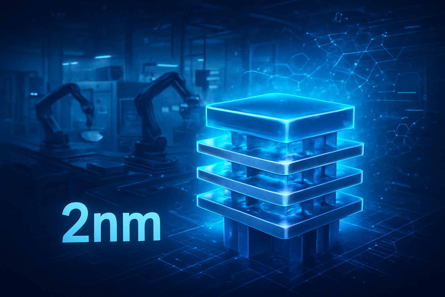
    In a move that signals a seismic shift in the global semiconductor landscape, Samsung Electronics (KRX: 005930) has officially commenced risk production for its 2nm (SF2) process node at its $44 billion facility in Taylor, Texas. This milestone marks the first time that cutting-edge 2nm-class silicon has been manufactured on U.S. soil, representing a critical victory for Samsung in its bid to challenge the dominance of Taiwan Semiconductor Manufacturing Company (TPE: 2330).

    The Taylor facility, which has transitioned from its original 4nm mandate to a "2nm-first" strategy, is now operating its first batch of advanced lithography systems. This development is not merely a technical achievement; it is a foundational pillar of the U.S. strategy to secure domestic leading-edge chip production. Supported by $6.4 billion in subsidies from the CHIPS and Science Act, Samsung’s Texas operations are now the epicenter of a "Turnkey" manufacturing ecosystem designed to provide the world’s most advanced AI hardware under one roof.

    Technical Prowess: Third-Generation GAA and CNT Pellicles

    The 2nm process, designated as SF2 by Samsung Foundry, utilizes the third generation of the company’s proprietary Gate-All-Around (GAA) architecture, branded as Multi-Bridge Channel FET (MBCFET). While competitors like TSMC are just beginning their transition to GAA at the 2nm level, Samsung is leveraging nearly four years of telemetry data from its early 3nm GAA production. The SF2 node delivers a 12% increase in performance and a 25% reduction in power consumption compared to the previous 3nm generation. This efficiency is critical for the next wave of hyperscale AI accelerators and mobile processors that are pushing the limits of thermal management.

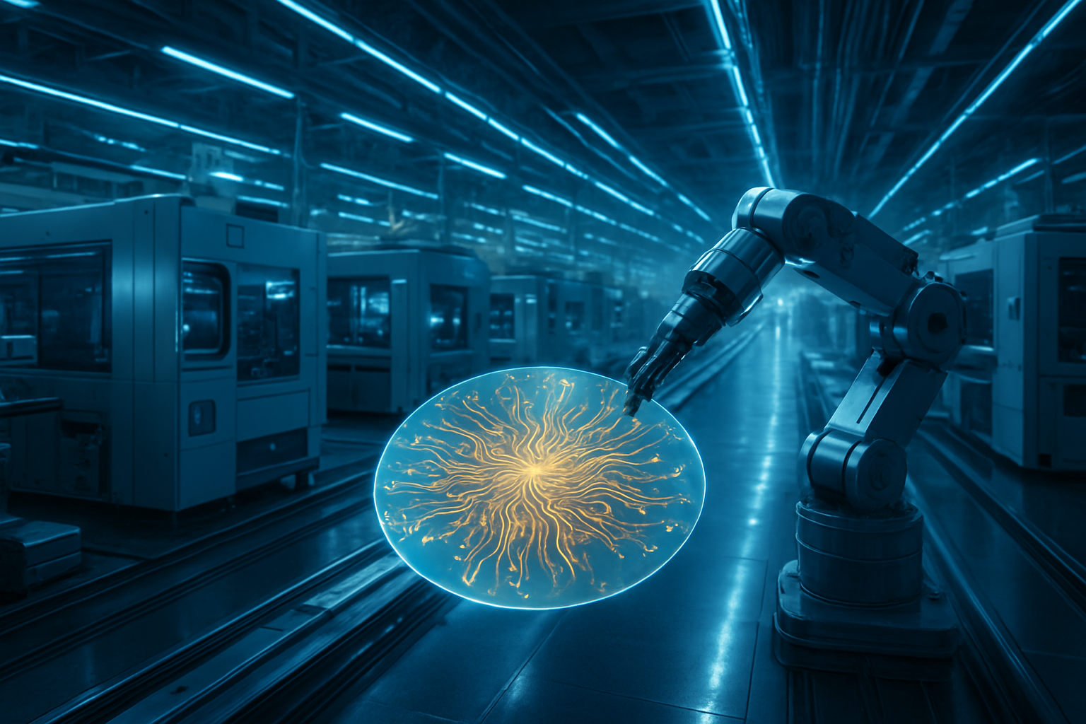
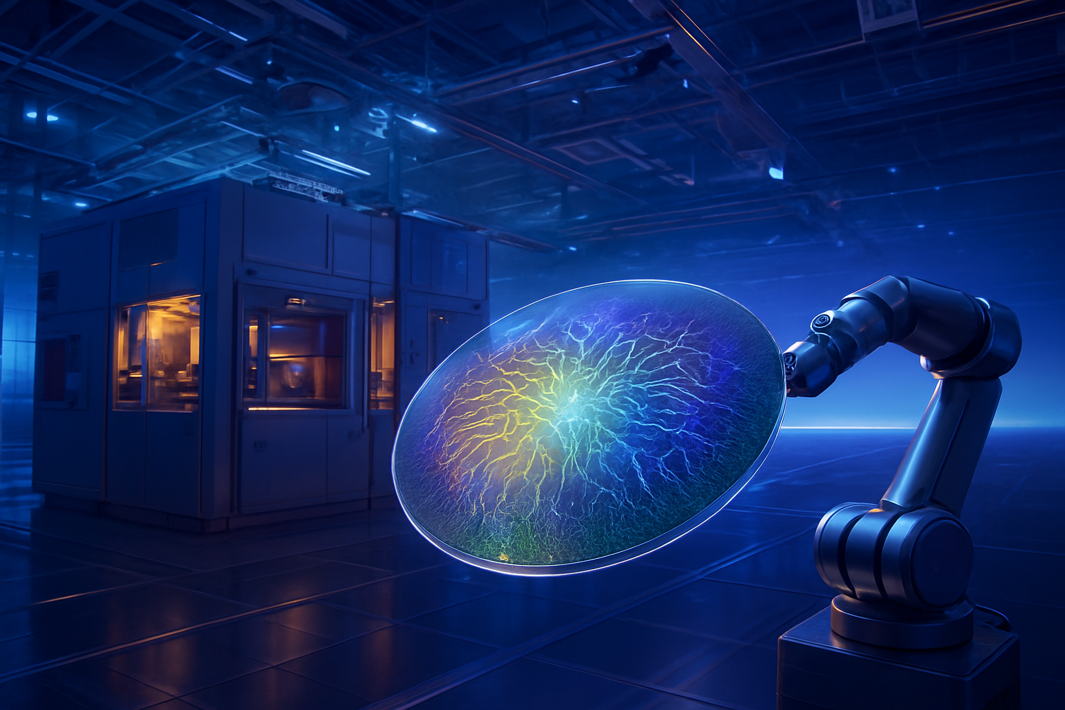
    A key differentiator in the Taylor fab’s 2nm line is the large-scale implementation of advanced Extreme Ultraviolet (EUV) pellicles. Samsung has adopted Carbon Nanotube (CNT) pellicle technology, which boasts a light transmittance rate exceeding 97%. This is a significant upgrade over traditional silicon-based pellicles, which often suffer from lower transparency and thermal degradation under the high-power EUV beams required for 2nm patterning. By reducing "stochastic" defects and increasing wafer throughput, these CNT pellicles are expected to help Samsung achieve a target yield of 60-70%—a figure that would make it highly competitive with TSMC’s N2 node.

    Furthermore, Samsung is preparing its SF2P (Performance) variant for high-end data center applications, which features specialized channel strain engineering to reduce parasitic capacitance. Initial reactions from the industry have been cautiously optimistic; while Samsung struggled with early 3nm yields, the stabilization of its 2nm process in Taylor suggests that the company has finally overcome the learning curve associated with GAA structures.

    Market Dynamics: Courting AMD, Qualcomm, and Tesla

    Samsung’s strategic pivot to the United States is already paying dividends in terms of customer acquisition. Advanced Micro Devices (NASDAQ: AMD) and Qualcomm (NASDAQ: QCOM) are reportedly in deep negotiations to secure 2nm capacity at the Taylor fab. For Qualcomm, the attraction lies in Samsung’s ability to offer a "dual-sourcing" alternative to TSMC, where Apple has reportedly reserved the lion's share of initial 2nm capacity. Industry insiders suggest that Samsung’s 2nm wafers could be priced as much as 33% lower than TSMC’s, providing a vital margin cushion for chip designers facing rising manufacturing costs.

    The Taylor fab has also secured a cornerstone client in Tesla (NASDAQ: TSLA). The electric vehicle giant is expected to use the facility for its next-generation AI6 autonomous driving chips. By fabbing these chips in Texas, Tesla gains a localized supply chain that minimizes geopolitical risk and logistical overhead. This "Made in USA" advantage is becoming a primary selling point as tech giants look to diversify their manufacturing footprint away from East Asia.

    The competitive landscape is further complicated by Intel (NASDAQ: INTC), which has recently ramped up its 18A node. While Intel currently holds a lead in backside power delivery technology, Samsung’s "Turnkey Strategy"—which integrates 2nm logic, HBM4 memory, and advanced 3D packaging (SAINT)—offers a comprehensive solution that Intel and TSMC struggle to match individually. This holistic approach is particularly attractive to AI startups and hyperscalers that require high-bandwidth memory to be stacked directly onto 2nm logic dies.

    Geopolitics and the AI Hardware Explosion

    The commencement of 2nm risk production in Taylor is a landmark moment in the broader AI landscape. As the demand for NVIDIA (NASDAQ: NVDA) GPUs and custom AI ASICs continues to outpace supply, the addition of a major 2nm hub in the United States provides a necessary safety valve for the industry. It aligns perfectly with the current trend toward sovereign AI, where nations and corporations seek to control their hardware destiny.

    This development also underscores the success of the CHIPS Act in incentivizing leading-edge manufacturing within the U.S. The Taylor campus, now a $44 billion investment, represents one of the largest foreign direct investments in U.S. history. By fostering a "K-Semiconductor Cluster" in Central Texas—including specialized suppliers for EUV pellicles and materials—Samsung is building an ecosystem that will likely influence semiconductor trends for the next decade.

    However, concerns remain regarding the speed of the yield ramp. While 60% yield is a strong start for 2nm, the industry standard for high-volume profitability typically requires upwards of 70-80%. Comparisons to previous milestones, such as the move from 7nm to 5nm, show that the transition to 2nm is orders of magnitude more complex due to the extreme precision required in lithography and the fragility of nanosheet structures.

    The Horizon: From Risk Production to 1.4nm

    Looking ahead, Samsung plans to transition from risk production to full-scale mass production at the Taylor fab by the second half of 2026. This timeline puts them in a neck-and-neck race with TSMC’s Arizona facility. In the near term, we can expect to see the first 2nm-powered consumer devices, likely headlined by Samsung's own Galaxy S27 series and potentially a refreshed line of AI-capable laptops from various OEMs.

    Beyond 2nm, Samsung has already laid out a roadmap for its 1.4nm (SF1.4) node, which is slated for development by late 2027. The Taylor fab is designed to be future-proof, with the infrastructure already in place to support the move to "High-NA" EUV systems from ASML (NASDAQ: ASML) as they become commercially viable. The primary challenge moving forward will be the integration of Backside Power Delivery (BSPDN) in the SF2Z variant, which experts predict will be the next major battleground in semiconductor architecture.

    A Final Assessment of the Taylor Milestone

    The commencement of 2nm risk production at Samsung’s Taylor fab is a definitive "coming of age" moment for the U.S. semiconductor industry and a bold statement of intent from Samsung. By combining its 3rd-generation GAA technology with a multi-billion dollar commitment to American manufacturing, Samsung is not just building a factory; it is attempting to rewrite the rules of the foundry market.

    The significance of this development in AI history cannot be overstated. As AI models become more complex, the hardware that powers them must become more efficient and accessible. The Taylor facility provides the capacity and the cutting-edge tech to meet that demand. In the coming weeks and months, the industry will be watching Samsung’s yield reports and customer announcements closely. If the company can maintain its current momentum, the "Silicon Hills" of Texas may soon become the most important real estate in the global AI economy.


    This content is intended for informational purposes only and represents analysis of current AI developments.

    TokenRing AI delivers enterprise-grade solutions for multi-agent AI workflow orchestration, AI-powered development tools, and seamless remote collaboration platforms.
    For more information, visit https://www.tokenring.ai/.

  • Glass Substrates: Intel and Samsung Pivot to Next-Gen AI Packaging

    Glass Substrates: Intel and Samsung Pivot to Next-Gen AI Packaging

    The semiconductor industry has reached a historic inflection point in early 2026 as the foundational materials of computing undergo their most significant change in decades. In a decisive pivot to meet the insatiable thermal and interconnect demands of generative artificial intelligence, industry titans Intel (Nasdaq: INTC) and Samsung Electronics (KRX: 005930) have officially commenced the transition from organic resin substrates to glass. This shift represents a fundamental redesign of the "brain" of the AI data center, moving away from the plastic-like materials that have dominated the industry for forty years toward a rigid, ultra-flat glass architecture capable of supporting the massive multi-chiplet arrays required by the next generation of Large Language Models (LLMs).

    The immediate significance of this move cannot be overstated. As AI accelerators push past the 1,000-watt power envelope, traditional organic substrates—primarily based on Ajinomoto Build-up Film (ABF)—have hit a "warpage wall." These legacy materials tend to bend and buckle under high heat, leading to connection failures and limiting the number of chiplets that can be stitched together. By adopting glass, manufacturers are effectively providing a "granite foundation" for silicon, enabling the construction of larger, more powerful, and more energy-efficient AI systems. Intel’s recent deployment of its first glass-core processors marks the beginning of an era where material science, rather than just transistor shrinking, dictates the pace of AI progress.

    The Technical Leap: Solving the Warpage Wall

    At the heart of this transition is the superior physical properties of glass compared to organic resins. Organic substrates possess a Coefficient of Thermal Expansion (CTE) that differs significantly from the silicon chips they support. When an AI chip heats up during training or inference, the organic board expands at a different rate than the silicon, causing the "potato-chip" effect—a warping that can crack microscopic solder bumps. Glass, however, can be engineered to match the CTE of silicon almost perfectly (3–5 ppm/°C). This allows for a 10x increase in interconnect density through the use of Through-Glass Vias (TGVs), which are vertical electrical connections drilled directly through the glass core.

    The flatness of glass is its other primary weapon. As of February 2026, Intel’s "Thick Core" glass substrates have demonstrated warpage levels of less than 20μm across a 100mm span, compared to over 50μm for high-end organic alternatives. This extreme flatness is critical for ultra-fine lithography; it allows engineers to pack more chiplets (GPUs, HBM memory, and I/O dies) closer together with tighter pitches. Furthermore, glass offers 60% lower dielectric loss, meaning signals travel faster and with significantly less power consumption—a vital metric for the high-bandwidth interconnects that link HBM4 memory to AI processing cores.

    Initial reactions from the AI research community have been overwhelmingly positive, though tempered by the logistical hurdles of high-volume manufacturing. Dr. Aris Thompson, a senior packaging analyst, noted that "the transition to glass is essentially the 'save game' for Moore’s Law." While organic substrates were reaching their physical limits at two reticle sizes, glass substrates are expected to support "System-in-Package" designs that are five to ten times larger than anything currently on the market. However, industry experts caution that yield rates remain the primary battleground, with current glass production yields hovering between 75% and 85%, significantly lower than the 95% maturity of the organic ecosystem.

    Competitive Landscapes and Strategic Alliances

    The race to dominate the glass substrate market has created a new competitive dynamic between Intel and Samsung. Intel (Nasdaq: INTC) currently holds the first-mover advantage, having integrated glass core technology into its newly launched Xeon 6+ "Clearwater Forest" processors manufactured in Chandler, Arizona. Intel’s strategy is not just internal; the company has begun licensing its portfolio of over 600 glass-related patents to specialist manufacturers like JNTC. By doing so, Intel is positioning itself as the "open standard" for glass packaging, hoping to entice AI giants like NVIDIA (Nasdaq: NVDA) and Apple (Nasdaq: AAPL) to utilize Intel Foundry services for their 2027 hardware cycles.

    Samsung Electronics (KRX: 005930) has responded with a formidable "Triple Alliance" across its internal divisions. Samsung Electro-Mechanics (SEMCO) is spearheading the substrate production, while Samsung Display is repurposing its expertise in high-precision glass handling from its OLED production lines. This vertical integration allows Samsung to control the entire value chain—from the raw glass panel to the final interposer. Samsung recently announced a joint venture with Sumitomo Chemical (TYO: 4005) to secure specialized glass core materials, a strategic move to insulate itself from the "Glass Cloth Crisis" currently affecting the global supply chain.

    This pivot places significant pressure on Taiwan Semiconductor Manufacturing Company (TSMC) (NYSE: TSM). While TSMC remains the undisputed leader in organic Chip-on-Wafer-on-Substrate (CoWoS) packaging, it has been forced to accelerate its own "Rectangular Revolution." TSMC is now fast-tracking its Fan-Out Panel-Level Packaging (FOPLP) on glass, with pilot lines expected to debut later this year. Meanwhile, smaller players like Absolics, a subsidiary of SKC, have completed high-volume facilities in Georgia, aiming to capture custom AI hardware contracts from AMD (Nasdaq: AMD) and Amazon (Nasdaq: AMZN) by the end of 2026.

    The Broader AI Landscape: Efficiency and Sustainability

    The shift to glass substrates is more than a technical footnote; it is a critical response to the environmental and economic pressures of the AI boom. As training LLMs becomes increasingly energy-intensive, the 50% reduction in power consumption for signal transmission offered by glass becomes a vital tool for sustainability. This development fits into the broader trend of "Advanced Packaging" becoming the primary driver of semiconductor performance, as traditional node shrinking becomes prohibitively expensive and physically difficult.

    However, the transition is not without concerns. The sudden surge in demand for high-grade "T-glass" cloth, essential for these substrates, has led to a market shortage. Suppliers like Nitto Boseki (TYO: 3110) are struggling to keep pace, leading to a bidding war between the major foundries. This "Glass Cloth Crisis" threatens to inflate the cost of AI hardware in the short term, potentially creating a bottleneck for startups and mid-sized AI labs that lack the purchasing power of "Big Tech."

    In historical context, the move to glass mirrors the industry’s transition from ceramic to organic substrates in the 1990s. Just as that shift enabled the rise of the personal computer and the mobile era, the move to glass is seen as the prerequisite for the "General AI" era. By allowing for larger and more complex chiplet architectures, glass substrates are enabling the hardware that will run the next generation of trillion-parameter models, which were previously constrained by the physical limits of organic packaging.

    Future Horizons: HBM4 and Beyond

    Looking ahead, the roadmap for glass substrates extends far beyond simple CPU and GPU cores. By 2028, experts predict that glass will be the primary material for the interposers used in HBM4 (High Bandwidth Memory). As memory stacks become taller and more dense, the thermal stability of glass will be essential to prevent heat from the logic die from degrading the memory’s performance. This will lead to AI accelerators that are not only faster but significantly more compact, potentially leading to "edge AI" servers with the power of today's massive data centers.

    We are also likely to see the emergence of optical interconnects integrated directly into the glass substrate. Because glass is transparent and can be etched with extreme precision, it is an ideal medium for co-packaged optics. This would allow for data to be moved via light rather than electricity between chips, virtually eliminating latency and further slashing power consumption. The long-term vision is a "universal substrate" where logic, memory, and high-speed networking are all fused onto a single, massive glass panel.

    The immediate challenge remains scaling. While Intel has proven mass production is possible with the Xeon 6+, scaling this to the millions of units required by the global AI market will require significant investment in new "Panel-Level" manufacturing equipment. Experts predict that 2026 will be the "Year of Validation," with 2027 and 2028 seeing a flood of glass-based AI products from every major hardware vendor.

    Summary and Final Thoughts

    The transition to glass substrates by Intel and Samsung marks a definitive end to the era of organic-dominated semiconductor packaging. By solving the critical issues of warpage, thermal management, and signal integrity, glass provides the necessary infrastructure for the next decade of AI growth. Intel’s early lead in Arizona and Samsung’s vertically integrated alliance represent two different paths to the same goal: providing the physical foundation for the most complex machines ever built.

    As we move through the first half of 2026, the key metrics to watch will be yield stability and the resolution of the glass cloth supply chain issues. For investors and industry observers, the performance of the Xeon 6+ in real-world AI workloads will be the first true test of this technology’s promise. If glass delivers on its potential to slash power while boosting interconnect density, the current "silicon gold rush" may soon be remembered as the "glass revolution."


    This content is intended for informational purposes only and represents analysis of current AI developments.

    TokenRing AI delivers enterprise-grade solutions for multi-agent AI workflow orchestration, AI-powered development tools, and seamless remote collaboration platforms.
    For more information, visit https://www.tokenring.ai/.

  • Intel 18A Node Reaches High-Volume Production in Arizona

    Intel 18A Node Reaches High-Volume Production in Arizona

    In a move that signals a tectonic shift in the global semiconductor landscape, Intel (NASDAQ: INTC) has officially commenced high-volume manufacturing (HVM) of its pioneering Intel 18A process node at its Ocotillo campus in Chandler, Arizona. This milestone marks the successful completion of CEO Pat Gelsinger’s audacious "5 nodes in 4 years" (5N4Y) roadmap, a strategic sprint designed to reclaim the company's manufacturing leadership after years of falling behind its Asian competitors. The 18A node, roughly equivalent to 1.8nm-class technology, is not just a hardware milestone; it is the foundational platform for the next generation of artificial intelligence, providing the power efficiency and transistor density required for advanced neural processing units (NPUs) and massive data center deployments.

    The immediate significance of this launch lies in Intel’s "first-mover" advantage with two revolutionary technologies: RibbonFET and PowerVia. By beating rivals Taiwan Semiconductor Manufacturing Co. (NYSE: TSM) and Samsung (KRX: 005930) to the implementation of backside power delivery at scale, Intel has positioned itself as the primary alternative for AI chip designers who are increasingly constrained by the thermal and power limits of traditional silicon architectures. As of early 2026, the 18A ramp is already supporting flagship products such as "Panther Lake" for AI PCs and "Clearwater Forest" for high-density server environments, effectively signaling that the "process gap" between Intel and the world's leading foundries has been closed.

    The Technical Frontier: RibbonFET and PowerVia

    The Intel 18A node represents the most significant architectural overhaul of the transistor since the introduction of FinFET in 2011. At the heart of this advancement is RibbonFET, Intel’s proprietary implementation of Gate-All-Around (GAA) technology. Unlike the previous FinFET design, where the gate only covers three sides of the channel, RibbonFET wraps the gate entirely around the silicon channel. This provides significantly better electrical control, reducing current leakage—a critical factor as transistors shrink toward the atomic scale—and allowing for higher drive currents that translate directly into faster switching speeds.

    Equally transformative is PowerVia, Intel’s breakthrough in backside power delivery. Traditionally, power lines and signal wires are woven together on the front side of a chip, leading to "wiring congestion" that slows down performance and generates excess heat. PowerVia separates these functions, moving the entire power delivery network to the back of the silicon wafer. Initial data from the Arizona HVM lines indicates that PowerVia reduces voltage droop by up to 30% and enables a 6% boost in clock frequencies at identical power levels compared to front-side delivery. This "de-cluttering" of the wafer's front side has also enabled Intel to achieve a transistor density of approximately 238 million transistors per square millimeter (MTr/mm²).

    The industry response to these technical specifications has been one of cautious optimism turning into a full-scale endorsement. Early yield reports from the Ocotillo fabs suggest that Intel has achieved a stable yield rate between 55% and 75% for 18A, a threshold that many analysts believed would take much longer to reach. Experts in the AI research community note that the 15% performance-per-watt improvement over the previous Intel 3 node is specifically optimized for "always-on" AI workloads, where efficiency is just as critical as raw throughput.

    Disrupting the Foundry Monopoly

    The successful launch of 18A in Arizona has profound implications for the global foundry market, where TSMC (NYSE: TSM) has long enjoyed a near-monopoly on the most advanced nodes. With 18A now in high-volume production, Intel Foundry is no longer a theoretical competitor but a tangible threat. Tech giants such as Microsoft (NASDAQ: MSFT) and Amazon (NASDAQ: AMZN) have already signed on as major 18A customers, seeking to leverage Intel’s domestic manufacturing footprint to secure their AI supply chains. For Microsoft, the 18A node will likely power future iterations of its custom Maia AI accelerators, reducing its total dependence on external foundries.

    The competitive pressure is now squarely on TSMC and Samsung. While TSMC’s N2 (2nm) node boasts a slightly higher raw transistor density, it lacks backside power delivery, a feature TSMC does not plan to integrate until its A16 node in late 2026 or early 2027. This gives Intel a temporary "feature lead" that is attracting designers of high-performance AI silicon who need the thermal benefits of PowerVia today. Samsung, despite being the first to market with GAA technology at 3nm, has reportedly struggled with yields on its SF2 (2nm) node, leaving an opening for Intel to capture the "Number Two" spot in the global foundry rankings.

    Furthermore, the 18A node’s integration with Intel’s Foveros Direct 3D packaging technology allows for the stacking of compute tiles directly on top of each other with copper-to-copper bonding. This allows startups and AI labs to design modular "chiplet" architectures that combine 18A logic with cheaper, mature nodes for I/O, drastically lowering the barrier to entry for custom AI silicon. By offering both the cutting-edge node and the advanced packaging in a single "systems foundry" approach, Intel is repositioning itself as a one-stop-shop for the AI era.

    A New Era for the AI Landscape

    The arrival of 18A marks a pivotal moment in the broader AI landscape, moving the industry away from "AI software optimization" and back toward "silicon-led innovation." As large language models (LLMs) continue to grow in complexity, the hardware bottleneck has become the primary constraint for AI development. Intel 18A directly addresses this by providing the thermal headroom necessary for more aggressive NPU designs. This development fits into a larger trend of "Sovereign AI," where nations and corporations seek to control their own hardware destiny to ensure security and supply stability.

    The geopolitical significance of the Arizona production cannot be overstated. By achieving HVM of 18A on U.S. soil, Intel is fulfilling a core objective of the CHIPS and Science Act, providing a secure, leading-edge domestic supply of the chips that power critical infrastructure and defense systems. This creates a "silicon shield" for the U.S. tech industry, mitigating the risks associated with the geographic concentration of semiconductor manufacturing in East Asia.

    However, the rapid transition to 1.8nm-class technology also raises concerns regarding the environmental footprint of such advanced manufacturing. The extreme ultraviolet (EUV) lithography required for 18A is immensely energy-intensive. Intel has countered these concerns by committing to 100% renewable energy use at its Ocotillo campus by 2030, but the sheer scale of the 18A ramp-up will be a test for the company’s sustainability goals. Compared to previous milestones like the move to 10nm, the 18A launch is characterized by its focus on "performance-per-watt" rather than just "more transistors," reflecting the energy-hungry reality of modern AI.

    The Road to 14A and Beyond

    Looking ahead, the high-volume production of 18A is merely the beginning of Intel’s long-term roadmap. The company is already looking toward Intel 14A, which will introduce High-NA (Numerical Aperture) EUV lithography to further push the boundaries of miniaturization. Expected to enter risk production in late 2026 or early 2027, 14A will build upon the RibbonFET and PowerVia foundation established by 18A. In the near term, the industry will be watching the market reception of "Panther Lake" CPUs, which will serve as the first major commercial test of 18A’s performance in the hands of consumers.

    Future applications on the horizon include "Edge AI" devices that can run complex generative models locally without needing a cloud connection. The efficiency gains of 18A are expected to enable 24-hour battery life on AI-enhanced laptops and more sophisticated autonomous vehicle controllers that can process sensor data with minimal latency. Challenges remain, particularly in scaling the production of Foveros Direct packaging and managing the complex supply chain for the rare materials required for 1.8nm features, but experts predict that Intel’s successful 5N4Y execution has restored the "tick-tock" rhythm of innovation that the company was once famous for.

    Summary and Final Thoughts

    The start of high-volume production for Intel 18A in Arizona is more than just a company milestone; it is a signal that the era of uncontested dominance by a single foundry is over. By delivering on the "5 nodes in 4 years" promise, Intel has re-established its technical credibility and provided the AI industry with a powerful new toolkit. The combination of RibbonFET and PowerVia offers a glimpse into the future of semiconductor physics, where performance is derived from clever 3D architecture as much as it is from shrinking dimensions.

    As we move further into 2026, the success of 18A will be measured by its ability to win over the "hyperscalers" and maintain its yield advantage over TSMC’s upcoming 2nm offerings. For the first time in a decade, the silicon crown is up for grabs, and Intel has officially entered the ring. Investors and tech enthusiasts should watch for upcoming quarterly reports to see how 18A orders from external foundry customers are scaling, as these will be the ultimate barometer of Intel's long-term resurgence in the AI-driven economy.


    This content is intended for informational purposes only and represents analysis of current AI developments.

    TokenRing AI delivers enterprise-grade solutions for multi-agent AI workflow orchestration, AI-powered development tools, and seamless remote collaboration platforms.
    For more information, visit https://www.tokenring.ai/.

  • Samsung Hits 70% Yield on 2nm GAA (SF2P): A Turning Point for the AI Chip Supply Chain

    Samsung Hits 70% Yield on 2nm GAA (SF2P): A Turning Point for the AI Chip Supply Chain

    As of January 30, 2026, the global semiconductor landscape is undergoing a tectonic shift. Samsung Electronics (KRX: 005930) has officially reached a critical performance and yield milestone for its 2nm (SF2P) production process, signaling a major challenge to the long-standing dominance of Taiwan Semiconductor Manufacturing Company (NYSE: TSM). Following its Q4 2025 earnings report, Samsung confirmed that its performance-optimized 2nm node, known as SF2P, has successfully hit the 70% yield threshold required for stable mass production—a feat that many industry skeptics thought would take years to master.

    This development is more than just a technical victory; it is a strategic lifeline for the world’s largest chip designers. With TSMC’s 2nm capacity currently overwhelmed by exclusive orders from high-priority clients, the emergence of a viable, high-yield alternative from Samsung provides a release valve for a supply chain that has been dangerously bottlenecked. By mastering the intricate Gate-All-Around (GAA) architecture ahead of its rivals, Samsung is positioning itself as the primary destination for the next generation of high-performance AI and mobile processors.

    Engineering the Future: The Maturity of 3rd-Gen GAA

    The SF2P node represents the second generation of Samsung’s 2nm platform, specifically optimized for high-performance computing (HPC) and premium mobile devices. Unlike traditional FinFET transistors, which hit physical scaling limits years ago, Samsung’s 2nm utilizes its proprietary Multi-Bridge Channel FET (MBCFET) architecture—a 3rd-generation evolution of GAA technology. This approach allows for a "nanosheet" design where the width of the channel can be adjusted to optimize for either extreme power efficiency or maximum performance. Compared to the first-generation SF2 node, the 2026-era SF2P delivers a 12% boost in clock speeds, a 25% improvement in power efficiency, and an 8% reduction in total die area.

    Technical experts note that Samsung’s early gamble on GAA—which it first introduced at the 3nm node while TSMC stuck with FinFET—is finally paying dividends. While competitors are only now navigating the "learning curve" of nanosheet production, Samsung has accumulated four years of telemetry data on GAA manufacturing. This experience has allowed the foundry to refine its extreme ultraviolet (EUV) lithography processes and address the "stochastic" defects that typically plague sub-3nm nodes. The result is a more uniform transistor structure that significantly reduces leakage current, a critical requirement for the power-hungry AI workloads of 2026.

    A Strategic Pivot: Qualcomm and AMD Secure Capacity

    The immediate beneficiaries of Samsung’s yield breakthrough are Qualcomm (NASDAQ: QCOM) and AMD (NASDAQ: AMD). As of late January 2026, both companies are reportedly in final negotiations to shift significant portions of their 2nm roadmap to Samsung Foundry. The move is driven by a stark reality: TSMC’s 2nm (N2) capacity is nearly 50% reserved by a single customer, leaving other tech giants fighting for leftovers and paying a "wafer premium" that has risen 50% over previous generations. Qualcomm is expected to utilize SF2P for its next-generation Snapdragon series, while AMD is eyeing the node for its "Venice" EPYC server CPUs to ensure supply stability in the face of skyrocketing enterprise demand.

    This shift represents a significant competitive disruption. For years, TSMC’s "foundry-only" model gave it a reputation for neutrality and reliability that Samsung, a conglomerate that also makes its own consumer products, struggled to match. However, the sheer scale of the AI boom has forced a "dual-sourcing" strategy among major chip designers. By offering competitive yields and more favorable pricing than TSMC, Samsung is transforming the foundry market from a monopoly into a true duopoly. Furthermore, Samsung’s massive $16.5 billion contract with Tesla (NASDAQ: TSLA) for its AI6 autonomous driving chips has served as a powerful "seal of approval," encouraging other automotive and data center players to reconsider their reliance on a single supplier.

    The "One-Stop" AI Solution and the Taylor, Texas Factor

    Samsung’s 2nm success is part of a broader "total solution" strategy that integrates logic, memory, and packaging. In January 2026, Samsung began large-scale shipments of its 12-layer HBM4 (High Bandwidth Memory), a key component for AI accelerators used by NVIDIA (NASDAQ: NVDA) and others. By offering 2nm logic manufacturing alongside HBM4 and advanced X-Cube 3D packaging, Samsung provides a vertically integrated stack that reduces latency and power consumption. This "one-stop shop" capability is something neither TSMC nor Intel (NASDAQ: INTC) can currently match with the same level of internal synchronization, making Samsung an attractive partner for startups building custom "Agentic AI" silicon.

    The geopolitical dimension of this ramp-up cannot be ignored. Samsung’s Taylor, Texas facility is now 93% complete and is transitioning to a "2nm-first" factory. With trial runs of ASML EUV lithography tools scheduled for March 2026, the Taylor fab is set to become a cornerstone of the "Made in USA" advanced chip initiative. This domestic capacity is a major selling point for U.S.-based companies like AMD and Google, who are under increasing pressure to diversify their manufacturing away from the geopolitical sensitivities of the Taiwan Strait. Samsung’s ability to hit 70% yield in its Korean facilities provides the blueprint for a rapid and successful ramp in the United States.

    Looking Ahead: The Road to 1.4nm and Backside Power

    While the industry focuses on the SF2P ramp, Samsung’s R&D teams are already moving toward the next frontier. Near-term developments include the introduction of SF2Z in 2027, which will incorporate Backside Power Delivery Network (BSPDN) technology. This innovation moves the power circuitry to the back of the wafer, freeing up the top side for more transistors and further reducing voltage drops. Beyond 2nm, the roadmap points toward the 1.4nm (SF1.4) node, where Samsung expects to apply lessons from its GAA maturity to achieve even more aggressive density gains.

    The challenge remains in maintaining these yields as the volume scales to hundreds of thousands of wafers per month. Experts predict that the next 12 months will be a "volume war" as Samsung attempts to match the total output capacity of TSMC’s sprawling "GigaFabs." Additionally, as AI models move from data centers to "on-device" edge environments, the demand for SF2P-class chips will expand into a wider variety of form factors, including wearable AR glasses and advanced robotics. The primary hurdle will be the continued availability of high-NA EUV tools and the specialized gases required for sub-2nm etching.

    A New Era for the Semiconductor Industry

    Samsung’s achievement of 70% yield on the SF2P node marks a historic comeback for the South Korean giant. After years of trailing TSMC in the transition from 7nm to 5nm and 4nm, Samsung has utilized the radical architecture shift of Gate-All-Around to leapfrog its competition in terms of manufacturing maturity. This development effectively breaks the "TSMC bottleneck," providing the global AI industry with the diversified supply chain it desperately needs to sustain its current pace of innovation.

    In the coming weeks, the industry will be watching for the official "tape-out" announcements from Qualcomm and AMD, which will confirm the first commercial products to use this new technology. The successful integration of SF2P into the global supply chain will not only redefine Samsung’s financial trajectory but will also serve as a catalyst for more affordable and efficient AI hardware worldwide. As we move deeper into 2026, the foundry race has officially been reset, and for the first time in a decade, the lead is up for grabs.


    This content is intended for informational purposes only and represents analysis of current AI and semiconductor developments.

    TokenRing AI delivers enterprise-grade solutions for multi-agent AI workflow orchestration, AI-powered development tools, and seamless remote collaboration platforms.
    For more information, visit https://www.tokenring.ai/.

  • Samsung’s HBM4 Breakthrough: NVIDIA and AMD Clearance Signals New Era in AI Memory

    Samsung’s HBM4 Breakthrough: NVIDIA and AMD Clearance Signals New Era in AI Memory

    In a decisive move that reshapes the competitive landscape of artificial intelligence infrastructure, Samsung Electronics (KRX: 005930) has officially cleared the final quality and reliability tests for its 6th-generation High Bandwidth Memory (HBM4) from both NVIDIA (NASDAQ: NVDA) and AMD (NASDAQ: AMD). As of late January 2026, this breakthrough signals a major reversal of fortune for the South Korean tech giant, which had spent much of the previous two years trailing behind its chief rival, SK Hynix (KRX: 000660), in the race to supply the memory chips essential for generative AI.

    The validation of Samsung’s HBM4 is not merely a logistical milestone; it is a technological leap that promises to unlock the next tier of AI performance. By securing approval for NVIDIA’s upcoming "Vera Rubin" platform and AMD’s MI450 accelerators, Samsung has positioned itself as a critical pillar for the 2026 AI hardware cycle. Industry insiders suggest that the successful qualification has already led to the conversion of multiple production lines at Samsung’s P4 and P5 facilities in Pyeongtaek to meet the explosive demand from hyperscalers like Google and Microsoft.

    Technical Specifications: The 11Gbps Frontier

    The defining characteristic of Samsung’s HBM4 is its unprecedented data transfer rate. While the industry standard for HBM3E hovered around 9.2 to 10 Gbps, Samsung’s latest modules have achieved stable speeds of 11.7 Gbps per pin. This 11Gbps+ threshold is achieved through the implementation of Samsung’s 6th-generation 10nm-class (1c) DRAM process. This marks the first time a memory manufacturer has successfully integrated 1c DRAM into an HBM stack, providing a 20% improvement in power efficiency and significantly higher bit density than the 1b DRAM currently utilized by competitors.

    Unlike previous generations, HBM4 features a fundamental architectural shift: the integration of a logic base die. Samsung has leveraged its unique position as the world’s only company with both leading-edge memory and foundry capabilities to produce a "turnkey" solution. Utilizing its own 4nm foundry process for the logic die, Samsung has eliminated the need to outsource to third-party foundries like TSMC. This vertical integration allows for tighter architectural optimization, superior thermal management, and a more streamlined supply chain, addressing the heat dissipation issues that have plagued high-density AI memory stacks in the past.

    Initial reactions from the AI research community and semiconductor analysts have been overwhelmingly positive. "Samsung’s move to a 4nm logic die in-house is a game-changer," noted one senior analyst at the Silicon Valley Semiconductor Institute. "By controlling the entire stack from the DRAM cells to the logic interface, they have managed to reduce latency and power draw at a level that was previously thought impossible for 12-layer and 16-layer stacks."

    Market Displacement: Closing the Gap with SK Hynix

    For the past three years, SK Hynix has enjoyed a near-monopoly on the high-end HBM market, particularly through its exclusive "One-Team" alliance with NVIDIA. However, Samsung’s late-January breakthrough has effectively ended this era of undisputed dominance. While SK Hynix still holds a projected 54% market share for 2026 due to earlier contract wins, Samsung is aggressively clawing back territory, targeting a 30% or higher share by the end of the fiscal year.

    The competitive implications for the "Big Three"—Samsung, SK Hynix, and Micron (NASDAQ: MU)—are profound. Samsung’s ability to clear tests for both NVIDIA and AMD simultaneously creates a supply cushion for AI chipmakers who have been desperate to diversify their sources. For AMD, Samsung’s HBM4 is the "secret sauce" for the MI450, allowing them to offer a competitive alternative to NVIDIA’s Vera Rubin platform in terms of raw memory bandwidth. This shift prevents a single-supplier bottleneck, which has historically inflated prices for data center operators.

    Strategic advantages are also shifting toward a multi-vendor model. Tech giants like Meta and Amazon are reportedly pivoting their procurement strategies to favor Samsung’s turnkey solution, which offers a faster time-to-market compared to the collaborative Hynix-TSMC model. This diversification is seen as a vital step in stabilizing the global AI supply chain, which remains under immense pressure as LLM (Large Language Model) training requirements continue to scale exponentially.

    Broader Significance: The Vera Rubin Era and Global Supply

    The timing of Samsung’s breakthrough is meticulously aligned with the broader AI landscape's transition to "Hyper-Scale" inference. As the industry moves toward NVIDIA’s Vera Rubin architecture, the demand for memory bandwidth has nearly doubled. A Rubin-based system equipped with eight stacks of Samsung’s HBM4 can reach an aggregate bandwidth of 22 TB/s. This allows for the real-time processing of models with tens of trillions of parameters, effectively moving the needle from "generative chat" to "autonomous reasoning agents."

    However, this milestone also brings potential concerns to the forefront. The sheer volume of capacity required for HBM4 production has led to a "cannibalization" of standard DRAM production lines. As Samsung and SK Hynix shift their focus to AI memory, prices for consumer-grade DDR5 and mobile LPDDR6 are expected to rise sharply in late 2026. This highlights a growing divide between the AI-industrial complex and the consumer electronics market, where AI-specific hardware is increasingly prioritized over general-purpose computing.

    Comparatively, this milestone is being likened to the transition from 2D to 3D NAND flash a decade ago. It represents a "point of no return" where memory is no longer a passive storage component but an active participant in the compute cycle. The integration of logic directly into the memory stack signifies the first major step toward "Processing-in-Memory" (PIM), a long-held dream of computer scientists that is finally becoming a commercial reality.

    Future Outlook: Mass Production and GTC 2026

    The immediate next step for Samsung is the official public debut of the HBM4 modules at NVIDIA GTC 2026, scheduled for March 16–19. This event is expected to feature live demonstrations of the Vera Rubin platform, with Samsung’s memory powering the world’s most advanced AI training clusters. Following the debut, full-scale mass production is slated to ramp up in the second quarter of 2026, with the first server systems reaching hyperscale customers by August.

    Looking further ahead, experts predict that Samsung will use its current momentum to fast-track the development of HBM4E (Enhanced). While HBM4 is just entering the market, the roadmap for 2027 already includes 20-layer stacks and even higher clock speeds. The challenge remains in maintaining yields; at 11.7 Gbps, the margin for error in the Through-Silicon Via (TSV) manufacturing process is razor-thin. If Samsung can maintain its current yield rates as it scales, it could potentially reclaim the title of the world’s leading HBM supplier by 2027.

    A New Chapter in the AI Memory War

    In summary, Samsung’s successful navigation of the NVIDIA and AMD qualification process marks a historic comeback. By delivering 11Gbps speeds and a vertically integrated 4nm logic die, Samsung has proved that its "all-under-one-roof" strategy is a viable—and perhaps superior—alternative to the collaborative models of its rivals. This development ensures that the AI industry has the memory bandwidth necessary to power the next generation of reasoning-capable artificial intelligence.

    In the coming weeks, the industry will be watching for the official pricing structures and the first performance benchmarks of the Vera Rubin platform at GTC 2026. While SK Hynix remains a formidable opponent with deep ties to the AI ecosystem, Samsung has officially closed the gap, turning a one-horse race into a high-speed pursuit that will define the future of computing for years to come.


    This content is intended for informational purposes only and represents analysis of current AI developments.

    TokenRing AI delivers enterprise-grade solutions for multi-agent AI workflow orchestration, AI-powered development tools, and seamless remote collaboration platforms.
    For more information, visit https://www.tokenring.ai/.

  • SK Hynix Emerges as Indisputable “AI Memory King” with 70% Share of NVIDIA’s HBM4 Orders for “Vera Rubin” Platform

    SK Hynix Emerges as Indisputable “AI Memory King” with 70% Share of NVIDIA’s HBM4 Orders for “Vera Rubin” Platform

    In a seismic shift for the semiconductor industry, SK Hynix (KRX: 000660) has reportedly secured more than 70% of NVIDIA’s (NASDAQ: NVDA) initial orders for next-generation HBM4 memory, destined for the highly anticipated "Vera Rubin" AI platform. This development, confirmed in late January 2026, marks a historic consolidation of the high-bandwidth memory (HBM) market. By locking in the lion's share of NVIDIA's supply chain for the 2026-2027 cycle, SK Hynix has effectively sidelined its primary competitors, creating a widening gap in the race to power the world’s most advanced generative AI models.

    The announcement comes on the heels of SK Hynix’s record-shattering Q4 2025 financial results, which saw the company’s annual operating profit surpass that of industry titan Samsung Electronics (KRX: 005930) for the first time in history. With an operating margin of 58.4% in the final quarter of 2025, SK Hynix has demonstrated that specialized AI silicon is now more lucrative than the high-volume, general-purpose DRAM market that Samsung has dominated for decades. The "Vera Rubin" platform, utilizing SK Hynix’s advanced 12-layer and 16-layer HBM4 stacks, is expected to set a new benchmark for exascale computing and large-scale inference.

    The Architectural Shift: HBM4 and the "One Team" Alliance

    The move to HBM4 represents the most significant architectural evolution in memory technology since the inception of the HBM standard. Unlike HBM3E, which utilized a 1024-bit interface, HBM4 doubles the bus width to a 2048-bit I/O interface. This allows for staggering data throughput of over 2.0 TB/s per stack at lower clock speeds, drastically improving power efficiency—a critical factor for data centers already pushed to their thermal limits. SK Hynix’s HBM4 utilizes a "custom HBM" (cHBM) approach, where the traditional DRAM base die is replaced with a logic die manufactured using TSMC’s (NYSE: TSM) 12nm and 5nm processes. This integration allows for memory controllers and physical layer (PHY) functions to be embedded directly into the stack, reducing latency by an estimated 20%.

    NVIDIA’s "Vera Rubin" platform is designed to take full advantage of these technical leaps. The platform features the new Vera CPU—powered by 88 custom-designed Armv9.2 "Olympus" cores—and the Rubin GPU, which boasts 288GB of HBM4 memory per unit. This configuration provides a 5x increase in AI inference performance compared to the previous Blackwell architecture. Industry experts have noted that SK Hynix’s ability to mass-produce 16-high HBM4 modules, which thin individual DRAM dies to just 30 micrometers to maintain a standard 775-micrometer height limit, was the "killer app" that secured the NVIDIA contract.

    The success of SK Hynix is deeply intertwined with its "One Team" alliance with TSMC. By leveraging TSMC’s advanced packaging and logic processes for the HBM4 base die, SK Hynix has solved complex heat and signaling issues that have reportedly hampered its rivals. Initial reactions from the AI research community suggest that the HBM4-equipped Rubin systems will be the first to realistically support the real-time training of trillion-parameter models without the prohibitive energy costs associated with current-gen hardware.

    Market Dominance and the Competitive Fallout

    The implications for the competitive landscape are profound. For the fiscal year 2025, SK Hynix reported a staggering annual operating profit of 47.2 trillion won, edging out Samsung’s 43.6 trillion won. This reversal of fortunes highlights a fundamental change in the memory industry: value is no longer in sheer volume, but in high-performance specialization. While Samsung still leads in total DRAM production, its late entry into the HBM4 validation process allowed SK Hynix to capture the most profitable segment of the market. Although Samsung reportedly passed NVIDIA's quality tests in January 2026 and plans to begin mass production in February, it finds itself fighting for the remaining 30% of the Rubin supply chain.

    Micron Technology (NASDAQ: MU) remains a formidable third player, having successfully delivered 16-high HBM4 samples to NVIDIA and claiming that its 2026 capacity is already "pre-sold." However, Micron lacks the massive production scale of its Korean rivals. Market share projections for 2026 now place SK Hynix at 54% of the global HBM market, with Samsung at 28% and Micron at 18%. This dominance gives SK Hynix unprecedented leverage over pricing and roadmap alignment with the world’s leading AI chipmaker.

    Startups and smaller AI labs may feel the pinch of this consolidation. With SK Hynix’s entire 2026 HBM4 capacity already reserved by NVIDIA and a handful of hyperscalers like Google and AWS, the "compute divide" is expected to widen. Companies without pre-existing supply agreements may face multi-month lead times or exorbitant secondary-market pricing for the Rubin-based systems necessary to remain competitive in the frontier model race.

    Wider Significance in the AI Landscape

    The emergence of SK Hynix as a specialized powerhouse signals a broader trend in the AI landscape: the "logic-ization" of memory. As AI models become more data-hungry, the bottleneck has shifted from raw compute power to the speed at which data can be fed into the processor. By integrating logic functions into the memory stack via HBM4, the industry is moving toward a more holistic, system-on-package (SoP) approach to hardware design. This effectively blurs the line between memory and processing, a milestone that some experts believe is essential for achieving Artificial General Intelligence (AGI).

    Furthermore, the "Vera Rubin" platform’s emphasis on power efficiency reflects the industry's response to mounting environmental and regulatory concerns. As global data center energy consumption continues to skyrocket, the 30% power savings offered by HBM4’s wider, slower interface are no longer a luxury but a requirement for future scaling. This transition matches the trajectory of previous AI breakthroughs, such as the shift from CPUs to GPUs, by prioritizing specialized architectures over general-purpose flexibility.

    However, this concentration of power in the hands of a few—NVIDIA, SK Hynix, and TSMC—raises concerns regarding supply chain resilience. The "Vera Rubin" platform's reliance on this specific trifecta of companies creates a single point of failure for the global AI economy. Any geopolitical tension or manufacturing hiccup within this tightly coupled ecosystem could stall AI development globally, prompting calls from some Western governments for a more diversified domestic HBM supply chain.

    Future Developments and the Road to Rubin Ultra

    Looking ahead, the road is already paved for the next iteration of memory technology. While HBM4 is only just reaching the market, SK Hynix and NVIDIA are already discussing "HBM4E," which is expected to debut with the "Rubin Ultra" variant in late 2027. This successor is anticipated to scale to 1TB of memory per GPU, further pushing the boundaries of what is possible in large-scale inference and multi-modal AI.

    The immediate challenge for SK Hynix will be maintaining its yield rates as it scales 16-layer production. Thining silicon dies to 30 micrometers is a feat of engineering that leaves little room for error. If the company can maintain its current 70% share while improving yields, it could potentially reach operating margins that rival software companies. Meanwhile, the AI industry is watching closely for the emergence of "Processing-in-Memory" (PIM), where AI calculations are performed directly within the HBM stack. This could be the next major frontier for the SK Hynix-TSMC partnership.

    Summary of the New Silicon Hierarchy

    The report that SK Hynix has secured 70% of the HBM4 orders for NVIDIA’s Vera Rubin platform cements a new hierarchy in the semiconductor world. By pivoting early and aggressively toward high-bandwidth memory and forming a strategic "One Team" with TSMC, SK Hynix has transformed from a commodity memory supplier into a foundational pillar of the AI revolution. Its record 2025 profits and the displacement of Samsung as the profitability leader underscore a permanent shift in how value is captured in the silicon industry.

    As we move through the first quarter of 2026, the focus will shift to the real-world performance of the Vera Rubin systems. The ability of SK Hynix to deliver on its massive order book will determine the pace of AI advancement for the next two years. For now, the "AI Memory King" wears the crown securely, having successfully navigated the transition to HBM4 and solidified its status as the primary engine behind the exascale AI era.


    This content is intended for informational purposes only and represents analysis of current AI developments.

    TokenRing AI delivers enterprise-grade solutions for multi-agent AI workflow orchestration, AI-powered development tools, and seamless remote collaboration platforms.
    For more information, visit https://www.tokenring.ai/.

  • Silicon’s Next Giant Leap: TSMC Commences High-Volume 2nm Production as the Global AI Arms Race Intensifies

    Silicon’s Next Giant Leap: TSMC Commences High-Volume 2nm Production as the Global AI Arms Race Intensifies

    In a move that signals a tectonic shift in the global semiconductor landscape, Taiwan Semiconductor Manufacturing Company (TSMC) (NYSE: TSM) has officially entered high-volume manufacturing (HVM) for its N2 (2-nanometer) technology node as of January 2026. This milestone, centered at the company’s massive Fab 20 facility in Hsinchu’s Baoshan District, marks the first commercial deployment of Nanosheet Gate-All-Around (GAA) transistors—a radical departure from the FinFET architecture that has dominated the industry for over a decade.

    The commencement of N2 production is not merely a routine upgrade; it is the cornerstone of the next generation of artificial intelligence. As the world’s most advanced foundry ships its first batch of 2nm silicon to lead customers like Apple (NASDAQ: AAPL) and NVIDIA (NASDAQ: NVDA), the implications for AI efficiency and compute density are profound. With initial yields reportedly exceeding internal targets, the 2nm era has moved from the laboratory to the factory floor, promising to redefine the performance-per-watt metrics that govern the future of data centers and edge devices alike.

    The Nanosheet Revolution: Inside the Architecture of N2

    The transition to N2 represents the most significant technical hurdle TSMC has cleared since the introduction of FinFET at the 22nm node. Unlike the "fin" structure where the gate wraps around three sides of the channel, the Nanosheet GAA architecture allows the gate to completely surround the channel on all four sides. This "Gate-All-Around" configuration provides superior electrostatic control, which is essential for managing the current leakage that plagued previous nodes at smaller scales. By drastically reducing this "leakage power," TSMC has achieved a staggering 25% to 30% improvement in power efficiency compared to the N3E (3nm) node at the same speed.

    Beyond raw efficiency, N2 introduces a breakthrough "NanoFlex" technology. This capability allows chip designers to mix and match different nanosheet cell types—some optimized for high-density and others for high-performance—within a single chip layout. This granular control is particularly vital for AI accelerators and mobile processors, where different sections of the silicon must handle radically different workloads simultaneously. Initial reactions from the hardware engineering community have been overwhelmingly positive, with experts noting that the 10% to 15% speed increase at constant power will allow the next generation of smartphones to run complex, on-device Large Language Models (LLMs) without the thermal throttling that hampered 3nm devices.

    Production is currently anchored at Fab 20 in Hsinchu, often referred to as TSMC’s "mother fab" for the 2nm era. The facility is a marvel of modern engineering, utilizing the latest Extreme Ultraviolet (EUV) lithography tools with high numerical aperture (High-NA) capabilities being phased in for future iterations. While the N2 node currently utilizes traditional front-side power delivery, it lays the groundwork for the N2P and A16 (1.6nm) nodes, which will eventually introduce backside power delivery to further optimize signal integrity and power distribution.

    The 2nm Race: Competitive Dynamics and Market Hegemony

    The start of N2 HVM places TSMC in a fierce "three-way sprint" against Intel (NASDAQ: INTC) and Samsung (KRX: 005930). While Intel recently claimed it reached HVM for its 18A (1.8nm) node in late 2025, TSMC’s N2 is widely viewed by industry analysts as the "gold standard" for yield and reliability. Intel’s 18A employs a similar RibbonFET architecture and has taken an aggressive lead by integrating "PowerVia" backside power delivery early. However, TSMC’s massive ecosystem of IP partners and its established track record of delivering millions of wafers to Apple give it a strategic moat that competitors struggle to breach.

    The primary beneficiaries of this rollout are the titans of the AI and mobile sectors. Apple has reportedly secured the vast majority of the initial N2 capacity for its upcoming "A20" chips, which will likely power the next iteration of the iPhone. For NVIDIA, the shift to 2nm is critical for its Blackwell successors and future AI GPUs, where every percentage point of power efficiency translates into billions of dollars in savings for hyperscale data center operators like Microsoft (NASDAQ: MSFT) and Amazon (NASDAQ: AMZN). By maintaining its lead in HVM, TSMC reinforces its position as the indispensable bottleneck—and enabler—of the global AI economy.

    Samsung, meanwhile, is attempting to pivot by moving its 2nm production to its new facility in Taylor, Texas. This move is designed to capture the growing demand for "on-shore" manufacturing in the United States. However, with TSMC’s Fab 20 now pumping out 2nm wafers at scale in Taiwan, Samsung faces immense pressure to prove that its third-generation GAA process can match the "Golden Yields" that have become TSMC’s hallmark. The competition is no longer just about who has the smallest transistor, but who can manufacture it at the highest volume with the fewest defects.

    Global Implications: Geopolitics and the AI Scaling Law

    The launch of N2 production in Hsinchu reinforces Taiwan’s status as the "Silicon Shield" of the global economy. As AI models require exponentially more compute power to train and deploy, the physical limits of silicon were beginning to look like a ceiling. TSMC’s successful transition to GAA nanosheets effectively pushes that ceiling higher, providing the hardware foundation for the "Scaling Laws" that drive AI progress. The 30% reduction in power consumption is particularly significant in an era where power grid constraints have become the primary limiting factor for massive AI clusters.

    However, the concentration of such critical technology in a single geographic region remains a point of concern for global supply chain resilience. While TSMC is expanding its footprint in Arizona and Japan, the most advanced 2nm "mother fab" remains in Taiwan. This creates a strategic paradox: while the world depends on N2 to fuel the AI revolution, that revolution remains tethered to the stability of the Taiwan Strait. This has led to intensified efforts by the U.S. and EU to incentivize domestic leading-edge capacity, though as of early 2026, TSMC’s Hsinchu operations remain years ahead of any foreign alternatives.

    Comparing this milestone to previous breakthroughs, such as the move to FinFET in 2012, the N2 transition is arguably more complex. The move to GAA requires entirely new manufacturing processes and material science innovations. If the 3nm node was an evolution, 2nm is a reinvention. It represents the point where semiconductor manufacturing begins to resemble atomic-scale engineering, with layers of silicon only a few atoms thick being manipulated to control the flow of electrons with unprecedented precision.

    The Road Ahead: From N2 to the Sub-1nm Horizon

    Looking toward the remainder of 2026 and into 2027, TSMC’s roadmap is already set. Following the initial N2 ramp, the company plans to introduce N2P (an enhanced version of N2 with backside power delivery) and the N2X (optimized for high-performance computing). These iterations will likely be the workhorses of the industry through the end of the decade. Furthermore, TSMC has already begun risk production for its A16 (1.6nm) node, which will further refine the nanosheet architecture and introduce "Super PowerRail" technology to maximize voltage efficiency.

    The next major challenge for TSMC and its peers will be the transition beyond nanosheets to "Complementary FET" (CFET) designs, which stack p-type and n-type transistors on top of each other to save even more space. Experts predict that while N2 will be a long-lived node, the research and development for 1nm and below is already well underway. The success of the 2nm HVM in Hsinchu serves as a proof-of-concept for the entire industry that GAA architecture is viable for mass production, clearing the path for at least another decade of Moore’s Law-style progress.

    In the near term, the industry will be watching for the first teardowns of 2nm-powered consumer devices and the performance benchmarks of the first N2-based AI accelerators. If the promised 30% efficiency gains hold up in real-world conditions, 2026 will be remembered as the year that AI became truly ubiquitous, moving from the cloud into our pockets and every corner of the enterprise.

    A New Benchmark for the Silicon Age

    The official commencement of N2 high-volume manufacturing at TSMC’s Fab 20 is a crowning achievement for the semiconductor industry. It validates the massive R&D investments made over the last five years and secures TSMC’s role as the primary architect of the AI hardware landscape. The transition from FinFET to Nanosheet GAA is not just a technical change; it is a necessary evolution to keep pace with the insatiable demand for more efficient, more powerful computing.

    As we move through 2026, the key takeaways are clear: TSMC has successfully navigated the most difficult architectural shift in its history, the "2nm Race" is now a reality rather than a roadmap, and the energy efficiency gains of the N2 node will provide much-needed breathing room for the power-hungry AI sector. While Intel and Samsung remain formidable challengers, TSMC’s ability to execute at scale in Hsinchu remains the benchmark against which all others are measured.

    In the coming months, keep a close eye on yield reports and the expansion of Fab 20. The speed at which TSMC can ramp to its projected 100,000+ wafers per month will determine how quickly the next generation of AI breakthroughs can reach the market. The 2nm era is here, and it is poised to be the most transformative chapter in silicon history yet.


    This content is intended for informational purposes only and represents analysis of current AI developments.

    TokenRing AI delivers enterprise-grade solutions for multi-agent AI workflow orchestration, AI-powered development tools, and seamless remote collaboration platforms.
    For more information, visit https://www.tokenring.ai/.

  • The Glass Revolution: Intel and Samsung Pivot to Glass Substrates for the Next Era of AI Super-Packages

    The Glass Revolution: Intel and Samsung Pivot to Glass Substrates for the Next Era of AI Super-Packages

    As the artificial intelligence revolution accelerates into 2026, the semiconductor industry is undergoing its most significant material shift in decades. The traditional organic materials that have anchored chip packaging for nearly thirty years—plastic resins and laminate-based substrates—have finally hit a physical limit, often referred to by engineers as the "warpage wall." In response, industry leaders Intel (NASDAQ:INTC) and Samsung (KRX:005930) have accelerated their transition to glass-core substrates, launching high-volume manufacturing lines that promise to reshape the physical architecture of AI data centers.

    This transition is not merely a material upgrade; it is a fundamental architectural pivot required to build the massive "super-packages" that power next-generation AI workloads. By early 2026, these glass-based substrates have moved from experimental research to the backbone of frontier hardware. Intel has officially debuted its first commercial glass-core processors, while Samsung has synchronized its display and electronics divisions to create a vertically integrated supply chain. The implications are profound: glass allows for larger, more stable, and more efficient chips that can handle the staggering power and bandwidth demands of the world's most advanced large language models.

    Engineering the "Warpage Wall": The Technical Leap to Glass

    For decades, the industry relied on Ajinomoto Build-up Film (ABF) and organic substrates, but as AI chips grow to "reticle-busting" sizes, these materials tend to flex and bend—a phenomenon known as "potato-chipping." As of January 2026, the technical specifications of glass substrates have rendered organic materials obsolete for high-end AI accelerators. Glass provides a superior flatness with warpage levels measured at less than 20μm across a 100mm area, compared to the >50μm deviation typical of organic cores. This precision is critical for the ultra-fine lithography required to stitch together dozens of chiplets on a single module.

    Furthermore, glass boasts a Coefficient of Thermal Expansion (CTE) that nearly matches silicon (3–5 ppm/°C). This alignment is vital for reliability; as chips heat and cool, organic substrates expand at a different rate than the silicon chips they carry, causing mechanical stress that can crack microscopic solder bumps. Glass eliminates this risk, enabling the creation of "super-packages" exceeding 100mm x 100mm. These massive modules integrate logic, networking, and HBM4 (High Bandwidth Memory) into a unified system. The introduction of Through-Glass Vias (TGVs) has also increased interconnect density by 10x, while the dielectric properties of glass have reduced power loss by up to 50%, allowing data to move faster and with less waste.

    The Battle for Packaging Supremacy: Intel vs. Samsung vs. TSMC

    The shift to glass has ignited a high-stakes competitive race between the world’s leading foundries. Intel (NASDAQ:INTC) has claimed the first-mover advantage, utilizing its advanced facility in Chandler, Arizona, to launch the Xeon 6+ "Clearwater Forest" processor. This marks the first time a mass-produced CPU has utilized a glass core. By pivoting early, Intel is positioning its "Foundry-first" model as a superior alternative for companies like NVIDIA (NASDAQ:NVDA) and Apple (NASDAQ:AAPL), who are currently facing supply constraints at other foundries. Intel’s strategy is to use glass as a differentiator to lure high-value customers who need the stability of glass for their 2027 and 2028 roadmaps.

    Meanwhile, Samsung (KRX:005930) has leveraged its internal "Triple Alliance"—the combined expertise of Samsung Electro-Mechanics, Samsung Electronics, and Samsung Display. By repurposing high-precision glass-handling technology from its Gen-8.6 OLED production lines, Samsung has fast-tracked its pilot lines in Sejong, South Korea. Samsung is targeting full mass production by the second half of 2026, with a specific focus on AI ASICs (Application-Specific Integrated Circuits). In contrast, TSMC (NYSE:TSM) has maintained a more cautious approach, continuing to expand its organic CoWoS (Chip-on-Wafer-on-Substrate) capacity while developing its own Glass-based Fan-Out Panel-Level Packaging (FOPLP). While TSMC remains the ecosystem leader, the aggressive moves by Intel and Samsung represent the first serious threat to its packaging dominance in years.

    Reshaping the Global AI Landscape and Supply Chain

    The broader significance of the glass transition lies in its ability to unlock the "super-package" era. These are not just chips; they are entire systems-in-package (SiP) that would be physically impossible to manufacture on plastic. This development allows AI companies to pack more compute power into a single server rack, effectively extending the lifespan of current data center cooling and power infrastructures. However, this transition has not been without growing pains. Early 2026 has seen a "Glass Cloth Crisis," where a shortage of high-grade "T-glass" cloth from specialized suppliers like Nitto Boseki has led to a bidding war between tech giants, momentarily threatening the supply of even traditional high-end substrates.

    This shift also carries geopolitical weight. The establishment of glass substrate facilities in the United States, such as the Absolics plant in Georgia (a subsidiary of SK Group), represents a significant step in "re-shoring" advanced packaging. For the first time in decades, a critical part of the semiconductor value chain is moving closer to the AI designers in Silicon Valley and Seattle. This reduces the strategic dependency on Taiwanese packaging facilities and provides a more resilient supply chain for the US-led AI sector, though experts warn that initial yields for glass remain lower (75–85%) than the mature organic processes (95%+).

    The Road Ahead: Silicon Photonics and Integrated Optics

    Looking toward 2027 and beyond, the adoption of glass substrates paves the way for the next great leap: integrated silicon photonics. Because glass is inherently transparent, it can serve as a medium for optical interconnects, allowing chips to communicate via light rather than copper wiring. This would virtually eliminate the heat generated by electrical resistance and reduce latency to near-zero. Research is already underway at Intel and Samsung to integrate laser-based communication directly into the glass core, a development that could revolutionize how large-scale AI clusters operate.

    However, challenges remain. The industry must still standardize glass panel sizes—transitioning from the current 300mm format to larger 515mm x 510mm panels—to achieve better economies of scale. Additionally, the handling of glass requires a complete overhaul of factory automation, as glass is more brittle and prone to shattering during the manufacturing process than organic laminates. As these technical hurdles are cleared, analysts predict that glass substrates will capture nearly 30% of the advanced packaging market by the end of the decade.

    Summary: A New Foundation for Artificial Intelligence

    The transition to glass substrates marks the end of the organic era and the beginning of a new chapter in semiconductor history. By providing a platform that matches the thermal and physical properties of silicon, glass enables the massive, high-performance "super-packages" that the AI industry desperately requires to continue its current trajectory of growth. Intel (NASDAQ:INTC) and Samsung (KRX:005930) have emerged as the early leaders in this transition, each betting that their glass-core technology will define the next five years of compute.

    As we move through 2026, the key metrics to watch will be the stabilization of manufacturing yields and the expansion of the glass supply chain. While the "Glass Cloth Crisis" serves as a reminder of the fragility of high-tech manufacturing, the momentum behind glass is undeniable. For the AI industry, glass is not just a material choice; it is the essential foundation upon which the next generation of digital intelligence will be built.


    This content is intended for informational purposes only and represents analysis of current AI developments.

    TokenRing AI delivers enterprise-grade solutions for multi-agent AI workflow orchestration, AI-powered development tools, and seamless remote collaboration platforms.
    For more information, visit https://www.tokenring.ai/.

  • The Great Re-Shoring: US CHIPS Act Enters High-Volume Era as $30 Billion Funding Hits the Silicon Heartland

    The Great Re-Shoring: US CHIPS Act Enters High-Volume Era as $30 Billion Funding Hits the Silicon Heartland

    PHOENIX, AZ — January 28, 2026 — The "Silicon Desert" has officially bloomed. Marking the most significant shift in the global technology supply chain in four decades, the U.S. Department of Commerce today announced that the execution of the CHIPS and Science Act has reached its critical "High-Volume Manufacturing" (HVM) milestone. With over $30 billion in finalized federal awards now flowing into the coffers of industry titans, the massive mega-fabs of Intel, TSMC, and Samsung are no longer mere construction sites of steel and concrete; they are active, revenue-generating engines of American economic and national security.

    In early 2026, the domestic semiconductor landscape has been fundamentally redrawn. In Arizona, TSMC (NYSE: TSM) and Intel Corporation (Nasdaq: INTC) have both reached HVM status on leading-edge nodes, while Samsung Electronics (KRX: 005930) prepares to bring its Texas-based 2nm capacity online to complete a trifecta of domestic advanced logic production. As the first "Made in USA" 1.8nm and 4nm chips begin shipping to customers like Apple (Nasdaq: AAPL) and NVIDIA (Nasdaq: NVDA), the era of American chip dependence on East Asian fabs has begun its slow, strategic sunset.

    The Angstrom Era Arrives: Inside the Mega-Fabs

    The technical achievement of the last 24 months is centered on Intel’s Ocotillo campus in Chandler, Arizona, where Fab 52 has officially achieved High-Volume Manufacturing on the Intel 18A (1.8-nanometer) node. This milestone represents more than just a successful ramp; it is the debut of PowerVia backside power delivery and RibbonFET gate-all-around (GAA) transistors at scale—technologies that have allowed Intel to reclaim the process leadership crown it lost nearly a decade ago. Early yield reports suggest 18A is performing at or above expectations, providing the backbone for the new Panther Lake and Clearwater Forest AI-optimized processors.

    Simultaneously, TSMC’s Fab 1 in Phoenix has successfully stabilized its 4nm (N4P) production line, churning out 20,000 wafers per month. While this node is not the "bleeding edge" currently produced in Hsinchu, it is the workhorse for current-generation AI accelerators and high-performance computing (HPC) chips. The significance lies in the geographical proximity: for the first time, an AMD (Nasdaq: AMD) or NVIDIA chip can be designed in California, manufactured in Arizona, and packaged in a domestic advanced facility, drastically reducing the "transit risk" that has haunted the industry since the 2021 supply chain crisis.

    In the "Silicon Forest" of Oregon, Intel’s D1X expansion has transitioned into a full-scale High-NA EUV (Extreme Ultraviolet) lithography center. This facility is currently the only site in the world operating the newest generation of ASML tools at production density, serving as the blueprint for the massive "Silicon Heartland" project in Ohio. While the Licking County, Ohio complex has faced well-documented delays—now targeting a 2030 production start—the shell completion of its first two fabs in early 2026 serves as a strategic reserve for the next decade of American silicon dominance.

    Shifting the Power: Market Impact and the AI Advantage

    The market implications of these HVM milestones are profound. For years, the AI revolution led by Microsoft (Nasdaq: MSFT) and Alphabet (Nasdaq: GOOGL) was bottlenecked by a single point of failure: the Taiwan Strait. By January 2026, that bottleneck has been partially bypassed. Leading-edge AI startups now have the option to secure "Sovereign AI" capacity—chips manufactured entirely on U.S. soil—a requirement that is increasingly becoming standard in Department of Defense and high-security enterprise contracts.

    Which companies stand to benefit most? Intel Foundry is the clear winner in the near term. By opening its 18A node to third-party customers and securing a 9.9% equity stake from the U.S. government as part of a "national champion" model, Intel has transformed from a struggling IDM into a formidable domestic foundry rival to TSMC. Conversely, TSMC has utilized its $6.6 billion in CHIPS Act grants to solidify its relationship with its largest U.S. customers, proving it can successfully replicate its legendary "Taiwan Ecosystem" in the harsh climate of the American Southwest.

    However, the transition is not without friction. Industry analysts at Nomura and SEMI note that U.S.-made chips currently carry a 20–30% "resiliency premium" due to higher labor and operational costs. While the $30 billion in subsidies has offset initial capital expenditures, the long-term market positioning of these fabs will depend on whether the U.S. government introduces further protectionist measures, such as the widely discussed 100% tariff on mature-node legacy chips from non-allied nations, to ensure the new mega-fabs remain price-competitive.

    The Global Chessboard: A New AI Reality

    The broader significance of the CHIPS Act execution cannot be overstated. We are witnessing the first successful "industrial policy" initiative in the U.S. in recent history. In 2022, the U.S. produced 0% of the world’s most advanced logic chips; by the close of 2025, that number has climbed to 15%. This shift fits into a wider trend of "techno-nationalism," where AI hardware is viewed not just as a commodity, but as the foundational layer of national power.

    Comparison to previous milestones, like the 1950s interstate highway system or the 1960s Space Race, are frequent among policy experts. Yet, the semiconductor race is arguably more complex. The potential concerns center on "subsidy addiction." If the $30 billion in funding is not followed by sustained private investment and a robust talent pipeline—Arizona alone faces a 3,000-engineer shortfall this year—the mega-fabs risk becoming "white elephants" that require perpetual government lifelines.

    Furthermore, the environmental impact of these facilities has sparked local debates. The Phoenix mega-fabs consume millions of gallons of water daily, a challenge that has forced Intel and TSMC to pioneer world-leading water reclamation technologies that recycle over 90% of their intake. These environmental breakthroughs are becoming as essential to the semiconductor industry as the lithography itself.

    The Horizon: 2nm and Beyond

    Looking forward to the remainder of 2026 and 2027, the focus shifts from "production" to "scaling." Samsung’s Taylor, Texas facility is slated to begin its trial runs for 2nm production in late 2026, aiming to steal the lead for next-generation AI processors used in autonomous vehicles and humanoid robotics. Meanwhile, TSMC is already breaking ground on its third Phoenix fab, which is designated for the 2nm era by 2028.

    The next major challenge will be the "packaging gap." While the U.S. has successfully re-shored the making of chips, the assembly and packaging of those chips still largely occur in Malaysia, Vietnam, and Taiwan. Experts predict that the next phase of CHIPS Act funding—or a potential "CHIPS 2.0" bill—will focus almost exclusively on advanced back-end packaging to ensure that a chip never has to leave U.S. soil from sand to server.

    Summary: A Historic Pivot for the Industry

    The early 2026 HVM milestones in Arizona, Oregon, and the construction progress in Ohio represent a historic pivot in the story of artificial intelligence. The execution of the CHIPS Act has moved from a legislative gamble to an operational reality. We have entered an era where "Made in America" is no longer a slogan for heavy machinery, but a standard for the most sophisticated nanostructures ever built by humanity.

    As we watch the first 18A wafers roll off the line in Ocotillo, the takeaway is clear: the U.S. has successfully bought its way back into the semiconductor game. The long-term impact will be measured in the stability of the AI market and the security of the digital world. For the coming months, keep a close eye on yield rates and customer announcements; the hardware that will power the 2030s is being born today in the American heartland.


    This content is intended for informational purposes only and represents analysis of current AI developments.

    TokenRing AI delivers enterprise-grade solutions for multi-agent AI workflow orchestration, AI-powered development tools, and seamless remote collaboration platforms.
    For more information, visit https://www.tokenring.ai/.

  • The Silicon Bottleneck Breached: HBM4 and the Dawn of the Agentic AI Era

    The Silicon Bottleneck Breached: HBM4 and the Dawn of the Agentic AI Era

    As of January 28, 2026, the artificial intelligence landscape has reached a critical hardware inflection point. The transition from generative chatbots to autonomous "Agentic AI"—systems capable of complex, multi-step reasoning and independent execution—has placed an unprecedented strain on global computing infrastructure. The answer to this crisis has arrived in the form of High Bandwidth Memory 4 (HBM4), which is officially moving into mass production this quarter.

    HBM4 is not merely an incremental update; it is a fundamental redesign of how data moves between memory and the processor. As the first memory standard to integrate logic-on-memory technology, HBM4 is designed to shatter the "Memory Wall"—the physical bottleneck where processor speeds outpace the rate at which data can be delivered. With the world's leading semiconductor firms reporting that their entire 2026 capacity is already pre-sold, the HBM4 boom is reshaping the power dynamics of the global tech industry.

    The 2048-Bit Leap: Engineering the Future of Memory

    The technical leap from the current HBM3E standard to HBM4 is the most significant in the history of the High Bandwidth Memory category. The most striking advancement is the doubling of the interface width from 1024-bit to 2048-bit per stack. This expanded "data highway" allows for a massive surge in throughput, with individual stacks now capable of exceeding 2.0 TB/s. For next-generation AI accelerators like the NVIDIA (NASDAQ: NVDA) Rubin architecture, this translates to an aggregate bandwidth of over 22 TB/s—nearly triple the performance of the groundbreaking Blackwell systems of 2024.

    Density has also seen a dramatic increase. The industry has standardized on 12-high (48GB) and 16-high (64GB) stacks. A single GPU equipped with eight 16-high HBM4 stacks can now access 512GB of high-speed VRAM on a single package. This massive capacity is made possible by the introduction of Hybrid Bonding and advanced Mass Reflow Molded Underfill (MR-MUF) techniques, allowing manufacturers to stack more layers without increasing the physical height of the chip.

    Perhaps the most transformative change is the "Logic Die" revolution. Unlike previous generations that used passive base dies, HBM4 utilizes an active logic die manufactured on advanced foundry nodes. SK Hynix (KRX: 000660) and Micron Technology (NASDAQ: MU) have partnered with TSMC (NYSE: TSM) to produce these base dies using 5nm and 12nm processes, while Samsung Electronics (KRX: 005930) is utilizing its own 4nm foundry for a vertically integrated "turnkey" solution. This allows for Processing-in-Memory (PIM) capabilities, where basic data operations are performed within the memory stack itself, drastically reducing latency and power consumption.

    The HBM Gold Rush: Market Dominance and Strategic Alliances

    The commercial implications of HBM4 have created a "Sold Out" economy. Hyperscalers such as Microsoft (NASDAQ: MSFT), Meta (NASDAQ: META), and Alphabet (NASDAQ: GOOGL) have reportedly engaged in fierce bidding wars to secure 2026 allocations, leaving many smaller AI labs and startups facing lead times of 40 weeks or more. This supply crunch has solidified the dominance of the "Big Three" memory makers—SK Hynix, Samsung, and Micron—who are seeing record-breaking margins on HBM products that sell for nearly eight times the price of traditional DDR5 memory.

    In the chip sector, the rivalry between NVIDIA and AMD (NASDAQ: AMD) has reached a fever pitch. NVIDIA’s Vera Rubin (R200) platform, unveiled earlier this month at CES 2026, is the first to be built entirely around HBM4, positioning it as the premium choice for training trillion-parameter models. However, AMD is challenging this dominance with its Instinct MI400 series, which offers a 12-stack HBM4 configuration providing 432GB of capacity—purpose-built to compete in the burgeoning high-memory-inference market.

    The strategic landscape has also shifted toward a "Foundry-Memory Alliance" model. The partnership between SK Hynix and TSMC has proven formidable, leveraging TSMC’s CoWoS (Chip-on-Wafer-on-Substrate) packaging to maintain a slight edge in timing. Samsung, however, is betting on its ability to offer a "one-stop-shop" service, combining its memory, foundry, and packaging divisions to provide faster delivery cycles for custom HBM4 solutions. This vertical integration is designed to appeal to companies like Amazon (NASDAQ: AMZN) and Tesla (NASDAQ: TSLA), which are increasingly designing their own custom AI ASICs.

    Breaching the Memory Wall: Implications for the AI Landscape

    The arrival of HBM4 marks the end of the "Generative Era" and the beginning of the "Agentic Era." Current Large Language Models (LLMs) are often limited by their "KV Cache"—the working memory required to maintain context during long conversations. HBM4’s 512GB-per-GPU capacity allows AI agents to maintain context across millions of tokens, enabling them to handle multi-day workflows, such as autonomous software engineering or complex scientific research, without losing the thread of the project.

    Beyond capacity, HBM4 addresses the power efficiency crisis facing global data centers. By moving logic into the memory die, HBM4 reduces the distance data must travel, which significantly lowers the energy "tax" of moving bits. This is critical as the industry moves toward "World Models"—AI systems used in robotics and autonomous vehicles that must process massive streams of visual and sensory data in real-time. Without the bandwidth of HBM4, these models would be too slow or too power-hungry for edge deployment.

    However, the HBM4 boom has also exacerbated the "AI Divide." The 1:3 capacity penalty—where producing one HBM4 wafer consumes the manufacturing resources of three traditional DRAM wafers—has driven up the price of standard memory for consumer PCs and servers by over 60% in the last year. For AI startups, the high cost of HBM4-equipped hardware represents a significant barrier to entry, forcing many to pivot away from training foundation models toward optimizing "LLM-in-a-box" solutions that utilize HBM4's Processing-in-Memory features to run smaller models more efficiently.

    Looking Ahead: Toward HBM4E and Optical Interconnects

    As mass production of HBM4 ramps up throughout 2026, the industry is already looking toward the next horizon. Research into HBM4E (Extended) is well underway, with expectations for a late 2027 release. This future standard is expected to push capacities toward 1TB per stack and may introduce optical interconnects, using light instead of electricity to move data between the memory and the processor.

    The near-term focus, however, will be on the 16-high stack. While 12-high variants are shipping now, the 16-high HBM4 modules—the "holy grail" of current memory density—are targeted for Q3 2026 mass production. Achieving high yields on these complex 16-layer stacks remains the primary engineering challenge. Experts predict that the success of these modules will determine which companies can lead the race toward "Super-Intelligence" clusters, where tens of thousands of GPUs are interconnected to form a single, massive brain.

    A New Chapter in Computational History

    The rollout of HBM4 is more than a hardware refresh; it is the infrastructure foundation for the next decade of AI development. By doubling bandwidth and integrating logic directly into the memory stack, HBM4 has provided the "oxygen" required for the next generation of trillion-parameter models to breathe. Its significance in AI history will likely be viewed as the moment when the "Memory Wall" was finally breached, allowing silicon to move closer to the efficiency of the human brain.

    As we move through 2026, the key developments to watch will be Samsung’s mass production ramp-up in February and the first deployment of NVIDIA's Rubin clusters in mid-year. The global economy remains highly sensitive to the HBM supply chain, and any disruption in these critical memory stacks could ripple across the entire technology sector. For now, the HBM4 boom continues unabated, fueled by a world that has an insatiable hunger for memory and the intelligence it enables.


    This content is intended for informational purposes only and represents analysis of current AI developments.

    TokenRing AI delivers enterprise-grade solutions for multi-agent AI workflow orchestration, AI-powered development tools, and seamless remote collaboration platforms.
    For more information, visit https://www.tokenring.ai/.