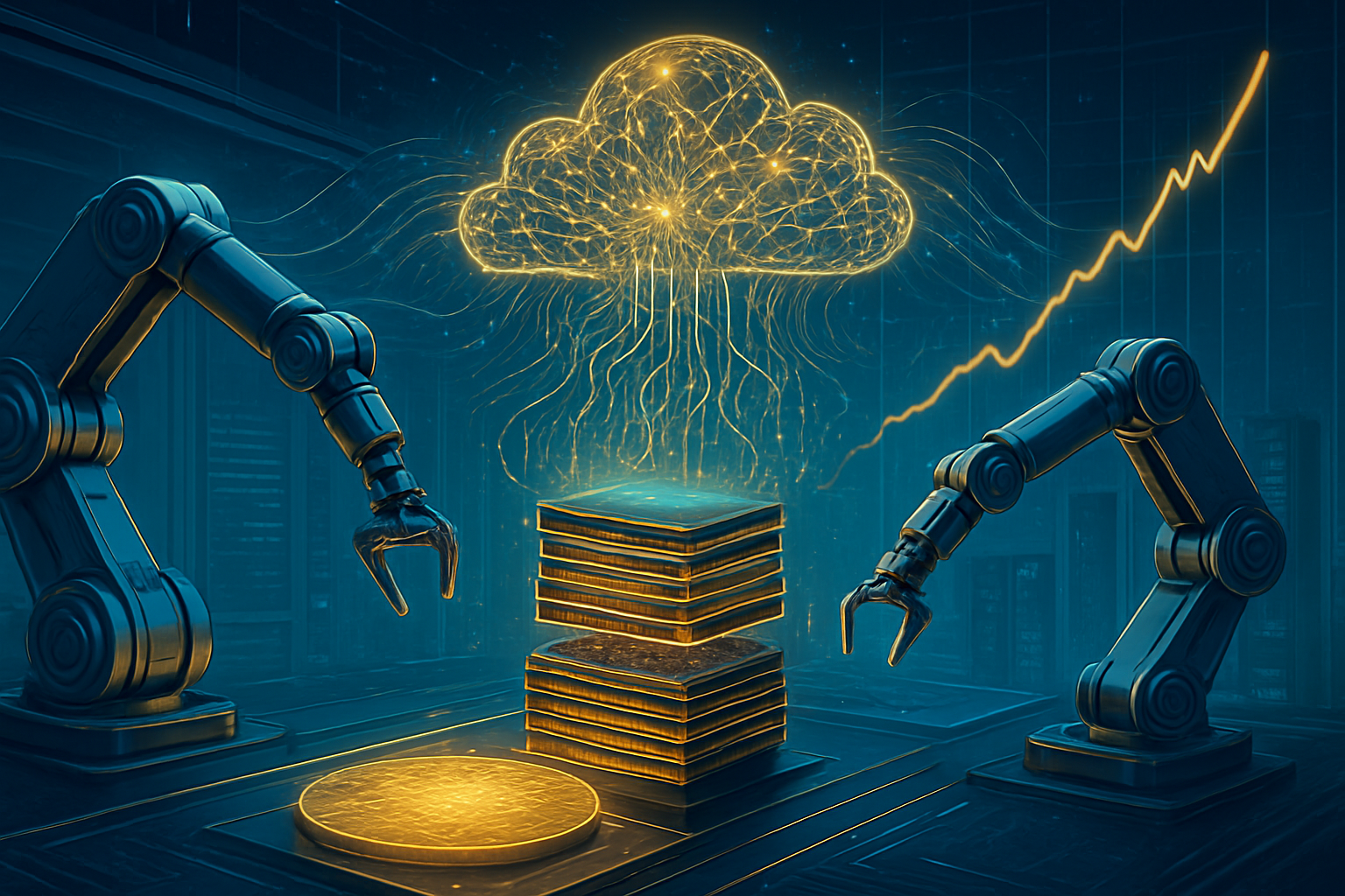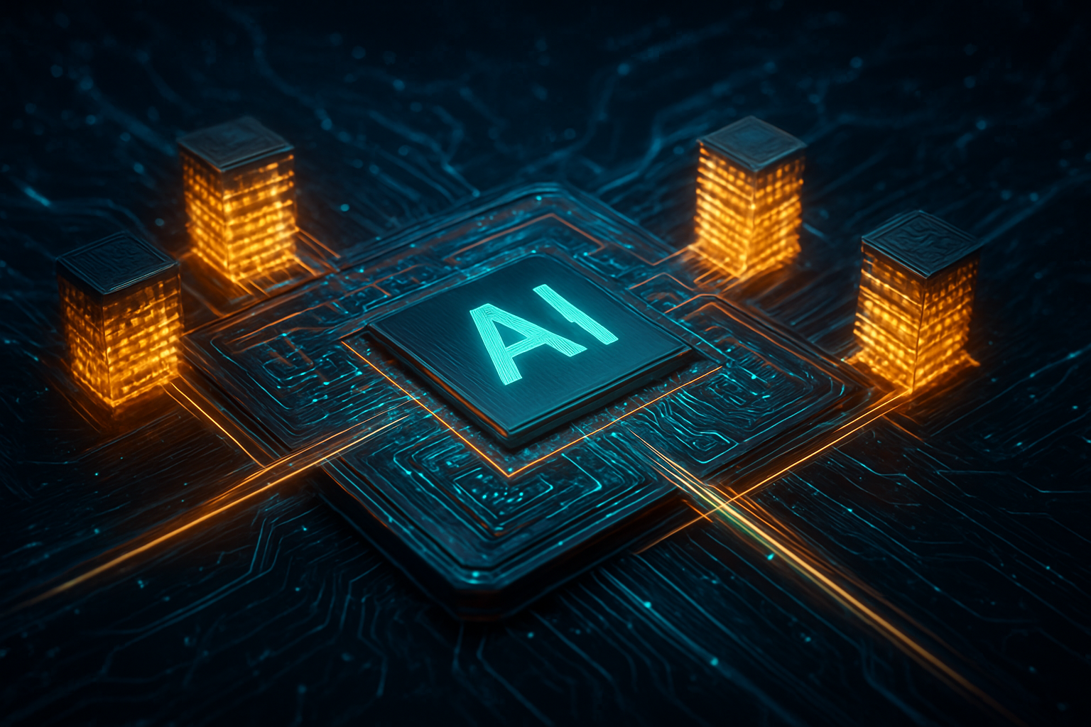
As of January 2026, Tesla (NASDAQ: TSLA) has officially transitioned from a specialized automaker into a "sovereign silicon" powerhouse, solidifying its multi-foundry strategy for the rollout of the AI5 chip. In a move that observers are calling the most aggressive supply chain diversification in the history of the semiconductor industry, Tesla has split its high-volume 2026 production orders between Taiwan Semiconductor Manufacturing Co. (NYSE: TSM) and Samsung Electronics (KRX: 005930). Crucially, this manufacturing is being localized within the United States, utilizing TSMC’s Arizona complex and Samsung’s newly commissioned Taylor, Texas, facility.
The immediate significance of this announcement cannot be overstated. By decoupling its most advanced AI hardware from a single geographic point of failure, Tesla has insulated its future Robotaxi and Optimus humanoid robotics programs from the mounting geopolitical tensions in the Taiwan Strait. This "foundry diversification" not only guarantees a massive volume of chips—essential for the 2026 ramp of the Cybercab—but also grants Tesla unprecedented leverage in the high-end silicon market, setting a new standard for how AI-first companies manage their hardware destiny.
The Architecture of Autonomy: Inside the AI5 Breakthrough
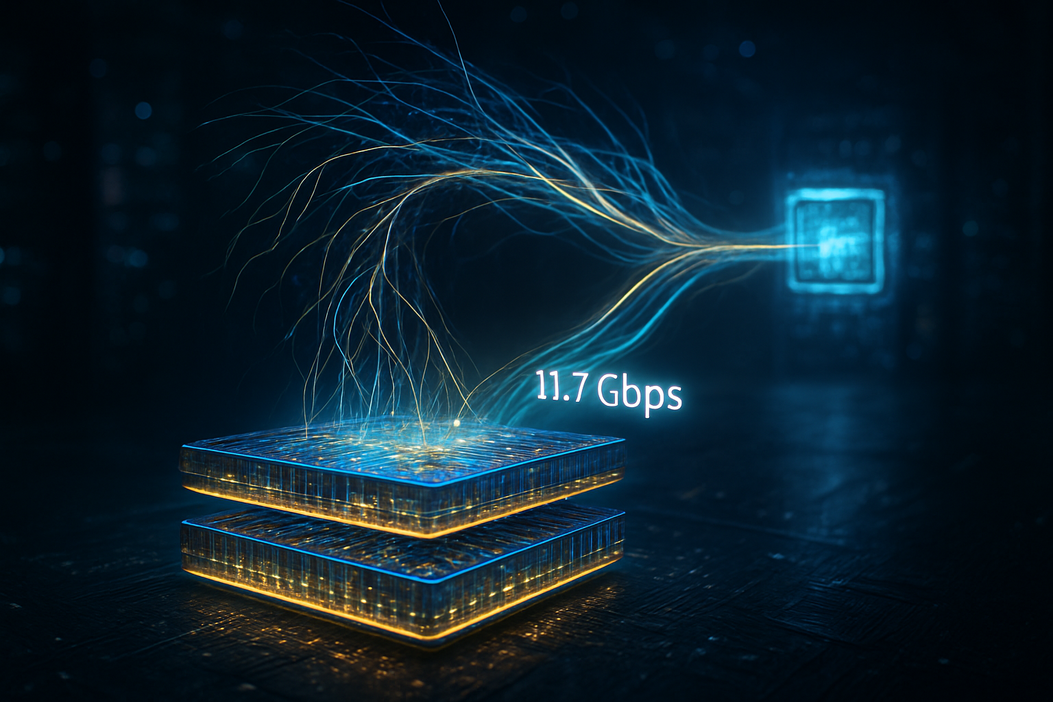
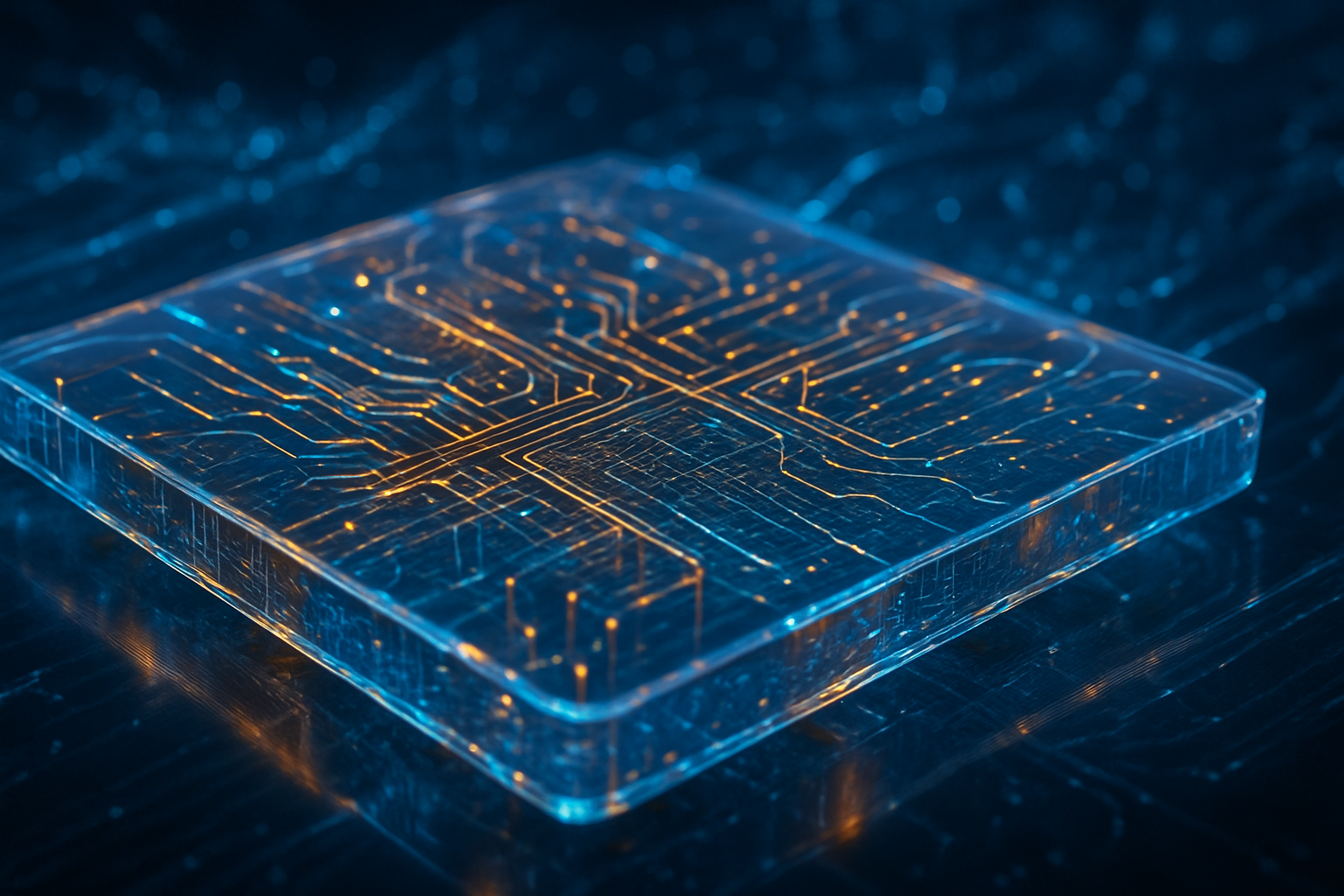
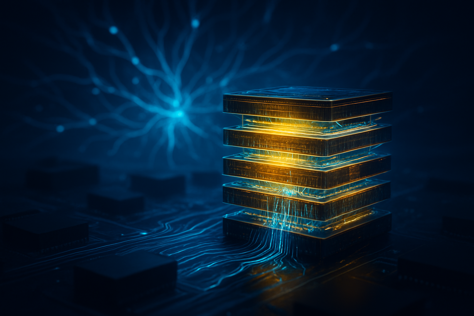
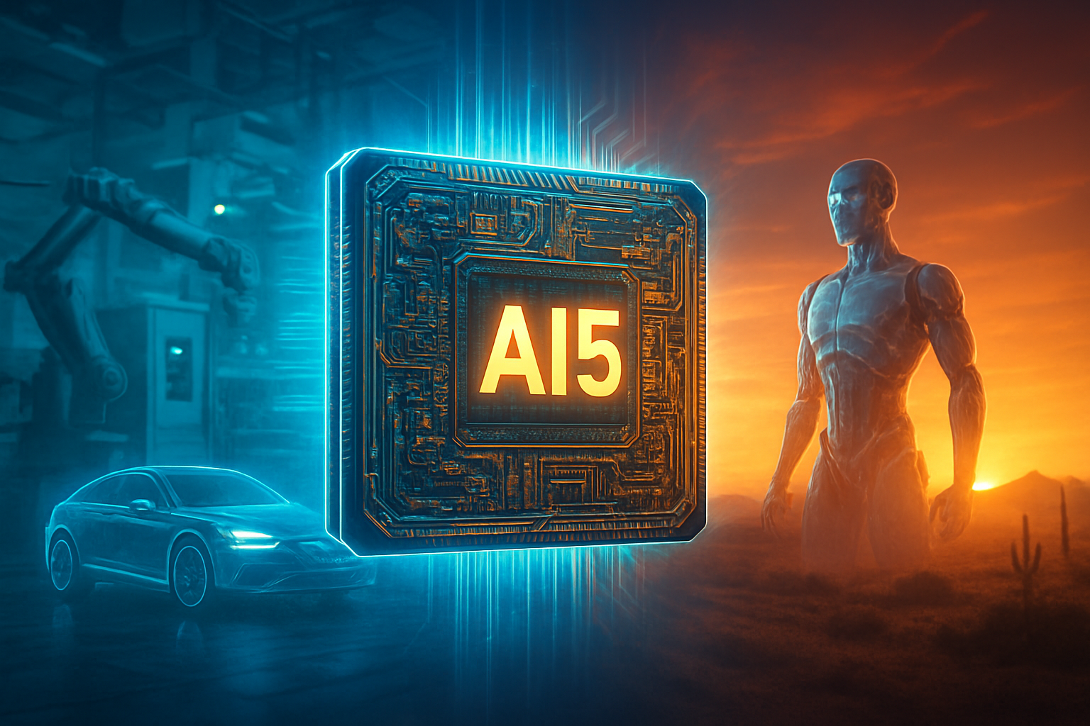
The AI5 silicon, formerly referred to internally as Hardware 5, represents an architectural clean break from its predecessor, Hardware 4 (AI4). While previous generations utilized off-the-shelf blocks for graphics and image processing, AI5 is a "pure AI" system-on-chip (SoC). Tesla engineers have stripped away legacy GPU and Image Signal Processor (ISP) components, dedicating nearly the entire die area to transformer-optimized neural processing units. The result is a staggering leap in performance: AI5 delivers between 2,000 and 2,500 TOPS (Tera Operations Per Second), representing a 4x to 5x increase over the 500 TOPS of HW4.
Manufactured on a mix of 3nm and refined 4nm nodes, AI5 features an integrated memory architecture with bandwidth reaching 1.9 TB/s—nearly five times that of its predecessor. This massive throughput is designed specifically to handle the high-parameter "System 2" reasoning networks required for unsupervised Full Self-Driving (FSD). Initial reactions from the silicon research community highlight Tesla’s shift toward Samsung’s 3nm Gate-All-Around (GAA) architecture at the Taylor fab. Unlike the traditional FinFET structures used by TSMC, Samsung’s GAA process offers superior power efficiency, which is critical for the battery-constrained Optimus Gen 3 humanoid robots.
Industry experts note that this dual-sourcing strategy allows Tesla to play the strengths of both giants against each other. TSMC serves as the primary high-volume "gold standard" for yield reliability in Arizona, while Samsung’s Texas facility provides a cutting-edge playground for the next-generation GAA transistors. By supporting both architectures simultaneously, Tesla has effectively built a software-defined hardware layer that can be compiled for either foundry's specific process, a feat of engineering that few companies outside of Apple (NASDAQ: AAPL) have ever attempted.
Disruption in the Desert: Market Positioning and Competitive Edge
The strategic shift to dual-sourcing creates a significant ripples across the tech ecosystem. For Samsung, the Tesla contract is a vital lifeline that validates its $17 billion investment in Taylor, Texas. Having struggled to capture the top-tier AI business dominated by NVIDIA (NASDAQ: NVDA) and TSMC, Samsung’s ability to secure Tesla’s AI5 and early AI6 prototypes signals a major comeback for the Korean giant in the foundry race. Conversely, while TSMC remains the market leader, Tesla’s willingness to move significant volume to Samsung serves as a warning that even the most "un-fireable" foundry can be challenged if the price and geographic security are right.
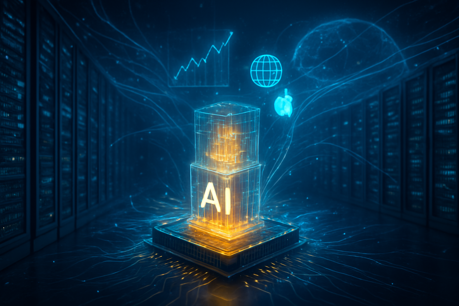
For competitive AI labs and tech giants like Waymo or Amazon (NASDAQ: AMZN), Tesla’s move to "sovereign silicon" creates a daunting barrier to entry. While others rely on general-purpose AI chips from NVIDIA, Tesla’s vertically integrated, purpose-built silicon is tuned specifically for its own software stack. This enables Tesla to run neural networks with 10 times more parameters than current industry standards at a fraction of the power cost. This technical advantage translates directly into market positioning: Tesla can scale its Robotaxi fleet and Optimus deployments with lower per-unit costs and higher computational headroom than any competitor.
Furthermore, the price negotiations stemming from this dual-foundry model have reportedly netted Tesla "sweetheart" pricing from Samsung. Seeking to regain market share, Samsung has offered aggressive terms that allow Tesla to maintain high margins even as it ramps the mass-market Cybercab. This financial flexibility, combined with the security of domestic US production, positions Tesla as a unique entity in the AI landscape—one that controls its AI models, its data, and now, the very factories that print its brains.
Geopolitics and the Rise of Sovereign Silicon
Tesla’s multi-foundry strategy fits into a broader global trend of "Sovereign AI," where companies and nations seek to control their own technological destiny. By localizing production in Texas and Arizona, Tesla is the first major AI player to fully align with the goals of the US CHIPS Act while maintaining a global supply chain footprint. This move mitigates the "Taiwan Risk" that has hung over the semiconductor industry for years. If a supply shock were to occur in the Pacific, Tesla’s US-based lines would remain operational, providing a level of business continuity that its rivals cannot match.
This development marks a milestone in AI history comparable to the first custom-designed silicon for mobile phones. It represents the maturation of the "AI edge" where high-performance computing is no longer confined to the data center but is distributed across millions of mobile robots and vehicles. The shift from "general purpose" to "pure AI" silicon signifies the end of the era where automotive hardware was an afterthought to consumer electronics. In the 2026 landscape, the car and the robot are the primary drivers of semiconductor innovation.
However, the move is not without concerns. Some industry analysts point to the immense complexity of maintaining two separate production lines for the same chip architecture. The risk of "divergent silicon," where chips from Samsung and TSMC perform slightly differently due to process variations, could lead to software optimization headaches. Tesla’s engineering team has countered this by implementing a unified hardware abstraction layer, but the long-term viability of this "parallel development" model will be a major test of the company's technical maturity.
The Horizon: From AI5 to the 9-Month Design Cycle
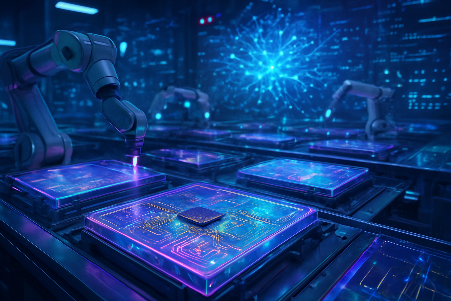
Looking ahead, the AI5 ramp is just the beginning. Reports indicate that Tesla is already moving toward an unprecedented 9-month design cycle for its next generations, AI6 and AI7. By 2027, the goal is for Tesla to refresh its silicon as quickly as AI researchers can iterate on new neural network architectures. This accelerated pace is only possible because the dual-foundry model provides the "hot-swappable" capacity needed to test new designs in one fab while maintaining high-volume production in another.
Potential applications on the horizon go beyond FSD and Optimus. With the massive compute overhead of AI5, Tesla is expected to explore "Dojo-on-the-edge," allowing its vehicles to perform local training of neural networks based on their own unique driving experiences. This would move the AI training loop from the data center directly into the fleet, creating a self-improving system that learns in real-time. Challenges remain, particularly in the scaling of EUV (Extreme Ultraviolet) lithography at the Samsung Taylor plant, but experts predict that once these "teething issues" are resolved by mid-2026, Tesla’s production volume will reach record highs.
Conclusion: A New Era for AI Manufacturing
Tesla’s dual-foundry strategy for AI5 marks a definitive end to the era of single-source dependency in high-end AI silicon. By leveraging the competitive landscape of TSMC and Samsung and anchoring production in the United States, Tesla has secured its path toward global dominance in autonomous transport and humanoid robotics. The AI5 chip is more than just a piece of hardware; it is the physical manifestation of Tesla’s ambition to build the "unified brain" for the physical world.
The key takeaways are clear: vertical integration is no longer enough—geographic and foundry diversification are the new prerequisites for AI leadership at scale. In the coming weeks and months, the tech world will be watching the first yields out of the Samsung Taylor facility and the integration of AI5 into the first production-run Cybercabs. This transition represents a shift in the balance of power in the semiconductor world, proving that for those with the engineering talent to manage it, the "foundry monopoly" is finally over.
This content is intended for informational purposes only and represents analysis of current AI developments.
TokenRing AI delivers enterprise-grade solutions for multi-agent AI workflow orchestration, AI-powered development tools, and seamless remote collaboration platforms.
For more information, visit https://www.tokenring.ai/.