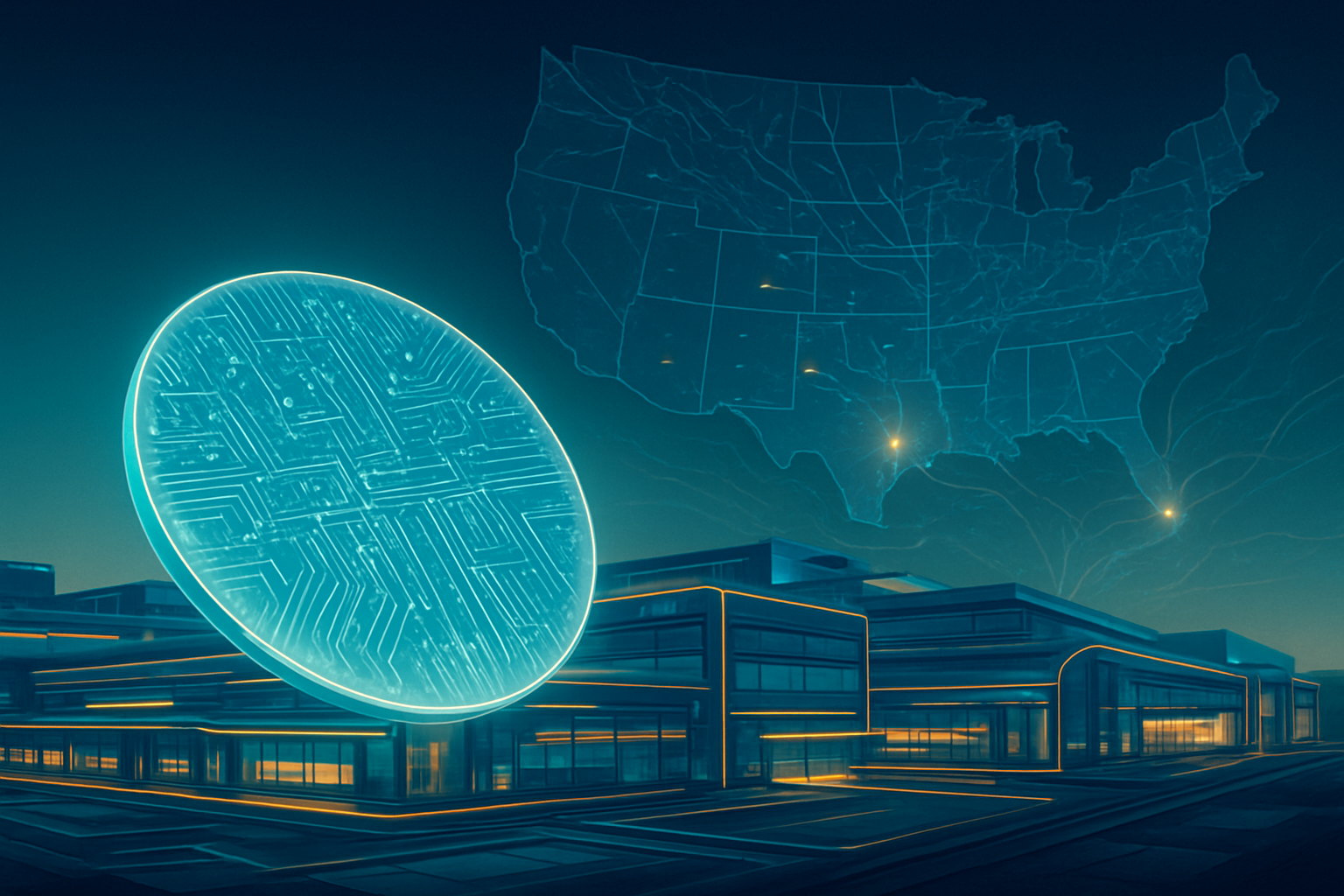
Tag: Samsung

  • Breaking the Silicon Ceiling: How Panel-Level Packaging is Rescuing the AI Revolution from the CoWoS Crunch

    Breaking the Silicon Ceiling: How Panel-Level Packaging is Rescuing the AI Revolution from the CoWoS Crunch

    As of January 2026, the artificial intelligence industry has reached a pivotal infrastructure milestone. For the past three years, the primary bottleneck for the global AI explosion has not been the design of the chips themselves, nor the availability of raw silicon wafers, but rather the specialized "advanced packaging" required to stitch these complex processors together. TSMC (NYSE: TSM) has spent the last 24 months in a frantic race to expand its Chip-on-Wafer-on-Substrate (CoWoS) capacity, which is projected to reach an staggering 125,000 wafers per month by the end of this year—a nearly four-fold increase from early 2024 levels.

    Despite this massive scale-up, the insatiable demand from hyperscalers and AI chip giants like Nvidia (NASDAQ: NVDA) and AMD (NASDAQ: AMD) has kept the capacity effectively "sold out" through 2026. This persistent supply-demand imbalance has forced a paradigm shift in semiconductor manufacturing. The industry is now rapidly transitioning from traditional circular 300mm silicon wafers to a revolutionary new format: Panel-Level Packaging (PLP). This shift, spearheaded by new technological deployments like TSMC’s CoPoS and Intel’s commercial glass substrates, represents the most significant change to chip assembly in decades, promising to break the "reticle limit" and usher in an era of massive, multi-chiplet super-processors.

    Scaling Beyond the Circle: The Technical Leap to Panels

    The technical limitation of current advanced packaging lies in the geometry of the wafer. Since the late 1990s, the industry standard has been the 300mm (12-inch) circular silicon wafer. However, as AI chips like Nvidia’s Blackwell and the newly announced Rubin architectures grow larger and require more High Bandwidth Memory (HBM) stacks, they are reaching the physical limits of what a circular wafer can efficiently accommodate. Panel-Level Packaging (PLP) solves this by moving from circular wafers to large rectangular panels, typically starting at 310mm x 310mm and scaling up to a massive 600mm x 600mm.

    TSMC’s entry into this space, branded as CoPoS (Chip-on-Panel-on-Substrate), represents an evolution of its CoWoS technology. By using rectangular panels, manufacturers can achieve area utilization rates of over 95%, compared to the roughly 80% efficiency of circular wafers, where the edges often result in "scrap" silicon. Furthermore, the transition to glass substrates—a breakthrough Intel (NASDAQ: INTC) moved into High-Volume Manufacturing (HVM) this month—is replacing traditional organic materials. Glass offers 50% less pattern distortion and superior thermal stability, allowing for the extreme interconnect density required for the 1,000-watt AI chips currently entering the market.

    Initial reactions from the AI research community have been overwhelmingly positive, as these innovations allow for "super-packages" that were previously impossible. Experts at the 2026 International Solid-State Circuits Conference (ISSCC) noted that PLP and glass substrates are the only viable path to integrating HBM4 memory, which requires twice the interconnect density of its predecessors. This transition essentially allows chipmakers to treat the packaging itself as a giant, multi-layered circuit board, effectively extending the lifespan of Moore’s Law through physical assembly rather than transistor shrinking alone.

    The Competitive Scramble: Market Leaders and the OSAT Alliance

    The shift to PLP has reshuffled the competitive landscape of the semiconductor industry. While TSMC remains the dominant player, securing over 60% of Nvidia's packaging orders for the next two years, the bottleneck has opened a window of opportunity for rivals. Intel has leveraged its first-mover advantage in glass substrates to position its 18A foundry services as a high-end alternative for companies seeking to avoid the TSMC backlog. Intel’s Chandler, Arizona facility is now fully operational, providing a "turnkey" advanced packaging solution on U.S. soil—a strategic advantage that has already attracted attention from defense and aerospace sectors.

    Samsung (KRX: 005930) is also mounting a significant challenge through its "Triple Alliance" strategy, which integrates its display technology, electro-mechanics, and chip manufacturing arms. Samsung’s I-CubeE (Fan-Out Panel-Level Packaging) is currently being deployed to help customers like Broadcom (NASDAQ: AVGO) reduce costs by replacing expensive silicon interposers with embedded silicon bridges. This has allowed Samsung to capture a larger share of the "value-tier" AI accelerator market, providing a release valve for the high-end CoWoS shortage.

    Outsourced Semiconductor Assembly and Test (OSAT) providers are also benefiting from this shift. TSMC has increasingly outsourced the "back-end" portions of the process (the "on-Substrate" part of CoWoS) to partners like ASE Technology (NYSE: ASX) and Amkor (NASDAQ: AMKR). By 2026, ASE is expected to handle nearly 45% of the back-end packaging for TSMC’s customers. This ecosystem approach has allowed the industry to scale output more rapidly than any single company could achieve alone, though it has also led to a 10-20% increase in packaging prices due to the sheer complexity of the multi-vendor supply chain.

    The "Packaging Era" and the Future of AI Economics

    The broader significance of the PLP transition cannot be overstated. We have moved from the "Lithography Era," where the most important factor was the size of the transistor, to the "Packaging Era," where the most important factor is the speed and density of the connection between chiplets. This shift is fundamentally changing the economics of AI. Because advanced packaging is so capital-intensive, the barrier to entry for creating high-end AI chips has skyrocketed. Only a handful of companies can afford the multi-billion dollar "entry fee" required to secure CoWoS or PLP capacity at scale.

    However, there are growing concerns regarding the environmental and yield-related costs of this transition. Moving to 600mm panels requires entirely new sets of factory tools, and the early yield rates for PLP are significantly lower than those for mature 300mm wafer processes. Critics also point out that the centralization of advanced packaging in Taiwan remains a geopolitical risk, although the expansion of TSMC and Amkor into Arizona is a step toward diversification. The "warpage wall"—the tendency for large panels to bend under intense heat—remains a major engineering hurdle that companies are only now beginning to solve through the use of glass cores.

    What’s Next: The Road to 2028 and the "1 Trillion Transistor" Chip

    Looking ahead, the next two years will be defined by the transition from pilot lines to high-volume manufacturing for panel-level technologies. TSMC has scheduled the mass production of its CoPoS technology for late 2027 or early 2028, coinciding with the expected launch of "Post-Rubin" AI architectures. These future chips are predicted to feature "all-glass" substrates and integrated silicon photonics, allowing for light-speed data transfer between the processor and memory.

    The ultimate goal, as articulated by Intel and TSMC leaders, is the "1 Trillion Transistor System-in-Package" by 2030. Achieving this will require panels even larger than today's prototypes and a complete overhaul of how we manage heat in data centers. We should expect to see a surge in "co-packaged optics" announcements in late 2026, as the electrical limits of traditional substrates finally give way to optical interconnects. The primary challenge remains yield; as chips grow larger, the probability of a single defect ruining a multi-thousand-dollar package increases exponentially.

    A New Foundation for Artificial Intelligence

    The resolution of the CoWoS bottleneck through the adoption of Panel-Level Packaging and glass substrates marks a definitive turning point in the history of computing. By breaking the geometric constraints of the 300mm wafer, the industry has paved the way for a new generation of AI hardware that is exponentially more powerful than the chips that fueled the initial 2023-2024 AI boom.

    As we move through the first half of 2026, the key indicators of success will be the yield rates of Intel's glass substrate lines and the speed at which TSMC can bring its Chiayi AP7 facility to full capacity. While the shortage of AI compute has eased slightly due to these massive investments, the "structural demand" for intelligence suggests that packaging will remain a high-stakes battlefield for the foreseeable future. The silicon ceiling hasn't just been raised; it has been replaced by a new, rectangular, glass-bottomed foundation.


    This content is intended for informational purposes only and represents analysis of current AI developments.

    TokenRing AI delivers enterprise-grade solutions for multi-agent AI workflow orchestration, AI-powered development tools, and seamless remote collaboration platforms.
    For more information, visit https://www.tokenring.ai/.

  • The High-NA Revolution: Inside the $400 Million Machines Defining the Angstrom Era

    The High-NA Revolution: Inside the $400 Million Machines Defining the Angstrom Era

    The global race for artificial intelligence supremacy has officially entered its most expensive and physically demanding chapter yet. As of early 2026, the transition from experimental R&D to high-volume manufacturing (HVM) for High-Numerical Aperture (High-NA) Extreme Ultraviolet (EUV) lithography is complete. These massive, $400 million machines, manufactured exclusively by ASML (NASDAQ: ASML), have become the literal gatekeepers of the "Angstrom Era," enabling the production of transistors so small that they are measured by the width of individual atoms.

    The arrival of High-NA EUV is not merely an incremental upgrade; it is a critical pivot point for the entire AI industry. As Large Language Models (LLMs) scale toward 100-trillion parameter architectures, the demand for more energy-efficient and dense silicon has made traditional lithography obsolete. Without the precision afforded by High-NA, the hardware required to sustain the current pace of AI development would hit a "thermal wall," where energy consumption and heat dissipation would outpace any gains in raw processing power.

    The Optical Engineering Marvel: 0.55 NA and the End of Multi-Patterning

    At the heart of this revolution is the ASML Twinscan EXE:5200 series. The "High-NA" designation refers to the increase in numerical aperture from 0.33 to 0.55. In the world of optics, a higher NA allows the lens system to collect more light and achieve a finer resolution. For chipmakers, this means the ability to print features as small as 8nm, a significant leap from the 13nm limit of previous-generation EUV tools. This increased resolution enables a nearly 3-fold increase in transistor density, allowing engineers to cram more logic and memory into the same square millimeter of silicon.

    The most immediate technical benefit for foundries is the return to "single-patterning." In the previous sub-3nm era, manufacturers were forced to use complex "multi-patterning" techniques—essentially printing a single layer of a chip across multiple exposures—to bypass the resolution limits of 0.33 NA machines. This process was notoriously error-prone, time-consuming, and decimated yields. The High-NA systems allow for these intricate designs to be printed in a single pass, slashing the number of critical layer process steps from over 40 to fewer than 10. This efficiency is what makes the 1.4nm (Intel 14A) and upcoming 1nm nodes economically viable.

    Initial reactions from the semiconductor research community have been a mix of awe and cautious pragmatism. While the technical capabilities of the EXE:5200B are undisputed—boasting a throughput of over 200 wafers per hour and sub-nanometer overlay accuracy—the sheer scale of the hardware has presented logistical nightmares. These machines are roughly the size of a double-decker bus and weigh 150,000 kilograms, requiring cleanrooms with reinforced flooring and specialized ceiling heights that many older fabs simply cannot accommodate.

    The Competitive Tectonic Shift: Intel’s Lead and the Foundries' Dilemma

    The deployment of High-NA has created a stark strategic divide among the world’s leading chipmakers. Intel (NASDAQ: INTC) has emerged as the early winner in this transition, having successfully completed acceptance testing for its first high-volume EXE:5200B system in Oregon this month. By being the "First Mover," Intel is leveraging High-NA to underpin its Intel 14A node, aiming to reclaim the title of process leadership from its rivals. This aggressive stance is a cornerstone of Intel Foundry's strategy to attract external customers like NVIDIA (NASDAQ: NVDA) and Microsoft (NASDAQ: MSFT) who are desperate for the most advanced AI silicon.

    In contrast, TSMC (NYSE: TSM) has adopted a "calculated delay" strategy. The Taiwanese giant has spent the last year optimizing its A16 (1.6nm) node using older 0.33 NA machines with sophisticated multi-patterning to maintain its industry-leading yields. However, TSMC is not ignoring the future; the company has reportedly secured an massive order of nearly 70 High-NA machines for its A14 and A10 nodes slated for 2027 and beyond. This creates a fascinating competitive window where Intel may have a technical density advantage, while TSMC maintains a volume and cost-efficiency lead.

    Meanwhile, Samsung (KRX: 005930) is attempting a high-stakes "leapfrog" maneuver. After integrating its first High-NA units for 2nm production, internal reports suggest the company may skip the 1.4nm node entirely to focus on a "dream" 1nm process. This strategic pivot is intended to close the gap with TSMC by betting on the ultimate physical limit of silicon earlier than its competitors. For AI labs and chip designers, this means the next three years will be defined by which foundry can most effectively balance the astronomical costs of High-NA with the performance demands of next-gen Blackwell and Rubin-class GPUs.

    Moore's Law and the "2-Atom Wall"

    The wider significance of High-NA EUV lies in its role as the ultimate life-support system for Moore’s Law. We are no longer just fighting the laws of economics; we are fighting the laws of physics. At the 1.4nm and 1nm levels, we are approaching what researchers call the "2-atom wall"—a point where transistor features are only two atoms thick. Beyond this, traditional silicon faces insurmountable challenges from quantum tunneling, where electrons literally jump through barriers they are supposed to be blocked by, leading to massive data errors and power leakage.

    High-NA is being used in tandem with other radical architectures to circumvent these limits. Technologies like Backside Power Delivery (which Intel calls PowerVia) move the power lines to the back of the wafer, freeing up space on the front for even denser transistor placement. This synergy is what allows for the power-efficiency gains required for the next generation of "Physical AI"—autonomous robots and edge devices that need massive compute power without being tethered to a power plant.

    However, the concentration of this technology in the hands of a single supplier, ASML, and three primary customers raises significant concerns about the democratization of AI. The $400 million price tag per machine, combined with the billions required for fab construction, creates a barrier to entry that effectively locks out any new players in the leading-edge foundry space. This consolidation ensures that the "AI haves" and "AI have-nots" will be determined by who has the deepest pockets and the most stable supply chains for Dutch-made optics.

    The Horizon: Hyper-NA and the Sub-1nm Future

    As the industry digests the arrival of High-NA, ASML is already looking toward the next frontier: Hyper-NA. With a projected numerical aperture of 0.75, Hyper-NA systems (likely the HXE series) are already on the roadmap for 2030. These machines will be necessary to push manufacturing into the sub-10-Angstrom (sub-1nm) range. However, experts predict that Hyper-NA will face even steeper challenges, including "polarization death," where the angles of light become so extreme that they cancel each other out, requiring entirely new types of polarization filters.

    In the near term, the focus will shift from "can we print it?" to "can we yield it?" The industry is expected to see a surge in the use of AI-driven metrology and inspection tools to manage the extreme precision required by High-NA. We will also likely see a major shift in material science, with researchers exploring 2D materials like molybdenum disulfide to replace silicon as we hit the 2-atom wall. The chips powering the AI models of 2028 and beyond will likely look nothing like the processors we use today.

    Conclusion: A Tectonic Moment in Computing History

    The successful deployment of ASML’s High-NA EUV tools marks one of the most significant milestones in the history of the semiconductor industry. It represents the pinnacle of human engineering—using light to manipulate matter at the near-atomic scale. For the AI industry, this is the infrastructure that makes the "Sovereign AI" dreams of nations and the "AGI" goals of labs possible.

    The key takeaways for the coming year are clear: Intel has secured a narrow but vital head start in the Angstrom era, while TSMC remains the formidable incumbent betting on refined execution. The massive capital expenditure required for these tools will likely drive up the price of high-end AI chips, but the performance and efficiency gains will be the engine that drives the next decade of digital transformation. Watch closely for the first 1.4nm "tape-outs" from major AI players in the second half of 2026; they will be the first true test of whether the $400 million gamble has paid off.


    This content is intended for informational purposes only and represents analysis of current AI developments.

    TokenRing AI delivers enterprise-grade solutions for multi-agent AI workflow orchestration, AI-powered development tools, and seamless remote collaboration platforms.
    For more information, visit https://www.tokenring.ai/.

  • The GAA Era Arrives: TSMC Enters Mass Production of 2nm Chips to Fuel the Next AI Supercycle

    The GAA Era Arrives: TSMC Enters Mass Production of 2nm Chips to Fuel the Next AI Supercycle

    As the calendar turns to early 2026, the global semiconductor landscape has officially shifted on its axis. Taiwan Semiconductor Manufacturing Company (NYSE:TSM), commonly known as TSMC, has successfully crossed the finish line of its most ambitious technological transition in a decade. Following a rigorous ramp-up period that concluded in late 2025, the company’s 2nm (N2) node is now in high-volume manufacturing, ushering in the era of Gate-All-Around (GAA) nanosheet transistors. This milestone marks more than just a reduction in feature size; it represents the foundational infrastructure upon which the next generation of generative AI and high-performance computing (HPC) will be built.

    The immediate significance of this development cannot be overstated. By moving into volume production ahead of its most optimistic competitors and maintaining superior yield rates, TSMC has effectively secured its position as the primary engine of the AI economy. With primary production hubs at Fab 22 in Kaohsiung and Fab 20 in Hsinchu reaching a combined output of over 50,000 wafers per month this January, the company is already churning out the silicon that will power the most advanced smartphones and data center accelerators of 2026 and 2027.

    The Nanosheet Revolution: Engineering the Future of Silicon

    The N2 node represents a fundamental departure from the FinFET (Fin Field-Effect Transistor) architecture that has dominated the industry for the last several process generations. In traditional FinFETs, the gate controls the channel on three sides; however, as transistors shrink toward the 2nm threshold, current leakage becomes an insurmountable hurdle. TSMC’s shift to Gate-All-Around (GAA) nanosheet transistors solves this by wrapping the gate around all four sides of the channel, providing superior electrostatic control and drastically reducing power leakage.

    Technical specifications for the N2 node are staggering. Compared to the previous 3nm (N3E) process, the 2nm node offers a 10% to 15% increase in performance at the same power envelope, or a significant 25% to 30% reduction in power consumption at the same clock speed. Furthermore, the N2 node introduces "Super High-Performance Metal-Insulator-Metal" (SHPMIM) capacitors. These components double the capacitance density while cutting resistance by 50%, a critical advancement for AI chips that must handle massive, instantaneous power draws without losing efficiency. Early logic test chips have reportedly achieved yield rates between 70% and 80%, a metric that validates TSMC's manufacturing prowess compared to the more volatile early yields seen in rival GAA implementations.

    A High-Stakes Duel: Intel, Samsung, and the Battle for Foundry Supremacy

    The successful ramp of N2 has profound implications for the competitive balance between the "Big Three" chipmakers. While Samsung Electronics (KRX:005930) was technically the first to move to GAA at the 3nm stage, its yields have historically struggled to compete with the stability of TSMC. Samsung’s recent launch of the SF2 node and the Exynos 2600 chip shows progress, but the company remains primarily a secondary source for major designers. Meanwhile, Intel (NASDAQ:INTC) has emerged as a formidable challenger with its 18A node. Intel’s 18A utilizes "PowerVia" (Backside Power Delivery), a technology TSMC will not integrate until its N2P variant in late 2026. This gives Intel a temporary technical lead in raw power delivery metrics, even as TSMC maintains a superior transistor density of roughly 313 million transistors per square millimeter.

    For the world’s most valuable tech giants, the arrival of N2 is a strategic windfall. Apple (NASDAQ:AAPL), acting as TSMC’s "alpha" customer, has reportedly secured over 50% of the initial 2nm capacity to power its upcoming iPhone 18 series and the M5/M6 Mac silicon. Close on their heels is Nvidia (NASDAQ:NVDA), which is leveraging the N2 node for its next-generation AI platforms succeeding the Blackwell architecture. Other major players including Advanced Micro Devices (NASDAQ:AMD), Broadcom (NASDAQ:AVGO), and MediaTek (TPE:2454) have already finalized their 2026 production slots, signaling a collective industry bet that TSMC’s N2 will be the gold standard for efficiency and scale.

    Scaling AI: The Broader Landscape of 2nm Integration

    The transition to 2nm is inextricably linked to the trajectory of artificial intelligence. As Large Language Models (LLMs) grow in complexity, the demand for "compute" has become the defining constraint of the tech industry. The 25-30% power savings offered by N2 are not merely a luxury for mobile devices; they are a survival necessity for data centers. By reducing the energy required per inference or training cycle, 2nm chips allow hyperscalers like Microsoft (NASDAQ:MSFT) and Amazon (NASDAQ:AMZN) to pack more density into their existing power footprints, potentially slowing the skyrocketing environmental costs of the AI boom.

    This milestone also reinforces the "Moore's Law is not dead" narrative, albeit with a caveat: while transistor density continues to increase, the cost per transistor is rising. The complexity of GAA manufacturing requires multi-billion dollar investments in Extreme Ultraviolet (EUV) lithography and specialized cleanrooms. This creates a widening "innovation gap" where only the largest, most capitalized companies can afford the leap to 2nm, potentially consolidating power within a handful of AI leaders while leaving smaller startups to rely on older, less efficient silicon.

    The Roadmap Beyond: A16 and the 1.6nm Frontier

    The arrival of 2nm mass production is just the beginning of a rapid-fire roadmap. TSMC has already disclosed that its N2P node—the enhanced version of 2nm featuring Backside Power Delivery—is on track for mass production in late 2026. This will be followed closely by the A16 node (1.6nm) in 2027, which will incorporate "Super PowerRail" technology to further optimize power distribution directly to the transistor's source and drain.

    Experts predict that the next eighteen months will focus on "advanced packaging" as much as the nodes themselves. Technologies like CoWoS (Chip on Wafer on Substrate) will be essential to combine 2nm logic with high-bandwidth memory (HBM4) to create the massive AI "super-chips" of the future. The challenge moving forward will be heat dissipation; as transistors become more densely packed, managing the thermal output of these 2nm dies will require innovative liquid cooling and material science breakthroughs.

    Conclusion: A Pivot Point for the Digital Age

    TSMC’s successful transition to the 2nm N2 node in early 2026 stands as one of the most significant engineering feats of the decade. By navigating the transition from FinFET to GAA nanosheets while maintaining industry-leading yields, the company has solidified its role as the indispensable foundation of the AI era. While Intel and Samsung continue to provide meaningful competition, TSMC’s ability to scale this technology for giants like Apple and Nvidia ensures that the heartbeat of global innovation remains centered in Taiwan.

    In the coming months, the industry will watch closely as the first 2nm consumer devices hit the shelves and the first N2-based AI clusters go online. This development is more than a technical upgrade; it is the starting gun for a new epoch of computing performance, one that will determine the pace of AI advancement for years to come.


    This content is intended for informational purposes only and represents analysis of current AI developments.

    TokenRing AI delivers enterprise-grade solutions for multi-agent AI workflow orchestration, AI-powered development tools, and seamless remote collaboration platforms.
    For more information, visit https://www.tokenring.ai/.

  • The Silicon Sustainability Crisis: Inside the Multi-Billion Dollar Push for ‘Green Fabs’ in 2026

    The Silicon Sustainability Crisis: Inside the Multi-Billion Dollar Push for ‘Green Fabs’ in 2026

    As of January 2026, the artificial intelligence revolution has reached a critical paradox. While AI is being hailed as the ultimate tool to solve the climate crisis, the physical infrastructure required to build it—massive semiconductor manufacturing plants known as "mega-fabs"—has become one of the world's most significant environmental challenges. The explosive demand for next-generation AI chips from companies like NVIDIA (NASDAQ:NVDA) is forcing the world’s three largest chipmakers to fundamentally redesign the "factory of the future."

    Intel (NASDAQ:INTC), TSMC (NYSE:TSM), and Samsung (KRX:005930) are currently locked in a high-stakes race to build "Green Fabs." These multi-billion dollar facilities, located from the deserts of Arizona to the plains of Ohio and the industrial hubs of South Korea, are no longer just measured by their nanometer precision. In 2026, the primary metrics for success have shifted to "Net-Zero Liquid Discharge" and "24/7 Carbon-Free Energy." This shift marks a historic turning point where environmental sustainability is no longer a corporate social responsibility (CSR) footnote but a core requirement for high-volume manufacturing.

    The Technical Toll of 2nm: Powering the High-NA EUV Era

    The push for Green Fabs is driven by the extreme technical requirements of the latest chip nodes. To produce the 2nm and sub-2nm chips required for 2026-era AI models, manufacturers must use High-NA (Numerical Aperture) Extreme Ultraviolet (EUV) lithography machines produced by ASML (NASDAQ:ASML). These machines are engineering marvels but energy gluttons; a single High-NA EUV unit (such as the EXE:5200) consumes approximately 1.4 megawatts of electricity—enough to power over a thousand homes. When a single mega-fab houses dozens of these machines, the power demand rivals that of a mid-sized city.

    To mitigate this, the "Big Three" are deploying radical new efficiency technologies. Samsung recently announced a partnership with NVIDIA to deploy "Autonomous Digital Twins" across its Taylor, Texas facility. This system uses tens of thousands of sensors and AI-driven simulations to optimize airflow and chemical delivery in real-time, reportedly improving energy efficiency by 20% compared to 2024 standards. Meanwhile, Intel is experimenting with hydrogen recovery systems in its upcoming Magdeburg, Germany site, capturing and reusing the hydrogen gas used during the lithography process to generate supplemental on-site power.

    Water scarcity has become the second technical hurdle. In Arizona, TSMC has pioneered a 15-acre Industrial Water Reclamation Plant (IWRP) that aims for a 90% recycling rate. This "closed-loop" system ensures that nearly every gallon of water used to wash silicon wafers is treated and returned to the cleanroom, leaving only evaporation as a source of loss. This is a massive leap from a decade ago, when semiconductor manufacturing was notorious for depleting local aquifers and discharging chemical-heavy wastewater.

    The Nuclear Renaissance and the Power Struggle for the Grid

    The sheer scale of energy required for AI chip production has sparked a "nuclear renaissance" in the semiconductor industry. In late 2025, Samsung C&T signed landmark agreements with Small Modular Reactor (SMR) pioneers like NuScale and X-energy. By early 2026, the strategy is clear: because solar and wind cannot provide the 24/7 "baseload" power required for a fab that never sleeps, chipmakers are turning to dedicated nuclear solutions. This move is supported by tech giants like Microsoft (NASDAQ:MSFT) and Amazon (NASDAQ:AMZN), who have recently secured nearly 6 gigawatts of nuclear power to ensure the fabs and data centers they rely on remain carbon-neutral.

    However, this hunger for power has led to unprecedented corporate friction. In a notable incident in late 2025, Meta (NASDAQ:META) reportedly petitioned Ohio regulators to reassign 200 megawatts of power capacity originally reserved for Intel’s New Albany mega-fab. Meta argued that because Intel’s high-volume production had been delayed to 2030, the power would be better used for Meta’s nearby AI data centers. This "power grab" highlights a growing tension: as the world transitions to green energy, the supply of stable, renewable power is becoming a more significant bottleneck than silicon itself.

    For startups and smaller AI labs, the emergence of Green Fabs creates a two-tiered market. Companies that can afford to pay the premium for "Green Silicon" will see their ESG (Environmental, Social, and Governance) scores soar, making them more attractive to institutional investors. Conversely, those relying on older, "dirtier" fabs may find themselves locked out of certain markets or facing carbon taxes that erode their margins.

    Environmental Justice and the Global Landscape

    The transition to Green Fabs is also a response to growing geopolitical and social pressure. In Taiwan, TSMC has faced recurring droughts that threatened both chip production and local agriculture. By investing in 100% renewable energy and advanced water recycling, TSMC is not just being "green"—it is ensuring its survival in a region where resources are increasingly contested. Similarly, Intel’s "Net-Positive Water" goal for its Ohio site involves funding massive wetland restoration projects, such as the Dillon Lake initiative, to balance its environmental footprint.

    Critics, however, point to a "structural sustainability risk" in the way AI chips are currently made. The demand for High-Bandwidth Memory (HBM), essential for AI GPUs, has led to a "stacking loss" crisis. In early 2026, the complexity of 16-high HBM stacks has resulted in lower yields, meaning a significant amount of silicon and energy is wasted on defective chips. Industry experts argue that until yields improve, the "greenness" of a fab is partially offset by the waste generated in the pursuit of extreme performance.

    This development fits into a broader trend where the "hidden costs" of AI are finally being accounted for. Much like the transition from coal to renewables in the 2010s, the semiconductor industry is realizing that the old model of "performance at any cost" is no longer viable. The Green Fab movement is the hardware equivalent of the "Efficient AI" software trend, where researchers are moving away from massive, "brute-force" models toward more optimized, energy-efficient architectures.

    Future Horizons: 1.4nm and Beyond

    Looking ahead to the late 2020s, the industry is already eyeing the 1.4nm node, which will require even more specialized equipment and even greater power density. Experts predict that the next generation of fabs will be built with integrated SMRs directly on-site, effectively making them "energy islands" that do not strain the public grid. We are also seeing the emergence of "Circular Silicon" initiatives, where the rare earth metals and chemicals used in fab processes are recovered with near 100% efficiency.

    The challenge remains the speed of infrastructure. While software can be updated in seconds, a mega-fab takes years to build and decades to pay off. The "Green Fabs" of 2026 are the first generation of facilities designed from the ground up for a carbon-constrained world, but the transition of older "legacy" fabs remains a daunting task. Analysts expect that by 2028, the "Green Silicon" certification will become a standard industry requirement, much like "Organic" or "Fair Trade" labels in other sectors.

    Summary of the Green Revolution

    The push for Green Fabs in 2026 represents one of the most significant industrial shifts in modern history. Intel, TSMC, and Samsung are no longer just competing on the speed of their transistors; they are competing on the sustainability of their supply chains. The integration of SMRs, AI-driven digital twins, and closed-loop water systems has transformed the semiconductor fab from an environmental liability into a model of high-tech conservation.

    As we move through 2026, the success of these initiatives will determine the long-term viability of the AI boom. If the industry can successfully decouple computing growth from environmental degradation, the promise of AI as a tool for global good will remain intact. For now, the world is watching the construction cranes in Ohio, Arizona, and Texas, waiting to see if the silicon of tomorrow can truly be green.


    This content is intended for informational purposes only and represents analysis of current AI developments.

    TokenRing AI delivers enterprise-grade solutions for multi-agent AI workflow orchestration, AI-powered development tools, and seamless remote collaboration platforms.
    For more information, visit https://www.tokenring.ai/.

  • The Nanosheet Revolution: Why GAAFET at 2nm is the New ‘Thermal Wall’ Solution for AI

    The Nanosheet Revolution: Why GAAFET at 2nm is the New ‘Thermal Wall’ Solution for AI

    As of January 2026, the semiconductor industry has reached its most significant architectural milestone in over a decade: the transition from the FinFET (Fin Field-Effect Transistor) to the Gate-All-Around (GAAFET) nanosheet architecture. This shift, led by industry titans TSMC (NYSE: TSM), Samsung (KRX: 005930), and Intel (NASDAQ: INTC), marks the end of the "fin" era that dominated chip manufacturing since the 22nm node. The transition is not merely a matter of incremental scaling; it is a fundamental survival tactic for the artificial intelligence industry, which has been rapidly approaching a "thermal wall" where power leakage threatened to stall the development of next-generation GPUs and AI accelerators.

    The immediate significance of the 2nm GAAFET transition lies in its ability to sustain the exponential growth of Large Language Models (LLMs) and generative AI. With data center power envelopes now routinely exceeding 1,000 watts per rack unit, the industry required a transistor that could deliver higher performance without a proportional increase in heat. By surrounding the conducting channel on all four sides with the gate, GAAFETs provide the electrostatic control necessary to eliminate the "short-channel effects" that plagued FinFETs at the 3nm boundary. This development ensures that the hardware roadmap for AI—driven by massive compute demands—can continue through the end of the decade.

    Engineering the 360-Degree Gate: The End of FinFET

    The technical necessity for GAAFET stems from the physical limitations of the FinFET structure. In a FinFET, the gate wraps around three sides of a vertical "fin" channel. As transistors shrunk toward the 2nm scale, these fins became so thin and tall that the gate began to lose control over the bottom of the channel. This resulted in "punch-through" leakage, where current flows even when the transistor is switched off. At 2nm, this leakage becomes catastrophic, leading to wasted power and excessive heat that can degrade chip longevity. GAAFET, specifically in its "nanosheet" implementation, solves this by stacking horizontal sheets of silicon and wrapping the gate entirely around them—a full 360-degree enclosure.

    This 360-degree control allows for a significantly sharper "Subthreshold Swing," which is the measure of how quickly a transistor can transition between 'on' and 'off' states. For AI workloads, which involve billions of simultaneous matrix multiplications, the efficiency of this switching is paramount. Technical specifications for the new 2nm nodes indicate a 75% reduction in static power leakage compared to 3nm FinFETs at equivalent voltages. Furthermore, the nanosheet design allows engineers to adjust the width of the sheets; wider sheets provide higher drive current for performance-critical paths, while narrower sheets save power, offering a level of design flexibility that was impossible with the rigid geometry of FinFETs.

    The 2nm Arms Race: Winners and Losers in the AI Era

    The transition to GAAFET has reshaped the competitive landscape among the world’s most valuable tech companies. TSMC (TPE: 2330), having entered high-volume mass production of its N2 node in late 2025, currently holds a dominant position with reported yields between 65% and 75%. This stability has allowed Apple (NASDAQ: AAPL) to secure over 50% of TSMC’s 2nm capacity through 2026, effectively creating a hardware moat for its upcoming A20 Pro and M6 chips. Competitors like Nvidia (NASDAQ: NVDA) and AMD (NASDAQ: AMD) are also racing to migrate their flagship AI architectures—Nvidia’s "Feynman" and AMD’s "Instinct MI455X"—to 2nm to maintain their performance-per-watt leadership in the data center.

    Meanwhile, Intel (NASDAQ: INTC) has made a bold play with its 18A (1.8nm) node, which debuted in early 2026. Intel is the first to combine its version of GAAFET, called RibbonFET, with "PowerVia" (backside power delivery). By moving power lines to the back of the wafer, Intel has reduced voltage drop and improved signal integrity, potentially giving it a temporary architectural edge over TSMC in power delivery efficiency. Samsung (KRX: 005930), which was the first to implement GAA at 3nm, is leveraging its multi-year experience to stabilize its SF2 node, recently securing a major contract with Tesla (NASDAQ: TSLA) for next-generation autonomous driving chips that require the extreme thermal efficiency of nanosheets.

    A Broader Shift in the AI Landscape

    The move to GAAFET at 2nm is more than a manufacturing change; it is a pivotal moment in the broader AI landscape. As AI models grow in complexity, the "cost per token" is increasingly dictated by the energy efficiency of the underlying silicon. The 18% increase in SRAM (Static Random-Access Memory) density provided by the 2nm transition is particularly crucial. AI chips are notoriously memory-starved, and the ability to fit larger caches directly on the die reduces the need for power-hungry data fetches from external HBM (High Bandwidth Memory). This helps mitigate the "memory wall," which has long been a bottleneck for real-time AI inference.

    However, this breakthrough comes with significant concerns regarding market consolidation. The cost of a single 2nm wafer is now estimated to exceed $30,000, a price point that only the largest "hyperscalers" and premium consumer electronics brands can afford. This risks creating a two-tier AI ecosystem where only companies like Alphabet (NASDAQ: GOOGL) and Microsoft (NASDAQ: MSFT) have access to the most efficient hardware, potentially stifling innovation among smaller AI startups. Furthermore, the extreme complexity of 2nm manufacturing has narrowed the field of foundries to just three players, increasing the geopolitical sensitivity of the global semiconductor supply chain.

    The Road to 1.6nm and Beyond

    Looking ahead, the GAAFET transition is just the beginning of a new era in transistor geometry. Near-term developments are already pointing toward the integration of backside power delivery across all foundries, with TSMC expected to roll out its A16 (1.6nm) node in late 2026. This will further refine the power gains seen at 2nm. Experts predict that the next major challenge will be the "contact resistance" at the source and drain of these tiny nanosheets, which may require the introduction of new materials like ruthenium or molybdenum to replace traditional copper and tungsten.

    In the long term, the industry is already researching "Complementary FET" (CFET) structures, which stack n-type and p-type GAAFETs on top of each other to double transistor density once again. We are also seeing the first experimental use of 2D materials, such as Transition Metal Dichalcogenides (TMDs), which could allow for even thinner channels than silicon nanosheets. The primary challenge remains the astronomical cost of EUV (Extreme Ultraviolet) lithography machines and the specialized chemicals required for atomic-layer deposition, which will continue to push the limits of material science and corporate capital expenditure.

    Summary of the GAAFET Inflection Point

    The transition to GAAFET nanosheets at 2nm represents a definitive victory for the semiconductor industry over the looming threat of thermal stagnation. By providing 360-degree gate control, the industry has successfully neutralized the power leakage that threatened to derail the AI revolution. The key takeaways from this transition are clear: power efficiency is now the primary metric of performance, and the ability to manufacture at the 2nm scale has become the ultimate strategic advantage in the global tech economy.

    As we move through 2026, the focus will shift from the feasibility of 2nm to the stabilization of yields and the equitable distribution of capacity. The significance of this development in AI history cannot be overstated; it provides the physical foundation upon which the next generation of "human-level" AI will be built. In the coming months, industry observers should watch for the first real-world benchmarks of 2nm-powered AI servers, which will reveal exactly how much of a leap in intelligence this new silicon can truly support.


    This content is intended for informational purposes only and represents analysis of current AI developments.

    TokenRing AI delivers enterprise-grade solutions for multi-agent AI workflow orchestration, AI-powered development tools, and seamless remote collaboration platforms.
    For more information, visit https://www.tokenring.ai/.

  • The HBM4 Memory War: SK Hynix, Samsung, and Micron Battle for AI Supremacy at CES 2026

    The HBM4 Memory War: SK Hynix, Samsung, and Micron Battle for AI Supremacy at CES 2026

    The floor of CES 2026 has transformed into a high-stakes battlefield for the semiconductor industry, as the "HBM4 Memory War" officially ignited among the world’s three largest memory manufacturers. With the artificial intelligence revolution entering a new phase of massive-scale model training, the demand for High Bandwidth Memory (HBM) has shifted from a supply-chain bottleneck to the primary architectural hurdle for next-generation silicon. The announcements made this week by SK Hynix, Samsung, and Micron represent more than just incremental speed bumps; they signal a fundamental shift in how memory and logic are integrated to power the most advanced AI clusters on the planet.

    This surge in memory innovation is being driven by the arrival of NVIDIA’s (NASDAQ:NVDA) new "Vera Rubin" architecture, the much-anticipated successor to the Blackwell platform. As AI models grow to tens of trillions of parameters, the industry has hit the "memory wall"—a physical limit where processors are fast enough to compute data, but the memory cannot feed it to them quickly enough. HBM4 is the industry's collective answer to this crisis, offering the massive bandwidth and energy efficiency required to prevent the world’s most expensive GPUs from sitting idle while waiting for data.

    The 16-Layer Breakthrough and the 1c Efficiency Edge

    At the center of the CES hardware showcase, SK Hynix (KRX:000660) stunned the industry by debuting the world’s first 16-layer (16-Hi) 48GB HBM4 stack. This engineering marvel doubles the density of previous generations while maintaining a strict 775µm height limit required by standard packaging. To achieve this, SK Hynix thinned individual DRAM wafers to just 30 micrometers—roughly one-third the thickness of a human hair—using its proprietary Advanced Mass Reflow Molded Underfill (MR-MUF) technology. The result is a single memory cube capable of an industry-leading 11.7 Gbps per pin, providing the sheer density needed for the ultra-large language models expected in late 2026.

    Samsung Electronics (KRX:005930) took a different strategic path, emphasizing its "one-stop shop" capability and manufacturing efficiency. Samsung’s HBM4 is built on its cutting-edge 1c (6th generation 10nm-class) DRAM process, which the company claims offers a 40% improvement in energy efficiency over current 1b-based modules. Unlike its competitors, Samsung is leveraging its internal foundry to produce both the memory and the logic base die, aiming to provide a more integrated and cost-effective solution. This vertical integration is a direct challenge to the partnership-driven models of its rivals, positioning Samsung as a turnkey provider for the HBM4 era.

    Not to be outdone, Micron Technology (NASDAQ:MU) announced an aggressive $20 billion capital expenditure plan for the coming fiscal year to fuel its capacity expansion. Micron’s HBM4 entry focuses on a 12-layer 36GB stack that utilizes a 2,048-bit interface—double the width of the HBM3E standard. By widening the data "pipe," Micron is achieving speeds exceeding 2.0 TB/s per stack. The company is rapidly scaling its "megaplants" in Taiwan and Japan, aiming to capture a significantly larger slice of the HBM market share, which SK Hynix has dominated for the past two years.

    Fueling the Rubin Revolution and Redefining Market Power

    The immediate beneficiary of this memory arms race is NVIDIA, whose Vera Rubin GPUs are designed to utilize eight stacks of HBM4 memory. With SK Hynix’s 48GB stacks, a single Rubin GPU could boast a staggering 384GB of high-speed memory, delivering an aggregate bandwidth of 22 TB/s. This is a nearly 3x increase over the Blackwell architecture, allowing for real-time inference of models that previously required entire server racks. The competitive implications are clear: the memory maker that can provide the highest yield of 16-layer stacks will likely secure the lion's share of NVIDIA's multi-billion dollar orders.

    For the broader tech landscape, this development creates a new hierarchy. Companies like Advanced Micro Devices (NASDAQ:AMD) are also pivoting their Instinct accelerator roadmaps to support HBM4, ensuring that the "memory war" isn't just an NVIDIA-exclusive event. However, the shift to HBM4 also elevates the importance of Taiwan Semiconductor Manufacturing Company (NYSE:TSM), which is collaborating with SK Hynix and Micron to manufacture the logic base dies that sit at the bottom of the HBM stack. This "foundry-memory" alliance is a direct competitive response to Samsung's internal vertical integration, creating two distinct camps in the semiconductor world: the specialists versus the integrated giants.

    Breaking the Memory Wall and the Shift to Logic-Integrated Memory

    The wider significance of HBM4 lies in its departure from traditional memory design. For the first time, the base die of the memory stack—the foundation upon which the DRAM layers sit—is being manufactured using advanced logic nodes (such as 5nm or 4nm). This effectively turns the memory stack into a "co-processor." By moving some of the data pre-processing and memory management directly into the HBM4 stack, engineers can reduce the energy-intensive data movement between the GPU and the memory, which currently accounts for a significant portion of a data center’s power consumption.

    This evolution is the most significant step yet in overcoming the "Memory Wall." In previous generations, the gap between compute speed and memory bandwidth was widening at an exponential rate. HBM4’s 2,048-bit interface and logic-integrated base die finally provide a roadmap to close that gap. This is not just a hardware upgrade; it is a fundamental rethinking of computer architecture that moves us closer to "near-memory computing," where the lines between where data is stored and where it is processed begin to blur.

    The Horizon: Custom HBM and the Path to HBM5

    Looking ahead, the next phase of this war will be fought on the ground of "Custom HBM" (cHBM). Experts at CES 2026 predict that by 2027, major AI players like Google or Amazon may begin commissioning HBM stacks with logic dies specifically designed for their own proprietary AI chips. This level of customization would allow for even greater efficiency gains, potentially tailoring the memory's internal logic to the specific mathematical operations required by a company's unique neural network architecture.

    The challenges remaining are largely thermal and yield-related. Stacking 16 layers of DRAM creates immense heat density, and the precision required to align thousands of Through-Silicon Vias (TSVs) across 16 layers is unprecedented. If yields on these 16-layer stacks remain low, the industry may see a prolonged period of supply shortages, keeping the price of AI compute high despite the massive capacity expansions currently underway at Micron and Samsung.

    A New Chapter in AI History

    The HBM4 announcements at CES 2026 mark a definitive turning point in the AI era. We have moved past the phase where raw FLOPs (Floating Point Operations per Second) were the only metric that mattered. Today, the ability to store, move, and access data at the speed of thought is the true measure of AI performance. The "Memory War" between SK Hynix, Samsung, and Micron is a testament to the critical role that specialized hardware plays in the advancement of artificial intelligence.

    In the coming weeks, the industry will be watching for the first third-party benchmarks of the Rubin architecture and the initial yield reports from the new HBM4 production lines. As these components begin to ship to data centers later this year, the impact will be felt in everything from the speed of scientific research to the capabilities of consumer-facing AI agents. The HBM4 era has arrived, and it is the high-octane fuel that will power the next decade of AI innovation.


    This content is intended for informational purposes only and represents analysis of current AI developments.

    TokenRing AI delivers enterprise-grade solutions for multi-agent AI workflow orchestration, AI-powered development tools, and seamless remote collaboration platforms.
    For more information, visit https://www.tokenring.ai/.

  • Samsung Targets 800 Million AI-Powered Devices by End of 2026, Deepening Google Gemini Alliance

    Samsung Targets 800 Million AI-Powered Devices by End of 2026, Deepening Google Gemini Alliance

    In a bold move that signals the complete "AI-ification" of the consumer electronics landscape, Samsung Electronics (KRX: 005930) announced at CES 2026 its ambitious goal to double the reach of Galaxy AI to 800 million devices by the end of the year. This massive expansion, powered by a deepened partnership with Alphabet Inc. (NASDAQ: GOOGL), aims to transition AI from a premium novelty into an "invisible" and essential layer across the entire Samsung ecosystem, including smartphones, tablets, wearables, and home appliances.

    The announcement marks a pivotal moment for the tech giant as it seeks to reclaim its dominant position in the global smartphone market and outpace competitors in the race for on-device intelligence. By leveraging Google’s latest Gemini 3 models and integrating advanced reasoning capabilities from partners like Perplexity AI, Samsung is positioning itself as the primary gateway for generative AI in the hands of hundreds of millions of users worldwide.

    Technical Foundations: The Exynos 2600 and the Bixby "Brain Transplant"

    The technical backbone of this 800-million-unit surge is the new "AX" (AI Transformation) strategy, which moves beyond simple software features to a deeply integrated hardware-software stack. At the heart of the 2026 flagship lineup, including the upcoming Galaxy S26 series, is the Exynos 2600 processor. Built on Samsung’s cutting-edge 2nm Gate-All-Around (GAA) process, the Exynos 2600 features a Neural Processing Unit (NPU) that is reportedly six times faster than the previous generation. This allows for complex "Mixture of Experts" (MoE) models, like Samsung’s proprietary Gauss 2, to run locally on the device with unprecedented efficiency.

    Samsung has standardized on Google Gemini 3 and Gemini 3 Flash as the core engines for Galaxy AI’s cloud and hybrid tasks. A significant technical breakthrough for 2026 is what industry insiders are calling the Bixby "Brain Transplant." While Google Gemini handles generative tasks and creative workflows, Samsung has integrated Perplexity AI to serve as Bixby’s web-grounded reasoning engine. This tripartite system—Bixby for system control, Gemini for creativity, and Perplexity for cited research—creates a sophisticated digital assistant capable of handling complex, multi-step queries that were previously impossible on mobile hardware.

    Furthermore, Samsung is utilizing "Netspresso" technology from Nota AI to compress large language models by up to 90% without sacrificing accuracy. This optimization, combined with the integration of High-Bandwidth Memory (HBM3E) in mobile chipsets, enables high-speed local inference. This technical leap ensures that privacy-sensitive tasks, such as real-time multimodal translation and document summarization, remain on-device, addressing one of the primary concerns of the AI era.

    Market Dynamics: Challenging Apple and Navigating the "Memory Crunch"

    This aggressive scaling strategy places immense pressure on Apple (NASDAQ: AAPL), whose "Apple Intelligence" has remained largely confined to its high-end Pro models. By democratizing Galaxy AI across its mid-range Galaxy A-series (A56 and A36) and its "Bespoke AI" home appliances, Samsung is effectively winning the volume race. While Apple may maintain higher profit margins per device, Samsung’s 800-million-unit target ensures that Google Gemini becomes the default AI experience for the vast majority of the world’s mobile users.

    Alphabet Inc. stands as a major beneficiary of this development. The partnership secures Gemini’s place as the dominant mobile AI model, providing Google with a massive distribution channel that bypasses the need for users to download standalone apps. For Google, this is a strategic masterstroke in its ongoing rivalry with OpenAI and Microsoft (NASDAQ: MSFT), as it embeds its ecosystem into the hardware layer of the world’s most popular Android devices.

    However, the rapid expansion is not without its strategic risks. Samsung warned of an "unprecedented" memory chip shortage due to the skyrocketing demand for AI servers and high-performance mobile RAM. This "memory crunch" is expected to drive up DRAM prices significantly, potentially forcing a price hike for the Galaxy S26 series. While Samsung’s semiconductor division will see record profits from this shortage, its mobile division may face tightened margins, creating a complex internal balancing act for the South Korean conglomerate.

    Broader Significance: The Era of Agentic AI

    The shift toward 800 million AI devices represents a fundamental change in the broader AI landscape, moving away from the "chatbot" era and into the era of "Agentic AI." In this new phase, AI is no longer a destination—like a website or an app—but a persistent, proactive layer that anticipates user needs. This mirrors the transition seen during the mobile internet revolution of the late 2000s, where connectivity became a baseline expectation rather than a feature.

    This development also highlights a growing divide in the industry regarding data privacy and processing. Samsung’s hybrid approach—balancing local processing for privacy and cloud processing for power—sets a new industry standard. However, the sheer scale of data being processed by 800 million devices raises significant concerns about data sovereignty and the environmental impact of the massive server farms required to support Google Gemini’s cloud-based features.

    Comparatively, this milestone is being viewed by historians as the "Netscape moment" for mobile AI. Just as the web browser made the internet accessible to the masses, Samsung’s integration of Gemini and Perplexity into the Galaxy ecosystem is making advanced generative AI a daily utility for nearly a billion people. It marks the end of the experimental phase of AI and the beginning of its total integration into human productivity and social interaction.

    Future Horizons: Foldables, Wearables, and Orchestration

    Looking ahead, the near-term focus will be on the launch of the Galaxy Z Fold7 and a rumored "Z TriFold" device, which are expected to showcase specialized AI multitasking features that take advantage of larger screen real estate. We can also expect to see "Galaxy AI" expand deeper into the wearable space, with the Galaxy Ring and Galaxy Watch 8 utilizing AI to provide predictive health insights and automated coaching based on biometric data patterns.

    The long-term challenge for Samsung and Google will be maintaining the pace of innovation while managing the energy and hardware costs associated with increasingly complex models. Experts predict that the next frontier will be "Autonomous Device Orchestration," where your Galaxy phone, fridge, and car communicate via a shared Gemini-powered "brain" to manage your life seamlessly. The primary hurdle remains the "memory crunch," which could slow down the rollout of AI features to budget-tier devices if component costs do not stabilize by 2027.

    A New Chapter in AI History

    Samsung’s target of 800 million Galaxy AI devices by the end of 2026 is more than just a sales goal; it is a declaration of intent to lead the next era of computing. By partnering with Google and Perplexity, Samsung has built a formidable ecosystem that combines hardware excellence with world-class AI models. The key takeaways from this development are the democratization of AI across all price points and the transition of Bixby into a truly capable, multi-model assistant.

    This move will likely be remembered as the point where AI became a standard utility in the consumer's pocket. In the coming months, all eyes will be on the official launch of the Galaxy S26 and the real-world performance of the Exynos 2600. If Samsung can successfully navigate the looming memory shortage and deliver on its "invisible AI" promise, it may well secure its leadership in the tech industry for the next decade.


    This content is intended for informational purposes only and represents analysis of current AI developments.

    TokenRing AI delivers enterprise-grade solutions for multi-agent AI workflow orchestration, AI-powered development tools, and seamless remote collaboration platforms.
    For more information, visit https://www.tokenring.ai/.

  • Samsung’s 2nm GAA Gambit: The High-Stakes Race to Topple TSMC’s Silicon Throne

    Samsung’s 2nm GAA Gambit: The High-Stakes Race to Topple TSMC’s Silicon Throne

    As the calendar turns to January 12, 2026, the global semiconductor landscape is witnessing a seismic shift. Samsung Electronics (KRX: 005930) has officially entered the era of high-volume 2nm production, leveraging its multi-year head start in Gate-All-Around (GAA) transistor architecture to challenge the long-standing dominance of Taiwan Semiconductor Manufacturing Company (NYSE: TSM). With the launch of the Exynos 2600 and a landmark manufacturing deal with Tesla (NASDAQ: TSLA), Samsung is no longer just a fast follower; it is positioning itself as the primary architect of the next generation of AI-optimized silicon.

    The immediate significance of this development cannot be overstated. By successfully transitioning its SF2 (2nm) node into mass production by late 2025, Samsung has effectively closed the performance gap that plagued its 5nm and 4nm generations. For the first time in nearly a decade, the foundry market is seeing a legitimate two-horse race at the leading edge, providing much-needed supply chain relief and competitive pricing for AI giants and automotive innovators who have grown weary of TSMC’s premium "monopoly pricing."

    Technical Mastery: Third-Generation GAA and the SF2 Roadmap

    Samsung’s 2nm strategy is built on the foundation of its Multi-Bridge Channel FET (MBCFET), a proprietary version of GAA technology that it first introduced with its 3nm node in 2022. While TSMC (NYSE: TSM) is only now transitioning to its first generation of Nanosheet (GAA) transistors with the N2 node, Samsung is already deploying its third-generation GAA architecture. This maturity has allowed Samsung to achieve stabilized yield rates between 50% and 60% for its SF2 node—a significant milestone that has bolstered industry confidence.

    The technical specifications of the SF2 node represent a massive leap over previous FinFET-based technologies. Compared to the 3nm SF3 process, the 2nm SF2 node delivers a 25% increase in power efficiency, a 12% boost in performance, and a 5% reduction in die area. To meet diverse market demands, Samsung has bifurcated its roadmap into specialized variants: SF2P for high-performance mobile, SF2X for high-performance computing (HPC) and AI data centers, and SF2A for the rigorous safety standards of the automotive industry.

    Initial reactions from the semiconductor research community have been notably positive. Early benchmarks of the Exynos 2600, manufactured on the SF2 node, indicate a 39% improvement in CPU performance and a staggering 113% boost in generative AI tasks compared to its predecessor. This performance parity with industry leaders suggests that Samsung’s early bet on GAA is finally paying dividends, offering a technical alternative that matches or exceeds the thermal and power envelopes of contemporary Apple (NASDAQ: AAPL) and Qualcomm (NASDAQ: QCOM) chips.

    Shifting the Balance of Power: Market Implications and Customer Wins

    The competitive implications of Samsung’s 2nm success are reverberating through the halls of Silicon Valley. Perhaps the most significant blow to the status quo is Samsung’s reported $16.5 billion agreement with Tesla to manufacture the AI5 and AI6 chips for Full Self-Driving (FSD) and the Optimus robotics platform. This deal positions Samsung’s new Taylor, Texas facility as a critical hub for "Made in USA" advanced silicon, directly challenging Intel (NASDAQ: INTC) Foundry’s ambitions to become the primary domestic alternative to Asian manufacturing.

    Furthermore, the pricing delta between Samsung and TSMC has become a pivotal factor for fabless companies. With TSMC’s 2nm wafers reportedly priced at upwards of $30,000, Samsung’s aggressive $20,000-per-wafer strategy for SF2 is attracting significant interest. Qualcomm (NASDAQ: QCOM) has already confirmed that it is exchanging 2nm wafers with Samsung for performance modifications, signaling a potential return to a dual-sourcing strategy for its flagship Snapdragon processors—a move that could significantly reduce costs for smartphone manufacturers globally.

    For AI labs and startups, Samsung’s SF2X node offers a specialized pathway for custom AI accelerators. Japanese AI unicorn Preferred Networks (PFN) has already signed on as a lead customer for SF2X, seeking to leverage the node's optimized power delivery for its next-generation deep learning processors. This diversification of the client base suggests that Samsung is successfully shedding its image as a "captive foundry" primarily serving its own mobile division, and is instead becoming a true merchant foundry for the AI era.

    The Broader AI Landscape: Efficiency in the Age of LLMs

    Samsung’s 2nm breakthrough fits into a broader trend where energy efficiency is becoming the primary metric for AI hardware success. As Large Language Models (LLMs) grow in complexity, the power consumption of data centers has become a bottleneck for scaling. The GAA architecture’s superior control over "leakage" current makes it inherently more efficient than the aging FinFET design, making Samsung’s 2nm nodes particularly attractive for the sustainable scaling of AI infrastructure.

    This development also marks the definitive end of the FinFET era at the leading edge. By successfully navigating the transition to GAA ahead of its rivals, Samsung has proven that the technical hurdles of Nanosheet transistors—while immense—are surmountable at scale. This milestone mirrors previous industry shifts, such as the move to High-K Metal Gate (HKMG) or the adoption of EUV lithography, serving as a bellwether for the next decade of semiconductor physics.

    However, concerns remain regarding the long-term yield stability of Samsung’s more advanced variants. While 50-60% yield is a victory compared to previous years, it still trails TSMC’s reported 70-80% yields for N2. The industry is watching closely to see if Samsung can maintain these yields as it scales to the SF2Z node, which will introduce Backside Power Delivery Network (BSPDN) technology in 2027. This technical "holy grail" aims to move power rails to the back of the wafer to further reduce voltage drop, but it adds another layer of manufacturing complexity.

    Future Horizons: From 2nm to the 1.4nm Frontier

    Looking ahead, Samsung is not resting on its 2nm laurels. The company has already outlined a clear roadmap for the SF1.4 (1.4nm) node, targeted for mass production in 2027. This future node is expected to integrate even more sophisticated AI-specific hardware optimizations, such as in-memory computing features and advanced 3D packaging solutions like SAINT (Samsung Advanced Interconnect Technology).

    In the near term, the industry is anticipating the full activation of the Taylor, Texas fab in late 2026. This facility will be the ultimate test of Samsung’s ability to replicate its Korean manufacturing excellence on foreign soil. If successful, it will provide a blueprint for a more geographically resilient semiconductor supply chain, reducing the world’s over-reliance on a single geographic point of failure in the Taiwan Strait.

    Experts predict that the next two years will be defined by a "yield war." As NVIDIA (NASDAQ: NVDA) and other AI titans begin to design for 2nm, the foundry that can provide the highest volume of functional chips at the lowest cost will capture the lion's share of the generative AI boom. Samsung’s current momentum suggests it is well-positioned to capture a significant portion of this market, provided it can continue to refine its GAA process.

    Conclusion: A New Chapter in Semiconductor History

    Samsung’s 2nm GAA strategy represents a bold and successful gamble that has fundamentally altered the competitive dynamics of the semiconductor industry. By embracing GAA architecture years before its competitors, Samsung has overcome its past yield struggles to emerge as a formidable challenger to TSMC’s crown. The combination of the SF2 node’s technical performance, aggressive pricing, and strategic U.S.-based manufacturing makes Samsung a critical player in the global AI infrastructure race.

    This development will be remembered as the moment the foundry market returned to true competition. For the tech industry, this means faster innovation, more diverse hardware options, and a more robust supply chain. For Samsung, it is a validation of its long-term R&D investments and a clear signal that it intends to lead, rather than follow, in the silicon-driven future.

    In the coming months, the industry will be watching the real-world performance of the Galaxy S26 and the first "Made in USA" 2nm wafers from Texas. These milestones will determine if Samsung’s 2nm gambit is a temporary surge or the beginning of a new era of silicon supremacy.


    This content is intended for informational purposes only and represents analysis of current AI developments.

    TokenRing AI delivers enterprise-grade solutions for multi-agent AI workflow orchestration, AI-powered development tools, and seamless remote collaboration platforms.
    For more information, visit https://www.tokenring.ai/.

  • The Glass Age: Why Intel and Samsung are Betting on Glass to Power 1,000-Watt AI Chips

    The Glass Age: Why Intel and Samsung are Betting on Glass to Power 1,000-Watt AI Chips

    As of January 2026, the semiconductor industry has officially entered what historians may one day call the "Glass Age." For decades, the foundation of chip packaging relied on organic resins, but the relentless pursuit of artificial intelligence has pushed these materials to their physical breaking point. With the latest generation of AI accelerators now demanding upwards of 1,000 watts of power, industry titans like Intel and Samsung have pivoted to glass substrates—a revolutionary shift that promises to solve the thermal and structural crises currently bottlenecking the world’s most powerful hardware.

    The transition is more than a mere material swap; it is a fundamental architectural redesign of how chips are built. By replacing traditional organic substrates with glass, manufacturers are overcoming the "warpage wall" that has plagued large-scale multi-die packages. This development is essential for the rollout of next-generation AI platforms, such as NVIDIA’s recently announced Rubin architecture, which requires the unprecedented stability and interconnect density that only glass can provide to manage its massive compute and memory footprint.

    Engineering the Transparent Revolution: TGVs and the Warpage Wall

    The technical shift to glass is necessitated by the extreme heat and physical size of modern AI "super-chips." Traditional organic substrates, typically made of Ajinomoto Build-up Film (ABF), have a high Coefficient of Thermal Expansion (CTE) that differs significantly from the silicon chips they support. As a 1,000-watt AI chip heats up, the organic substrate expands at a different rate than the silicon, causing the package to bend—a phenomenon known as the "warpage wall." Glass, however, can have its CTE precisely tuned to match silicon, reducing structural warpage by an estimated 70%. This allows for the creation of massive, ultra-flat packages exceeding 100mm x 100mm, which were previously impossible to manufacture with high yields.

    Beyond structural integrity, glass offers superior electrical properties. Through-Glass Vias (TGVs) are laser-etched into the substrate rather than mechanically drilled, allowing for a tenfold increase in routing density. This enables pitches of less than 10μm, allowing for significantly more data lanes between the GPU and its memory. Furthermore, glass's dielectric properties reduce signal transmission loss at high frequencies (10GHz+) by over 50%. This improved signal integrity means that data movement within the package consumes roughly half the power of traditional methods, a critical efficiency gain for data centers struggling with skyrocketing electricity demands.

    The industry is also moving away from circular 300mm wafers toward large 600mm x 600mm rectangular glass panels. This "Rectangular Revolution" increases area utilization from 57% to over 80%. By processing more chips simultaneously on a larger surface area, manufacturers can significantly increase throughput, helping to alleviate the global shortage of high-end AI silicon. Initial reactions from the research community suggest that glass substrates are the single most important advancement in semiconductor packaging since the introduction of CoWoS (Chip-on-Wafer-on-Substrate) nearly a decade ago.

    The Competitive Landscape: Intel’s Lead and Samsung’s Triple Alliance

    Intel Corporation (NASDAQ: INTC) has secured a significant first-mover advantage in this space. Following a billion-dollar investment in its Chandler, Arizona, facility, Intel is now in high-volume manufacturing (HVM) for glass substrates. At CES 2026, the company showcased its 18A (2nm-class) process node integrated with glass cores, powering the new Xeon 6+ "Clearwater Forest" server processors. By successfully commercializing glass substrates ahead of its rivals, Intel has positioned its Foundry Services as the premier destination for AI chip designers who need to package the world's most complex multi-die systems.

    Samsung Electronics (KRX: 005930) has responded with its "Triple Alliance" strategy, integrating its Electronics, Display, and Electro-Mechanics (SEMCO) divisions to fast-track its own glass substrate roadmap. By leveraging its world-class expertise in display glass, Samsung has brought a high-volume pilot line in Sejong, South Korea, into full operation as of early 2026. Samsung is specifically targeting the integration of HBM4 (High Bandwidth Memory) with glass interposers, aiming to provide a thermal solution for the memory-intensive needs of NVIDIA (NASDAQ: NVDA) and Advanced Micro Devices (NASDAQ: AMD).

    This shift creates a new competitive frontier for major AI labs and tech giants. Companies like NVIDIA and AMD are no longer just competing on transistor density; they are competing on packaging sophistication. NVIDIA's Rubin architecture, which entered production in early 2026, relies heavily on glass to maintain the integrity of its massive HBM4 arrays. Meanwhile, AMD has reportedly secured a deal with Absolics, a subsidiary of SKC (KRX: 011790), to utilize their Georgia-based glass substrate facility for the Instinct MI400 series. For these companies, glass substrates are not just an upgrade—they are the only way to keep the performance gains of "Moore’s Law 2.0" alive.

    A Wider Significance: Overcoming the Memory Wall and Optical Integration

    The adoption of glass substrates represents a pivotal moment in the broader AI landscape, signaling a move toward more integrated and efficient computing architectures. For years, the "memory wall"—the bottleneck caused by the slow transfer of data between processors and memory—has limited AI performance. Glass substrates enable much tighter integration of memory stacks, effectively doubling the bandwidth available to Large Language Models (LLMs). This allows for the training of even larger models with trillions of parameters, which were previously constrained by the physical limits of organic packaging.

    Furthermore, the transparency and flatness of glass open the door to Co-Packaged Optics (CPO). Unlike opaque organic materials, glass allows for the direct integration of optical interconnects within the chip package. This means that instead of using copper wires to move data, which generates heat and loses signal over distance, chips can use light. Experts believe this will eventually lead to a 50-90% reduction in the energy required for data movement, addressing one of the most significant environmental concerns regarding the growth of AI data centers.

    This milestone is comparable to the industry's shift from aluminum to copper interconnects in the late 1990s. It is a fundamental change in the "DNA" of the computer chip. However, the transition is not without its challenges. The current cost of glass substrates remains three to five times higher than organic alternatives, and the fragility of glass during the manufacturing process requires entirely new handling equipment. Despite these hurdles, the performance necessity of 1,000-watt chips has made the "Glass Age" an inevitability rather than an option.

    The Horizon: HBM4 and the Path to 2030

    Looking ahead, the next two to three years will see glass substrates move from high-end AI accelerators into more mainstream high-performance computing (HPC) and eventually premium consumer electronics. By 2027, it is expected that HBM4 will be the standard memory paired with glass-based packages, providing the massive throughput required for real-time generative video and complex scientific simulations. As manufacturing processes mature and yields improve, analysts predict that the cost premium of glass will drop by 40-60% by the end of the decade, making it the standard for all data center silicon.

    The long-term potential for optical computing remains the most exciting frontier. With glass substrates as the foundation, we may see the first truly hybrid electronic-photonic processors by 2030. These chips would use electricity for logic and light for communication, potentially breaking the power-law constraints that have slowed the advancement of traditional silicon. The primary challenge remains the development of standardized "glass-ready" design tools for chip architects, a task currently being tackled by major EDA (Electronic Design Automation) firms.

    Conclusion: A New Foundation for Intelligence

    The shift to glass substrates marks the end of the organic era and the beginning of a more resilient, efficient, and dense future for semiconductor packaging. By solving the critical issues of thermal expansion and signal loss, Intel, Samsung, and their partners have cleared the path for the 1,000-watt chips that will power the next decade of AI breakthroughs. This development is a testament to the industry's ability to innovate its way out of physical constraints, ensuring that the hardware can keep pace with the exponential growth of AI software.

    As we move through 2026, the industry will be watching the ramp-up of Intel’s 18A production and Samsung’s HBM4 integration closely. The success of these programs will determine the pace at which the next generation of AI models can be deployed. While the "Glass Age" is still in its early stages, its significance in AI history is already clear: it is the foundation upon which the future of artificial intelligence will be built.


    This content is intended for informational purposes only and represents analysis of current AI developments.

    TokenRing AI delivers enterprise-grade solutions for multi-agent AI workflow orchestration, AI-powered development tools, and seamless remote collaboration platforms.
    For more information, visit https://www.tokenring.ai/.

  • Breaking the Memory Wall: HBM4 and the $20 Billion AI Memory Revolution

    Breaking the Memory Wall: HBM4 and the $20 Billion AI Memory Revolution

    As the artificial intelligence "supercycle" enters its most intensive phase, the semiconductor industry has reached a historic milestone. High Bandwidth Memory (HBM), once a niche technology for high-end graphics, has officially exploded to represent 23% of the total DRAM market revenue as of early 2026. This meteoric rise, confirmed by recent industry reports from Gartner and TrendForce, underscores a fundamental shift in computing: the bottleneck is no longer just the speed of the processor, but the speed at which data can be fed to it.

    The significance of this development cannot be overstated. While HBM accounts for less than 8% of total DRAM wafer volume, its high value and technical complexity have turned it into the primary profit engine for memory manufacturers. At the Consumer Electronics Show (CES) 2026, held just last week, the world caught its first glimpse of the next frontier—HBM4. This new generation of memory is designed specifically to dismantle the "memory wall," the performance gap that threatens to stall the progress of Large Language Models (LLMs) and generative AI.

    The Leap to HBM4: Doubling Down on Bandwidth

    The transition to HBM4 represents the most significant architectural overhaul in the history of stacked memory. Unlike its predecessors, HBM4 doubles the interface width from a 1,024-bit bus to a massive 2,048-bit bus. This allows a single HBM4 stack to deliver bandwidth exceeding 2.6 TB/s, nearly triple the throughput of early HBM3e systems. At CES 2026, industry leaders showcased 16-layer (16-Hi) HBM4 stacks, providing up to 48GB of capacity per cube. This density is critical for the next generation of AI accelerators, which are expected to house over 400GB of memory on a single package.

    Perhaps the most revolutionary technical change in HBM4 is the integration of a "logic base die." Historically, the bottom layer of a memory stack was manufactured using standard DRAM processes. However, HBM4 utilizes advanced 5nm and 3nm logic processes for this base layer. This allows for "Custom HBM," where memory controllers and even specific AI acceleration logic can be moved directly into the memory stack. By reducing the physical distance data must travel and utilizing Through-Silicon Vias (TSVs), HBM4 is projected to offer a 40% improvement in power efficiency—a vital metric for data centers where a single GPU can now consume over 1,000 watts.

    The New Triumvirate: SK Hynix, Samsung, and Micron

    The explosion of HBM has ignited a fierce three-way battle among the world’s top memory makers. SK Hynix (KRX: 000660) currently maintains a dominant 55-60% market share, bolstered by its "One-Team" alliance with Taiwan Semiconductor Manufacturing Company (NYSE: TSM). This partnership allows SK Hynix to leverage TSMC’s leading-edge foundry nodes for HBM4 base dies, ensuring seamless integration with the upcoming NVIDIA (NASDAQ: NVDA) Rubin platform.

    Samsung Electronics (KRX: 005930), however, is positioning itself as the only "one-stop shop" in the industry. By combining its memory expertise with its internal foundry and advanced packaging capabilities, Samsung aims to capture the burgeoning "Custom HBM" market. Meanwhile, Micron Technology (NASDAQ: MU) has rapidly expanded its capacity in Taiwan and Japan, showcasing its own 12-layer HBM4 solutions at CES 2026. Micron is targeting a production capacity of 15,000 wafers per month by the end of the year, specifically aiming to challenge SK Hynix’s stronghold on the NVIDIA supply chain.

    Beyond the Silicon: Why 23% is Just the Beginning

    The fact that HBM now commands nearly a quarter of the DRAM market revenue signals a permanent change in the data center landscape. The "memory wall" has long been the Achilles' heel of high-performance computing, where processors sit idle while waiting for data to arrive from relatively slow memory modules. As AI models grow to trillions of parameters, the demand for bandwidth has become insatiable. Data center operators are no longer just buying "servers"; they are building "AI factories" where memory performance is the primary determinant of return on investment.

    This shift has profound implications for the wider tech industry. The high average selling price (ASP) of HBM—often 5 to 10 times that of standard DDR5—is driving a reallocation of capital within the semiconductor world. Standard PC and smartphone memory production is being sidelined as manufacturers prioritize HBM lines. While this has led to supply crunches and price hikes in the consumer market, it has provided the necessary capital for the semiconductor industry to fund the multi-billion dollar research required for sub-3nm manufacturing.

    The Road to 2027: Custom Memory and the Rubin Ultra

    Looking ahead, the roadmap for HBM4 extends far into 2027 and beyond. NVIDIA’s CEO Jensen Huang recently confirmed that the Rubin R100/R200 architecture, which will utilize between 8 and 12 stacks of HBM4 per chip, is moving toward mass production. The "Rubin Ultra" variant, expected in late 2026 or early 2027, will push pin speeds to a staggering 13 Gbps. This will require even more advanced cooling solutions, as the thermal density of these stacked chips begins to approach the limits of traditional air cooling.

    The next major hurdle will be the full realization of "Custom HBM." Experts predict that within the next two years, major hyperscalers like Amazon (NASDAQ: AMZN) and Google (NASDAQ: GOOGL) will begin designing their own custom logic dies for HBM4. This would allow them to optimize memory specifically for their proprietary AI chips, such as Trainium or TPU, further decoupling themselves from off-the-shelf hardware and creating a more vertically integrated AI stack.

    A New Era of Computing

    The rise of HBM from a specialized component to a dominant market force is a defining moment in the AI era. It represents the transition from a compute-centric world to a data-centric one, where the ability to move information is just as valuable as the ability to process it. With HBM4 on the horizon, the "memory wall" is being pushed back, enabling the next generation of AI models to be larger, faster, and more efficient than ever before.

    In the coming weeks and months, the industry will be watching closely as HBM4 enters its final qualification phases. The success of these first mass-produced units will determine the pace of AI development for the remainder of the decade. As 23% of the market today, HBM is no longer just an "extra"—it is the very backbone of the intelligence age.


    This content is intended for informational purposes only and represents analysis of current AI developments.

    TokenRing AI delivers enterprise-grade solutions for multi-agent AI workflow orchestration, AI-powered development tools, and seamless remote collaboration platforms.
    For more information, visit https://www.tokenring.ai/.