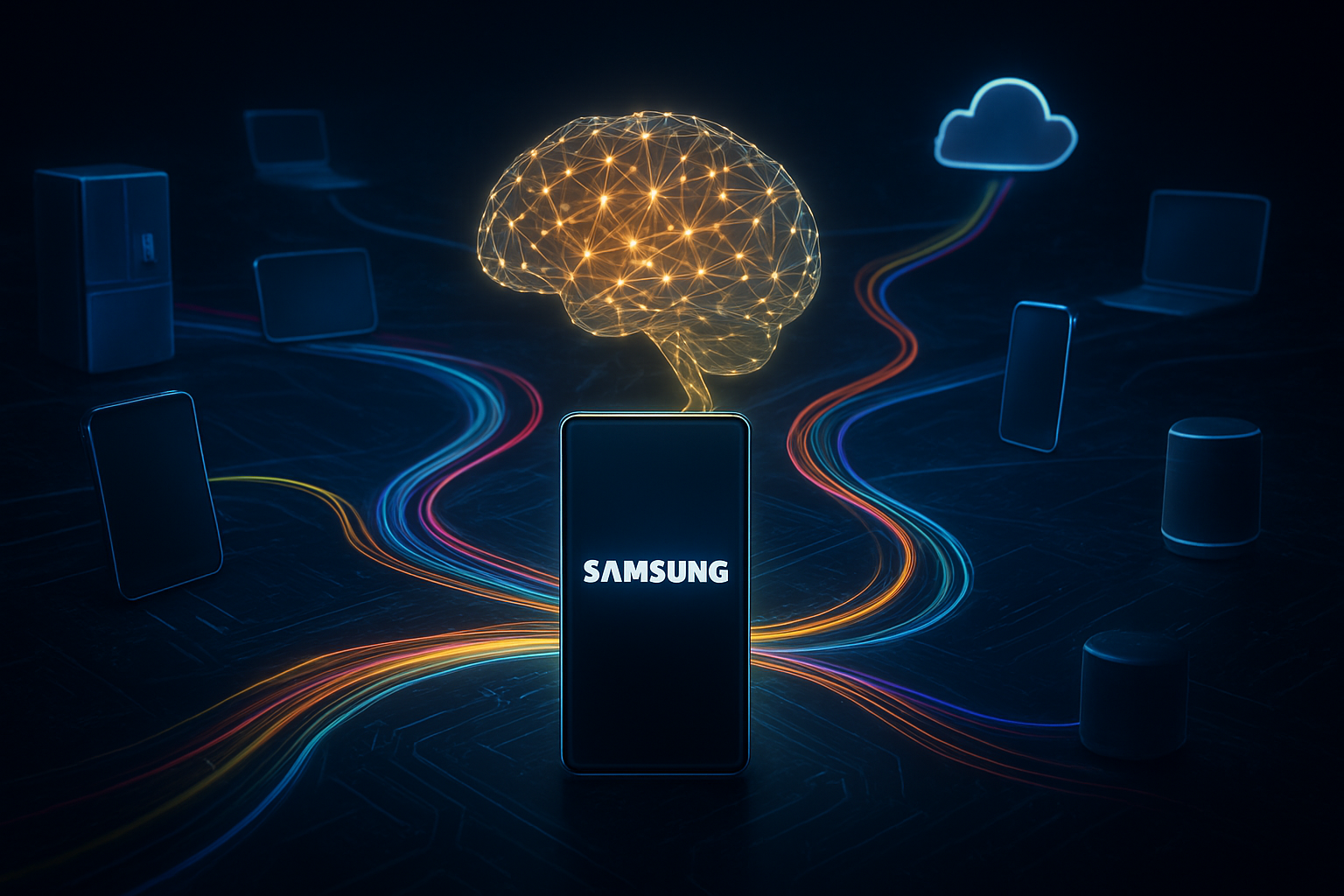
Tag: Samsung

  • Samsung’s 800 Million Device Moonshot: The AI Ecosystem Revolution Led by Gemini 3 and Perplexity

    Samsung’s 800 Million Device Moonshot: The AI Ecosystem Revolution Led by Gemini 3 and Perplexity

    In a bold move to dominate the next era of personal computing, Samsung Electronics Co., Ltd. (KRX: 005930) has officially announced an ambitious roadmap to bring its "Galaxy AI" suite to 800 million devices by the end of 2026. This target, revealed by co-CEO T.M. Roh in early January 2026, represents a massive doubling of the company’s 2025 goals and signals a shift from AI as a premium smartphone feature to a ubiquitous "ambient layer" across the world’s largest consumer electronics ecosystem.

    The announcement marks a pivotal moment for the industry, as Samsung moves beyond simple chatbots to integrate sophisticated, multi-modal intelligence into everything from the upcoming Galaxy S26 flagship to smart refrigerators and Micro LED televisions. By leveraging deep-tier partnerships with Alphabet Inc. (NASDAQ: GOOGL) and the rising search giant Perplexity AI, Samsung is positioning itself as the primary gatekeeper for consumer AI, aiming to outpace competitors through sheer scale and cross-device synergy.

    The Technical Backbone: Gemini 3 and the Rebirth of Bixby

    At the heart of Samsung’s 2026 expansion is the integration of Google’s recently released Gemini 3 model. Unlike its predecessors, Gemini 3 offers significantly enhanced on-device processing capabilities, allowing Galaxy devices to handle complex multi-modal tasks—such as real-time video analysis and sophisticated reasoning—without constantly relying on the cloud. This integration powers the new "Bixby Live" feature in One UI 8.5, which introduces eight specialized AI agents capable of everything from acting as a real-time "Storyteller" for children to a "Dress Matching" fashion consultant that uses the device's camera to analyze a user's wardrobe.

    The partnership with Perplexity AI addresses one of Bixby’s long-standing hurdles: the "hallucination" and limited knowledge of traditional voice assistants. By integrating Perplexity’s real-time search engine, Bixby can now function as a professional researcher, providing cited, up-to-the-minute answers to complex queries. Furthermore, the 2026 appliance lineup, including the Bespoke AI Refrigerator Family Hub, utilizes Gemini 3-powered AI Vision to recognize over 1,500 food items, automatically tracking expiration dates and suggesting recipes. This is a significant leap from the 2024 models, which were limited to basic image recognition for a few dozen items.

    A New Power Dynamic in the AI Arms Race

    Samsung’s aggressive 800-million-device goal creates a formidable challenge for Apple Inc. (NASDAQ: AAPL), whose "Apple Intelligence" has remained largely focused on the iPhone and Mac ecosystems. By embedding high-end AI into mid-range A-series phones and home appliances, Samsung is effectively "democratizing" advanced AI, forcing competitors to either lower their hardware requirements or risk losing market share in the burgeoning smart home sector. Google also stands as a primary beneficiary; through Samsung, Gemini 3 gains a massive hardware distribution channel that rivals the reach of Microsoft (NASDAQ: MSFT) and its Windows Copilot integration.

    For Perplexity, the partnership is a strategic masterstroke, granting the startup immediate access to hundreds of millions of users and positioning it as a viable alternative to traditional search. This collaboration disrupts the existing search paradigm, as users increasingly turn to their voice assistants for cited information rather than clicking through blue links on a browser. Industry experts suggest that if Samsung successfully hits its 2026 target, it will control the most diverse data set in the AI industry, spanning mobile usage, home habits, and media consumption.

    Ambient Intelligence and the Privacy Frontier

    The shift toward "Ambient AI"—where intelligence is integrated into the physical environment through TVs and appliances—marks a departure from the "screen-first" era of the last decade. Samsung’s use of Voice ID technology allows its 2026 appliances to recognize individual family members by their vocal prints, delivering personalized schedules and health data. While this offers unprecedented convenience, it also raises significant concerns regarding data privacy and the "always-listening" nature of 800 million connected microphones.

    Samsung has attempted to mitigate these concerns by emphasizing its "Knox Matrix" security, which uses blockchain-based encryption to keep sensitive AI processing on-device or within a private home network. However, as AI becomes an invisible layer of daily life, the industry is watching closely to see how Samsung balances its massive data harvesting needs with the increasing global demand for digital sovereignty. This milestone echoes the early days of the smartphone revolution, but with the stakes raised by the predictive and autonomous nature of generative AI.

    The Road to 2027: What Lies Ahead

    Looking toward the latter half of 2026, the launch of the Galaxy S26 and the rumored "Galaxy Z TriFold" will be the true litmus tests for Samsung’s AI ambitions. These devices are expected to debut with "Hey Plex" as a native wake-word option, further blurring the lines between hardware and AI services. Experts predict that the next frontier for Samsung will be "Autonomous Task Orchestration," where Bixby doesn't just answer questions but executes multi-step workflows across devices—such as ordering groceries when the fridge is low and scheduling a delivery time that fits the user’s calendar.

    The primary challenge remains the "utility gap"—ensuring that these 800 million devices provide meaningful value rather than just novelty features. As the AI research community moves toward "Agentic AI," Samsung’s hardware variety provides a unique laboratory for testing how AI can assist in physical tasks. If the company can maintain its current momentum, the end of 2026 could mark the year that artificial intelligence officially moved from our pockets into the very fabric of our homes.

    Final Thoughts: A Defining Moment for Samsung

    Samsung’s 800 million device goal is more than just a sales target; it is a declaration of intent to define the AI era. By combining the software prowess of Google and Perplexity with its own unparalleled hardware manufacturing scale, Samsung is building a moat that few can cross. The integration of Gemini 3 and the transformation of Bixby represent a total reimagining of the user interface, moving us closer to a world where technology anticipates our needs without being asked.

    As we move through 2026, the tech world will be watching the adoption rates of One UI 8.5 and the performance of the new Bespoke AI appliances. The success of this "Moonshot" will likely determine the hierarchy of the tech industry for the next decade. For now, Samsung has laid down a gauntlet that demands a response from every major player in Silicon Valley and beyond.


    This content is intended for informational purposes only and represents analysis of current AI developments.

    TokenRing AI delivers enterprise-grade solutions for multi-agent AI workflow orchestration, AI-powered development tools, and seamless remote collaboration platforms.
    For more information, visit https://www.tokenring.ai/.

  • The HBM4 Memory Supercycle: The Trillion-Dollar War Powering the Next Frontier of AI

    The HBM4 Memory Supercycle: The Trillion-Dollar War Powering the Next Frontier of AI

    The artificial intelligence revolution has reached a critical hardware inflection point as 2026 begins. While the last two years were defined by the scramble for high-end GPUs, the industry has now shifted its gaze toward the "memory wall"—the bottleneck where data processing speeds outpace the ability of memory to feed that data to the processor. Enter the HBM4 (High Bandwidth Memory 4) supercycle, a generational leap in semiconductor technology that is fundamentally rewriting the rules of AI infrastructure. This week, the competition reached a fever pitch as the world’s three dominant memory makers—SK Hynix, Samsung, and Micron—unveiled their final production roadmaps for the chips that will power the next decade of silicon.

    The significance of this transition cannot be overstated. As large language models (LLMs) scale toward 100 trillion parameters, the demand for massive, ultra-fast memory has transitioned HBM from a specialized component into a strategic, custom asset. With NVIDIA (NASDAQ: NVDA) recently detailing its HBM4-exclusive "Rubin" architecture at CES 2026, the race to supply these chips has become the most expensive and technologically complex battle in the history of the semiconductor industry.

    The Technical Leap: 2 TB/s and the 2048-Bit Frontier

    HBM4 represents the most significant architectural overhaul in the history of high-bandwidth memory, moving beyond incremental speed bumps to a complete redesign of the memory interface. The most striking advancement is the doubling of the memory interface width from the 1024-bit bus used in HBM3e to a massive 2048-bit bus. This allows individual HBM4 stacks to achieve staggering bandwidths of 2.0 TB/s to 2.8 TB/s per stack—nearly triple the performance of the early HBM3 modules that powered the first wave of the generative AI boom.

    Beyond raw speed, the industry is witnessing a shift toward extreme 3D stacking. While 12-layer stacks (36GB) are the baseline for initial mass production in early 2026, the "holy grail" is the 16-layer stack, providing up to 64GB of capacity per module. To achieve this within the strict 775µm height limit set by JEDEC, manufacturers are thinning DRAM wafers to roughly 30 micrometers—about one-third the thickness of a human hair. This has necessitated a move toward "Hybrid Bonding," a process where copper pads are fused directly to copper without the use of traditional micro-bumps, significantly reducing stack height and improving thermal dissipation.

    Furthermore, the "base die" at the bottom of the HBM stack has evolved. No longer a simple interface, it is now a high-performance logic die manufactured on advanced foundry nodes like 5nm or 4nm. This transition marks the first time memory and logic have been so deeply integrated, effectively turning the memory stack into a co-processor that can handle basic data operations before they even reach the main GPU.

    The Three-Way War: SK Hynix, Samsung, and Micron

    The competitive landscape for HBM4 is a high-stakes triangle between three giants. SK Hynix (KRX: 000660), the current market leader with over 50% market share, has solidified its position through a "One-Team" alliance with TSMC (NYSE: TSM). By leveraging TSMC’s advanced logic dies and its own Mass Reflow Molded Underfill (MR-MUF) bonding technology, SK Hynix aims to begin volume shipments of 12-layer HBM4 by the end of Q1 2026. Their 16-layer prototype, showcased earlier this month, is widely considered the frontrunner for NVIDIA's high-end Rubin R100 GPUs.

    Samsung Electronics (KRX: 005930), after trailing in the HBM3e generation, is mounting a massive counter-offensive. Samsung’s unique advantage is its "turnkey" capability; it is the only company capable of designing the DRAM, manufacturing the logic die in its internal 4nm foundry, and handling the advanced 3D packaging under one roof. This vertical integration has allowed Samsung to claim industry-leading yields for its 16-layer HBM4, which is currently undergoing final qualification for the 2026 Rubin launch.

    Meanwhile, Micron Technology (NASDAQ: MU) has positioned itself as the performance leader, claiming its HBM4 stacks can hit 2.8 TB/s using its proprietary 1-beta DRAM process. Micron’s strategy has been focused on energy efficiency, a critical factor for massive data centers facing power constraints. The company recently announced that its entire HBM4 capacity for 2026 is already sold out, highlighting the desperate demand from hyperscalers like Google, Meta, and Microsoft who are building their own custom AI accelerators.

    Breaking the Memory Wall and Market Disruption

    The HBM4 supercycle is more than a hardware upgrade; it is the solution to the "Memory Wall" that has threatened to stall AI progress. By providing the massive bandwidth required to feed data to thousands of parallel cores, HBM4 enables the training of models with 10 to 100 times the complexity of GPT-4. This shift is expected to accelerate the development of "World Models" and sophisticated agentic AI systems that require real-time processing of multimodal data.

    However, this focus on high-margin HBM4 is causing significant ripples across the broader tech economy. To meet the demand for HBM4, manufacturers are diverting massive amounts of wafer capacity away from traditional DDR5 and mobile memory. As of January 2026, standard PC and server RAM prices have spiked by nearly 300% year-over-year, as the industry prioritizes the lucrative AI market. This "wafer cannibalization" is making high-end gaming PCs and enterprise servers significantly more expensive, even as AI capabilities skyrocket.

    Furthermore, the move toward "Custom HBM" (cHBM) is disrupting the traditional relationship between memory makers and chip designers. For the first time, major AI labs are requesting bespoke memory configurations with specific logic embedded in the base die. This shift is turning memory into a semi-custom product, favoring companies like Samsung and the SK Hynix-TSMC alliance that can offer deep integration between logic and storage.

    The Horizon: Custom Logic and the Road to HBM5

    Looking ahead, the HBM4 era is expected to last until late 2027, with "HBM4E" (Extended) already in the research phase. The next major milestone will be the full adoption of "Logic-on-Memory," where specific AI kernels are executed directly within the memory stack to minimize data movement—the most energy-intensive part of AI computing. Experts predict this will lead to a 50% reduction in total system power consumption for inference tasks.

    The long-term roadmap also points toward HBM5, which is rumored to explore even more exotic materials and optical interconnects to break the 5 TB/s barrier. However, the immediate challenge remains manufacturing yield. The complexity of thinning wafers and hybrid bonding is so high that even a minor defect can ruin an entire 16-layer stack worth thousands of dollars. Perfecting these manufacturing processes will be the primary focus for engineers throughout the remainder of 2026.

    A New Era of Silicon Synergy

    The HBM4 supercycle represents a fundamental shift in how we build computers. For decades, the processor was the undisputed king of the system, with memory serving as a secondary, commodity component. In the age of generative AI, that hierarchy has dissolved. Memory is now the heartbeat of the AI cluster, and the ability to produce HBM4 at scale has become a matter of national and corporate security.

    As we move into the second half of 2026, the industry will be watching the rollout of NVIDIA’s Rubin systems and the first wave of 16-layer HBM4 deployments. The winner of this "Memory War" will not only reap tens of billions in revenue but will also dictate the pace of AI evolution for the next decade. For now, SK Hynix holds the lead, Samsung has the scale, and Micron has the efficiency—but in the volatile world of semiconductors, the crown is always up for grabs.


    This content is intended for informational purposes only and represents analysis of current AI developments.

    TokenRing AI delivers enterprise-grade solutions for multi-agent AI workflow orchestration, AI-powered development tools, and seamless remote collaboration platforms.
    For more information, visit https://www.tokenring.ai/.

  • Beyond Blackwell: Inside Nvidia’s ‘Vera Rubin’ Revolution and the War on ‘Computation Inflation’

    Beyond Blackwell: Inside Nvidia’s ‘Vera Rubin’ Revolution and the War on ‘Computation Inflation’

    As the artificial intelligence landscape shifts from simple chatbots to complex agentic reasoning and physical robotics, Nvidia (NASDAQ: NVDA) has officially moved into full production of its next-generation "Vera Rubin" platform. Named after the pioneering astronomer who provided the first evidence of dark matter, the Rubin architecture is more than just a faster chip; it represents a fundamental pivot in the company’s roadmap. By shifting to a relentless one-year product cycle, Nvidia is attempting to outpace a phenomenon CEO Jensen Huang calls "computation inflation," where the exponential growth of AI model complexity threatens to outstrip the physical and economic limits of current hardware.

    The arrival of the Vera Rubin platform in early 2026 marks the end of the two-year "Moore’s Law" cadence that defined the semiconductor industry for decades. With the R100 GPU and the custom "Vera" CPU at its core, Nvidia is positioning itself not just as a chipmaker, but as the architect of the "AI Factory." This transition is underpinned by a strategic technical shift toward High-Bandwidth Memory (HBM4) integration, involving a high-stakes partnership with Samsung Electronics (KRX: 005930) to secure the massive volumes of silicon required to power the next trillion-parameter frontier.

    The Silicon of 2026: R100, Vera CPUs, and the HBM4 Breakthrough

    At the heart of the Vera Rubin platform is the R100 GPU, a marvel of engineering fabricated on Taiwan Semiconductor Manufacturing Company's (NYSE: TSM) enhanced 3nm (N3P) process. Moving away from the monolithic designs of the past, the R100 utilizes a modular chiplet architecture on a massive 100x100mm substrate. This design allows for approximately 336 billion transistors—a 1.6x increase over the previous Blackwell generation—delivering a staggering 50 PFLOPS of FP4 inference performance per GPU. To put this in perspective, a single rack of Rubin-powered servers (the NVL144) can now reach 3.6 ExaFLOPS of compute, effectively turning a single data center row into a supercomputer that would have been unimaginable just three years ago.

    The most critical technical leap, however, is the integration of HBM4 memory. As AI models grow, they hit a "memory wall" where the speed of data transfer between the processor and memory becomes the primary bottleneck. Rubin addresses this by featuring 288GB of HBM4 memory per GPU, providing a bandwidth of up to 22 TB/s. This is achieved through an eighth-stack configuration and a widened 2,048-bit memory interface, nearly doubling the throughput of the Blackwell Ultra refresh. To ensure a steady supply of these advanced modules, Nvidia has deepened its collaboration with Samsung, which is utilizing its 6th-generation 10nm-class (1c) DRAM process to produce HBM4 chips that are 40% more energy-efficient than their predecessors.

    Beyond the GPU, Nvidia is introducing the Vera CPU, the successor to the Grace processor. Unlike Grace, which relied on standard Arm Neoverse cores, Vera features 88 custom "Olympus" Arm cores designed specifically for agentic AI workflows. These cores are optimized for the complex "thinking" chains required by autonomous agents that must plan and reason before acting. Coupled with the new BlueField-4 DPU for high-speed networking and the sixth-generation NVLink 6 interconnect—which offers 3.6 TB/s of bidirectional bandwidth—the Rubin platform functions as a unified, vertically integrated system rather than a collection of disparate parts.

    Reshaping the Competitive Landscape: The AI Factory Arms Race

    The shift to an annual update cycle is a strategic masterstroke designed to keep competitors like Advanced Micro Devices (NASDAQ: AMD) and Intel (NASDAQ: INTC) in a perpetual state of catch-up. While AMD’s Instinct MI400 series, expected later in 2026, boasts higher raw memory capacity (up to 432GB), Nvidia’s Rubin counters with superior compute density and a more mature software ecosystem. The "CUDA moat" remains Nvidia’s strongest defense, as the Rubin platform is designed to be a "turnkey" solution for hyperscalers like Microsoft (NASDAQ: MSFT), Meta (NASDAQ: META), and Alphabet (NASDAQ: GOOGL). These tech giants are no longer just buying chips; they are deploying entire "AI Factories" that can reduce the cost of inference tokens by 10x compared to previous years.

    For these hyperscalers, the Rubin platform represents a path to sustainable scaling. By reducing the number of GPUs required to train Mixture-of-Experts (MoE) models by a factor of four, Nvidia allows these companies to scale their models to 100 trillion parameters without a linear increase in their physical data center footprint. This is particularly vital for Meta and Google, which are racing to integrate "Agentic AI" into every consumer product. The specialized Rubin CPX variant, which uses more affordable GDDR7 memory for the "context phase" of inference, further allows these companies to process millions of tokens of context more economically, making "long-context" AI a standard feature rather than a luxury.

    However, the aggressive one-year rhythm also places immense pressure on the global supply chain. By qualifying Samsung as a primary HBM4 supplier alongside SK Hynix (KRX: 000660) and Micron Technology (NASDAQ: MU), Nvidia is attempting to avoid the shortages that plagued the H100 and Blackwell launches. This diversification is a clear signal that Nvidia views memory availability—not just compute power—as the defining constraint of the 2026 AI economy. Samsung’s ability to hit its target of 250,000 wafers per month will be the linchpin of the Rubin rollout.

    Deflating ‘Computation Inflation’ and the Rise of Physical AI

    Jensen Huang’s concept of "computation inflation" addresses a looming crisis: the volume of data and the complexity of AI models are growing at roughly 10x per year, while traditional CPU performance has plateaued. Without the massive architectural leaps provided by Rubin, the energy and financial costs of AI would become unsustainable. Nvidia’s strategy is to "deflate" the cost of intelligence by delivering 1000x more compute every few years through a combination of GPU/CPU co-design and new data types like NVFP4. This focus on efficiency is evident in the Rubin NVL72 rack, which is designed to be 100% liquid-cooled, eliminating the need for energy-intensive water chillers and saving up to 6% in total data center power consumption.

    The Rubin platform also serves as the hardware foundation for "Physical AI"—AI that interacts with the physical world. Through its Cosmos foundation models, Nvidia is using Rubin-powered clusters to generate synthetic 3D data grounded in physics, which is then used to train humanoid robots and autonomous vehicles. This marks a transition from AI that merely predicts the next word to AI that understands the laws of physics. For companies like Tesla (NASDAQ: TSLA) or the robotics startups of 2026, the R100’s ability to handle "test-time scaling"—where the model spends more compute cycles "thinking" before executing a physical movement—is a prerequisite for safe and reliable automation.

    This wider significance cannot be overstated. By providing the compute necessary for models to "reason" in real-time, Nvidia is moving the industry toward the era of autonomous agents. This mirrors previous milestones like the introduction of the Transformer model in 2017 or the launch of ChatGPT in 2022, but with a focus on agency and physical interaction. The concern, however, remains the centralization of this power. As Nvidia becomes the "operating system" for AI infrastructure, the industry’s dependence on a single vendor’s roadmap has never been higher.

    The Road Ahead: From Rubin Ultra to Feynman

    Looking toward the near-term future, Nvidia has already teased the "Rubin Ultra" for 2027, which will feature 16-high HBM4 stacks and even greater memory capacity. Beyond that lies the "Feynman" architecture, scheduled for 2028, which is rumored to explore even more exotic packaging technologies and perhaps the first steps toward optical interconnects at the chip level. The immediate challenge for 2026, however, will be the massive transition to liquid cooling. Most existing data centers were designed for air cooling, and the shift to the fully liquid-cooled Rubin racks will require a multi-billion dollar overhaul of global infrastructure.

    Experts predict that the next two years will see a "disaggregation" of AI workloads. We will likely see specialized clusters where Rubin R100s handle the heavy lifting of training and complex reasoning, while Rubin CPX units handle massive context processing, and smaller edge-AI chips manage simple tasks. The challenge for Nvidia will be maintaining this frantic annual pace without sacrificing reliability or software stability. If they succeed, the "cost per token" could drop so low that sophisticated AI agents become as ubiquitous and inexpensive as a Google search.

    A New Era of Accelerated Computing

    The launch of the Vera Rubin platform is a watershed moment in the history of computing. It represents the successful execution of a strategy to compress decades of technological progress into a single-year cycle. By integrating custom CPUs, advanced HBM4 memory from Samsung, and next-generation interconnects, Nvidia has built a fortress that will be difficult for any competitor to storm in the near future. The key takeaway is that the "AI chip" is dead; we are now in the era of the "AI System," where the rack is the unit of compute.

    As we move through 2026, the industry will be watching two things: the speed of liquid-cooling adoption in enterprise data centers and the real-world performance of Agentic AI powered by the Vera CPU. If Rubin delivers on its promise of a 10x reduction in token costs, it will not just deflate "computation inflation"—it will ignite a new wave of economic productivity driven by autonomous, reasoning machines. For now, Nvidia remains the undisputed architect of this new world, with the Vera Rubin platform serving as its most ambitious blueprint yet.


    This content is intended for informational purposes only and represents analysis of current AI developments.

    TokenRing AI delivers enterprise-grade solutions for multi-agent AI workflow orchestration, AI-powered development tools, and seamless remote collaboration platforms.
    For more information, visit https://www.tokenring.ai/.

  • Samsung’s 2nm Triumph: How the Snapdragon 8 Gen 5 Deal Marks a Turning Point in the Foundry Wars

    Samsung’s 2nm Triumph: How the Snapdragon 8 Gen 5 Deal Marks a Turning Point in the Foundry Wars

    In a move that has sent shockwaves through the global semiconductor industry, Samsung Electronics (KRX: 005930) has officially secured a landmark deal to produce Qualcomm’s (NASDAQ: QCOM) next-generation Snapdragon 8 Gen 5 processors on its cutting-edge 2-nanometer (SF2) production node. Announced during the opening days of CES 2026, the partnership signals a dramatic resurgence for Samsung Foundry, which has spent the better part of the last three years trailing behind the market leader, Taiwan Semiconductor Manufacturing Company (NYSE: TSM). This deal is not merely a supply chain adjustment; it represents a fundamental shift in the competitive landscape of high-end silicon, validating Samsung’s long-term bet on a radical new transistor architecture.

    The immediate significance of this announcement cannot be overstated. For Qualcomm, the move to Samsung’s SF2 node for its flagship "Snapdragon 8 Elite Gen 5" (codenamed SM8850s) marks a return to a dual-sourcing strategy designed to mitigate "TSMC risk"—a combination of soaring wafer costs and capacity constraints driven by Apple’s (NASDAQ: AAPL) dominance of TSMC’s 2nm lines. For the broader tech industry, the deal serves as the first major real-world validation of Gate-All-Around (GAA) technology at scale, proving that Samsung has finally overcome the yield hurdles that plagued its earlier 3nm and 4nm efforts.

    The Technical Edge: GAA and the Backside Power Advantage

    At the heart of Samsung’s resurgence is its proprietary Multi-Bridge Channel FET (MBCFET™) architecture, a specific implementation of Gate-All-Around (GAA) technology. While TSMC is just now transitioning to its first generation of GAA (Nanosheet) with its N2 node, Samsung is already entering its third generation of GAA with the SF2 process. This two-year lead in GAA experience has allowed Samsung to refine the geometry of its nanosheets, enabling wider channels that can be tuned for significantly higher performance or lower power consumption depending on the chip’s requirements.

    Technically, the SF2 node offers a staggering 12% increase in performance and a 25% improvement in power efficiency over previous 3nm iterations. However, the true "secret sauce" in the Snapdragon 8 Gen 5 production is Samsung’s early implementation of Backside Power Delivery Network (BSPDN) optimizations. By moving the power rails to the back of the wafer, Samsung has eliminated the "IR drop" (voltage drop) and signal congestion that typically limits clock speeds in high-performance mobile chips. This allows the Snapdragon 8 Gen 5 to maintain peak performance longer without thermal throttling—a critical requirement for the next generation of AI-heavy smartphones.

    Initial reactions from the semiconductor research community have been cautiously optimistic. Analysts note that while TSMC still holds a slight lead in absolute transistor density—roughly 235 million transistors per square millimeter compared to Samsung’s 200 million—the gap has narrowed significantly. More importantly, Samsung’s SF2 yields have reportedly stabilized in the 50% to 60% range. While still below TSMC’s gold-standard 80%, this is a massive leap from the sub-20% yields that derailed Samsung’s 3nm launch in 2024, making the SF2 node commercially viable for high-volume flagship devices like the upcoming Galaxy Z Fold 8.

    Disrupting the Monopoly: Competitive Implications for Tech Giants

    The Samsung-Qualcomm deal creates a new power dynamic in the "foundry wars." For years, TSMC has enjoyed a near-monopoly on the most advanced nodes, allowing it to command premium prices. Reports from late 2025 indicated that TSMC’s 2nm wafers were priced at an eye-watering $30,000 each. Samsung has aggressively countered this by offering its SF2 wafers for approximately $20,000, providing a 33% cost advantage that is irresistible to fabless chipmakers like Qualcomm and potentially NVIDIA (NASDAQ: NVDA).

    NVIDIA, in particular, is reportedly watching the Samsung-Qualcomm partnership with intense interest. As TSMC’s capacity remains bottlenecked by Apple and the insatiable demand for Blackwell-successor AI GPUs, NVIDIA is rumored to be in active testing with Samsung’s SF2 node for its next generation of consumer-grade GeForce GPUs and specialized AI ASICs. By diversifying its supply chain, NVIDIA could avoid the "Apple tax" and ensure a more stable supply of silicon for the burgeoning AI PC market.

    Meanwhile, for Apple, Samsung’s resurgence acts as a necessary "price ceiling." Even if Apple remains an exclusive TSMC customer for its A20 and M6 chips, the existence of a viable 2nm alternative at Samsung prevents TSMC from exerting absolute pricing power. This competitive pressure is expected to accelerate the roadmap for all players, forcing TSMC to expedite its own 1.6nm (A16) node to maintain its lead.

    The Era of Agentic AI and Sovereign Foundries

    The broader significance of Samsung’s 2nm success lies in its alignment with two major trends: the rise of "Agentic AI" and the push for "sovereign" semiconductor manufacturing. The Snapdragon 8 Gen 5 is engineered specifically for agentic AI—autonomous AI agents that can navigate apps and perform tasks on a user’s behalf. This requires massive on-device processing power; the SF2-produced chip reportedly delivers a 113% boost in Generative AI processing and can handle 220 tokens per second for on-device Large Language Models (LLMs).

    Furthermore, Samsung’s pivot of its $44 billion Taylor, Texas, facility to prioritize 2nm production has significant geopolitical implications. By producing Qualcomm’s flagship chips on U.S. soil, Samsung is positioning itself as a "sovereign foundry" for American tech giants. This move aligns with the goals of the CHIPS Act and provides a strategic alternative to Taiwan-based manufacturing, which remains a point of concern for some Western policymakers and corporate boards.

    Comparatively, this milestone is being likened to the "45nm era" of the late 2000s, when the industry last saw a major shift in transistor materials (High-K Metal Gate). The transition to GAA is a similarly fundamental change, and Samsung’s ability to execute on it first gives them a psychological and technical edge that could define the next decade of mobile and AI computing.

    Looking Ahead: The Road to 1.4nm and Beyond

    As Samsung Foundry regains its footing, the focus is already shifting toward the 1.4nm (SF1.4) node, scheduled for mass production in 2026. Experts predict that the lessons learned from the 2nm SF2 node—particularly regarding GAA nanosheet stability and Backside Power Delivery—will be the foundation for Samsung’s next decade of growth. The company is also heavily investing in 3D IC packaging technologies, which will allow for the vertical stacking of logic and memory, further boosting AI performance.

    However, challenges remain. Samsung must continue to improve its yield rates to match TSMC’s efficiency, and it must prove that its SF2 chips can maintain long-term reliability in the field. The upcoming launch of the Galaxy S26 and Z Fold 8 series will be the ultimate "litmus test" for the Snapdragon 8 Gen 5. If these devices deliver on their performance and battery life promises without the overheating issues of the past, Samsung may well reclaim its title as a co-leader in the semiconductor world.

    A New Chapter in Silicon History

    The deal between Samsung and Qualcomm for 2nm production is a watershed moment that officially ends the era of TSMC’s uncontested dominance at the bleeding edge. By successfully iterating on its GAA architecture and offering a compelling price-to-performance ratio, Samsung has re-established itself as a top-tier foundry capable of supporting the world’s most demanding AI applications.

    Key takeaways from this development include the validation of MBCFET technology, the strategic importance of U.S.-based manufacturing in Texas, and the arrival of highly efficient, on-device agentic AI. As we move through 2026, the industry will be watching closely to see if other giants like NVIDIA or even Intel (NASDAQ: INTC) follow Qualcomm’s lead. For now, the "foundry wars" have entered a new, more balanced chapter, promising faster innovation and more competitive pricing for the entire AI ecosystem.


    This content is intended for informational purposes only and represents analysis of current AI developments.

    TokenRing AI delivers enterprise-grade solutions for multi-agent AI workflow orchestration, AI-powered development tools, and seamless remote collaboration platforms.
    For more information, visit https://www.tokenring.ai/.

  • The HBM4 Memory War: SK Hynix, Samsung, and Micron Clash at CES 2026 to Power NVIDIA’s Rubin Revolution

    The HBM4 Memory War: SK Hynix, Samsung, and Micron Clash at CES 2026 to Power NVIDIA’s Rubin Revolution

    The 2026 Consumer Electronics Show (CES) in Las Vegas has transformed from a showcase of consumer gadgets into the primary battlefield for the most critical component in the artificial intelligence era: High Bandwidth Memory (HBM). As of January 8, 2026, the industry is witnessing the eruption of the "HBM4 Memory War," a high-stakes conflict between the world’s three largest memory manufacturers—SK Hynix (KRX: 000660), Samsung Electronics (KRX: 005930), and Micron Technology (NASDAQ: MU). This technological arms race is not merely about storage; it is a desperate sprint to provide the massive data throughput required by NVIDIA’s (NASDAQ: NVDA) newly detailed "Rubin" platform, the successor to the record-breaking Blackwell architecture.

    The significance of this development cannot be overstated. As AI models grow to trillions of parameters, the bottleneck has shifted from raw compute power to memory bandwidth and energy efficiency. The announcements made this week at CES 2026 signal a fundamental shift in semiconductor architecture, where memory is no longer a passive storage bin but an active, logic-integrated component of the AI processor itself. With billions of dollars in capital expenditure on the line, the winners of this HBM4 cycle will likely dictate the pace of AI advancement for the remainder of the decade.

    Technical Frontiers: 16-Layer Stacks and the 1c Process

    The technical specifications unveiled at CES 2026 represent a monumental leap over the previous HBM3E standard. SK Hynix stole the early headlines by debuting the world’s first 16-layer 48GB HBM4 module. To achieve this, the company utilized its proprietary Advanced Mass Reflow Molded Underfill (MR-MUF) technology, thinning individual DRAM wafers to a staggering 30 micrometers to fit within the strict 775µm height limit set by JEDEC. This 16-layer stack delivers an industry-leading data rate of 11.7 Gbps per pin, which, when integrated into an 8-stack system like NVIDIA’s Rubin, provides a system-level bandwidth of 22 TB/s—nearly triple that of early HBM3E systems.

    Samsung Electronics countered with a focus on manufacturing sophistication and efficiency. Samsung’s HBM4 is built on its "1c" nanometer process (the 6th generation of 10nm-class DRAM). By moving to this advanced node, Samsung claims a 40% improvement in energy efficiency over its competitors. This is a critical advantage for data center operators struggling with the thermal demands of GPUs that now exceed 1,000 watts. Unlike its rivals, Samsung is leveraging its internal foundry to produce the HBM4 logic base die using a 10nm logic process, positioning itself as a "one-stop shop" that controls the entire stack from the silicon to the final packaging.

    Micron Technology, meanwhile, showcased its aggressive capacity expansion and its role as a lead partner for the initial Rubin launch. Micron’s HBM4 entry focuses on a 12-high (12-Hi) 36GB stack that emphasizes a 2048-bit interface—double the width of HBM3E. This allows for speeds exceeding 2.0 TB/s per stack while maintaining a 20% power efficiency gain over previous generations. The industry reaction has been one of collective awe; experts from the AI research community note that the shift from memory-based nodes to logic nodes (like TSMC’s 5nm for the base die) effectively turns HBM4 into a "custom" memory solution that can be tailored for specific AI workloads.

    The Kingmaker: NVIDIA’s Rubin Platform and the Supply Chain Scramble

    The primary driver of this memory frenzy is NVIDIA’s Rubin platform, which was the centerpiece of the CES 2026 keynote. The Rubin R100 and R200 GPUs, built on TSMC’s (NYSE: TSM) 3nm process, are designed to consume HBM4 at an unprecedented scale. Each Rubin GPU is expected to utilize eight stacks of HBM4, totaling 288GB of memory per chip. To ensure it does not repeat the supply shortages that plagued the Blackwell launch, NVIDIA has reportedly secured massive capacity commitments from all three major vendors, effectively acting as the kingmaker in the semiconductor market.

    Micron has responded with the most aggressive capacity expansion in its history, targeting a dedicated HBM4 production capacity of 15,000 wafers per month by the end of 2026. This is part of a broader $20 billion capital expenditure plan that includes new facilities in Taiwan and a "megaplant" in Hiroshima, Japan. By securing such a large slice of the Rubin supply chain, Micron is moving from its traditional "third-place" position to a primary supplier status, directly challenging the dominance of SK Hynix.

    The competitive implications extend beyond the memory makers. For AI labs and tech giants like Google (NASDAQ: GOOGL), Meta (NASDAQ: META), and Microsoft (NASDAQ: MSFT), the availability of HBM4-equipped Rubin GPUs will determine their ability to train next-generation "Agentic AI" models. Companies that can secure early allocations of these high-bandwidth systems will have a strategic advantage in inference speed and cost-per-query, potentially disrupting existing SaaS products that are currently limited by the latency of older hardware.

    A Paradigm Shift: From Compute-Centric to Memory-Centric AI

    The "HBM4 War" marks a broader shift in the AI landscape. For years, the industry focused on "Teraflops"—the number of floating-point operations a processor could perform. However, as models have grown, the energy cost of moving data between the processor and memory has become the primary constraint. The integration of logic dies into HBM4, particularly through the SK Hynix and TSMC "One-Team" alliance, signifies the end of the compute-only era. By embedding memory controllers and physical layer interfaces directly into the memory stack, manufacturers are reducing the physical distance data must travel, thereby slashing latency and power consumption.

    This development also brings potential concerns regarding market consolidation. The technical complexity and capital requirements of HBM4 are so high that smaller players are being priced out of the market entirely. We are seeing a "triopoly" where SK Hynix, Samsung, and Micron hold all the cards. Furthermore, the reliance on advanced packaging techniques like Hybrid Bonding and MR-MUF creates a new set of manufacturing risks; any yield issues at these nanometer scales could lead to global shortages of AI hardware, stalling progress in fields from drug discovery to climate modeling.

    Comparisons are already being drawn to the 2023 "GPU shortage," but with a twist. While 2023 was about the chips themselves, 2026 is about the interconnects and the stacking. The HBM4 breakthrough is arguably more significant than the jump from H100 to B100, as it addresses the fundamental "memory wall" that has threatened to plateau AI scaling laws.

    The Horizon: Rubin Ultra and the Road to 1TB Per GPU

    Looking ahead, the roadmap for HBM4 is already extending into 2027 and beyond. During the CES presentations, hints were dropped regarding the "Rubin Ultra" refresh, which is expected to move to 16-high HBM4e (Extended) stacks. This would effectively double the memory capacity again, potentially allowing for 1 terabyte of HBM memory on a single GPU package. Micron and SK Hynix are already sampling these 16-Hi stacks, with mass production targets set for early 2027.

    The next major challenge will be the move to "Custom HBM" (cHBM), where AI companies like OpenAI or Tesla (NASDAQ: TSLA) may design their own proprietary logic dies to be manufactured by TSMC and then stacked with DRAM by SK Hynix or Micron. This level of vertical integration would allow for AI-specific optimizations that are currently impossible with off-the-shelf components. Experts predict that by 2028, the distinction between "processor" and "memory" will have blurred so much that we may begin referring to them as unified "AI Compute Cubes."

    Final Reflections on the Memory-First Era

    The events at CES 2026 have made one thing clear: the future of artificial intelligence is being written in the cleanrooms of memory fabs. SK Hynix’s 16-layer breakthrough, Samsung’s 1c process efficiency, and Micron’s massive capacity ramp-up for NVIDIA’s Rubin platform collectively represent a new chapter in semiconductor history. We have moved past the era of general-purpose computing into a period of extreme specialization, where the ability to move data is as important as the ability to process it.

    As we move into the first quarter of 2026, the industry will be watching for the first production yields of these HBM4 modules. The success of the Rubin platform—and by extension, the next leap in AI capability—depends entirely on whether these three memory giants can deliver on their ambitious promises. For now, the "Memory War" is in full swing, and the spoils of victory are nothing less than the foundation of the global AI economy.


    This content is intended for informational purposes only and represents analysis of current AI developments.

    TokenRing AI delivers enterprise-grade solutions for multi-agent AI workflow orchestration, AI-powered development tools, and seamless remote collaboration platforms.
    For more information, visit https://www.tokenring.ai/.

  • The HBM4 Memory War: SK Hynix, Micron, and Samsung Race to Power NVIDIA’s Rubin Revolution

    The HBM4 Memory War: SK Hynix, Micron, and Samsung Race to Power NVIDIA’s Rubin Revolution

    The artificial intelligence industry has officially entered a new era of high-performance computing following the blockbuster announcements at CES 2026. As NVIDIA (NASDAQ: NVDA) pulls back the curtain on its next-generation "Vera Rubin" GPU architecture, a fierce "memory war" has erupted among the world’s leading semiconductor manufacturers. SK Hynix (KRX: 000660), Micron Technology (NASDAQ: MU), and Samsung Electronics (KRX: 005930) are now locked in a high-stakes race to supply the High Bandwidth Memory (HBM) required to prevent the world’s most powerful AI chips from hitting a "memory wall."

    This development marks a critical turning point in the AI hardware roadmap. While HBM3E served as the backbone for the Blackwell generation, the shift to HBM4 represents the most significant architectural leap in memory technology in a decade. With the Vera Rubin platform demanding staggering bandwidth to process 100-trillion parameter models, the ability of these three memory giants to scale HBM4 production will dictate the pace of AI innovation for the remainder of the 2020s.

    The Architectural Leap: From HBM3E to the HBM4 Frontier

    The technical specifications of HBM4, unveiled in detail during the first week of January 2026, represent a fundamental departure from previous standards. The most transformative change is the doubling of the memory interface width from 1024 bits to 2048 bits. This "widening of the pipe" allows HBM4 to move significantly more data at lower clock speeds, directly addressing the thermal and power efficiency challenges that plagued earlier high-performance systems. By operating at lower frequencies while delivering higher throughput, HBM4 provides the energy efficiency necessary for data centers that are now managing GPUs with power draws exceeding 1,000 watts.

    NVIDIA’s new Rubin GPU is the primary beneficiary of this advancement. Each Rubin unit is equipped with 288 GB of HBM4 memory across eight stacks, achieving a system-level bandwidth of 22 TB/s—nearly triple the performance of early Blackwell systems. Furthermore, the industry has successfully moved from 12-layer to 16-layer vertical stacking. SK Hynix recently demonstrated a 48 GB 16-layer HBM4 module that fits within the strict 775µm height requirement set by JEDEC. Achieving this required thinning individual DRAM wafers to approximately 30 micrometers, a feat of precision engineering that has left the AI research community in awe of the manufacturing tolerances now possible in mass production.

    Industry experts note that HBM4 also introduces the "logic base die" revolution. In a strategic partnership with Taiwan Semiconductor Manufacturing Company (NYSE: TSM), SK Hynix has begun manufacturing the base die of its HBM stacks using advanced 5nm and 12nm logic processes rather than traditional memory nodes. This allows for "Custom HBM" (cHBM), where specific logic functions are embedded directly into the memory stack, drastically reducing the latency between the GPU's processing cores and the stored data.

    A Three-Way Battle for AI Dominance

    The competitive landscape for HBM4 is more crowded and aggressive than any previous generation. SK Hynix currently holds the "pole position," maintaining an estimated 60-70% share of NVIDIA’s initial HBM4 orders. Their "One-Team" alliance with TSMC has given them a first-mover advantage in integrating logic and memory. By leveraging its proprietary Mass Reflow Molded Underfill (MR-MUF) technology, SK Hynix has managed to maintain higher yields on 16-layer stacks than its competitors, positioning it as the primary supplier for the upcoming Rubin Ultra chips.

    However, Samsung Electronics is staging a massive comeback after a period of perceived stagnation during the HBM3E cycle. At CES 2026, Samsung revealed that it is utilizing its "1c" (10nm-class 6th generation) DRAM process for HBM4, claiming a 40% improvement in energy efficiency over its rivals. Having recently passed NVIDIA’s rigorous quality validation for HBM4, Samsung is ramping up capacity at its Pyeongtaek campus, aiming to produce 250,000 wafers per month by the end of the year. This surge in volume is designed to capitalize on any supply bottlenecks SK Hynix might face as global demand for Rubin GPUs skyrockets.

    Micron Technology is playing the role of the aggressive expansionist. Having skipped several intermediate steps to focus entirely on HBM3E and HBM4, Micron is targeting a 30% market share by the end of 2026. Micron’s strategy centers on being the "greenest" memory provider, emphasizing lower power consumption per bit. This positioning is particularly attractive to hyperscalers like Google (NASDAQ: GOOGL) and Microsoft (NASDAQ: MSFT), who are increasingly constrained by the power limits of their existing data center infrastructure.

    Breaking the Memory Wall and the Future of AI Scaling

    The shift to HBM4 is more than just a spec bump; it is a vital response to the "Memory Wall"—the phenomenon where processor speeds outpace the ability of memory to deliver data. As AI models grow in complexity, the bottleneck has shifted from raw FLOPs (Floating Point Operations per Second) to memory bandwidth and capacity. Without the 22 TB/s throughput offered by HBM4, the Vera Rubin architecture would be unable to reach its full potential, effectively "starving" the GPU of the data it needs to process.

    This memory race also has profound geopolitical and economic implications. The concentration of HBM production in South Korea and the United States, combined with advanced packaging in Taiwan, creates a highly specialized and fragile supply chain. Any disruption in HBM4 yields could delay the deployment of the next generation of Large Language Models (LLMs), impacting everything from autonomous driving to drug discovery. Furthermore, the rising cost of HBM—which now accounts for a significant portion of the total bill of materials for an AI server—is forcing a strategic rethink among startups, who must now weigh the benefits of massive model scaling against the escalating costs of memory-intensive hardware.

    The Road Ahead: 16-Layer Stacks and Beyond

    Looking toward the latter half of 2026 and into 2027, the focus will shift from initial production to the mass-market adoption of 16-layer HBM4. While 12-layer stacks are the current baseline for the standard Rubin GPU, the "Rubin Ultra" variant is expected to push per-GPU memory capacity to over 500 GB using 16-layer technology. The primary challenge remains yield; the industry is currently transitioning toward "Hybrid Bonding" techniques, which eliminate the need for traditional bumps between layers, allowing for even more layers to be packed into the same vertical space.

    Experts predict that the next frontier will be the total integration of memory and logic. We are already seeing the beginnings of this with the SK Hynix/TSMC partnership, but the long-term roadmap suggests a move toward "Processing-In-Memory" (PIM). In this future, the memory itself will perform basic computational tasks, further reducing the need to move data back and forth across a bus. This would represent a fundamental shift in computer architecture, moving away from the traditional von Neumann model toward a truly data-centric design.

    Conclusion: The Memory-First Era of Artificial Intelligence

    The "HBM4 war" of 2026 confirms that we have entered the era of the memory-first AI architecture. The announcements from NVIDIA, SK Hynix, Samsung, and Micron at the start of this year demonstrate that the hardware constraints of the past are being systematically dismantled through sheer engineering will and massive capital investment. The transition to a 2048-bit interface and 16-layer stacking is a monumental achievement that provides the necessary runway for the next three years of AI development.

    As we move through the first quarter of 2026, the industry will be watching yield rates and production ramps closely. The winner of this memory war will not necessarily be the company with the fastest theoretical speeds, but the one that can reliably deliver millions of HBM4 stacks to meet the insatiable appetite of the Rubin platform. For now, the "One-Team" alliance of SK Hynix and TSMC holds the lead, but with Samsung’s 1c process and Micron’s aggressive expansion, the battle for the heart of the AI data center is far from over.


    This content is intended for informational purposes only and represents analysis of current AI developments.

    TokenRing AI delivers enterprise-grade solutions for multi-agent AI workflow orchestration, AI-powered development tools, and seamless remote collaboration platforms.
    For more information, visit https://www.tokenring.ai/.

  • The Nanometer Frontier: TSMC and Samsung Battle for 2nm Supremacy in the Age of Generative AI

    The Nanometer Frontier: TSMC and Samsung Battle for 2nm Supremacy in the Age of Generative AI

    As of January 8, 2026, the global semiconductor industry has officially crossed into the 2nm era, marking the most significant architectural shift in a decade. The transition from the long-standing FinFET (Fin Field-Effect Transistor) structure to Gate-All-Around (GAA) nanosheets has transformed from a theoretical goal into a high-volume manufacturing reality. This leap is not merely a numerical iteration; it represents a fundamental redesign of how silicon processes data, arriving just in time to meet the insatiable power demands of the generative AI boom.

    The race for 2nm dominance is currently a three-way sprint between Taiwan Semiconductor Manufacturing Company (NYSE: TSM), Samsung Electronics (KRX: 005930), and Intel (NASDAQ: INTC). While TSMC has maintained its lead in volume and yield, the introduction of GAA technology has leveled the playing field, allowing challengers to contest the "performance-per-watt" crown that is essential for the next generation of large language models (LLMs) and autonomous systems.

    The Death of FinFET and the Birth of GAA

    The technical cornerstone of the 2nm generation is the industry-wide adoption of Gate-All-Around (GAA) transistor architecture. For over ten years, the industry relied on FinFET, where the gate contacted the channel on three sides. However, as transistors shrunk toward the 3nm limit, FinFETs began to suffer from severe "short-channel effects" and power leakage. GAA solves this by wrapping the gate around all four sides of the channel—essentially using horizontal "nanosheets" stacked on top of one another. This provides superior electrical control, reducing leakage current by up to 75% compared to previous generations and allowing for continued voltage scaling down to 0.5V.

    TSMC’s N2 process, which entered mass production in late 2025, currently leads the market with reported yields nearing 80%. The N2 node offers a 10–15% increase in clock speed at the same power level or a 25–30% reduction in power consumption compared to the 3nm (N3E) process. Meanwhile, Samsung has utilized its Multi-Bridge Channel FET (MBCFET)—a proprietary version of GAA—to achieve a 25% improvement in power efficiency for its SF2 node. Intel has entered the fray with its 18A (1.8nm) process, which utilizes "PowerVia" backside power delivery, a technique that moves power wiring to the back of the wafer to reduce interference and boost performance.

    Initial reactions from the AI research community have been overwhelmingly positive, particularly regarding the thermal efficiency of these chips. Data center operators have noted that the 30% reduction in power consumption at the chip level could translate into hundreds of millions of dollars in utility savings for massive AI clusters. However, the cost of this innovation is steep: a single 2nm wafer from TSMC is now priced at approximately $30,000, a 50% increase over 3nm wafers, forcing a "two-tier" market where only the wealthiest tech giants can afford the bleeding edge.

    A High-Stakes Game for Tech Giants

    The immediate beneficiaries of the 2nm breakthrough are the "Hyper-scalers" and premium consumer electronics firms. Apple (NASDAQ: AAPL) has once again secured the lion's share of TSMC’s initial N2 capacity, utilizing the node for its A20 and A20 Pro chips in the iPhone 18 series, as well as upcoming M-series Mac processors. By being the first to market with 2nm, Apple maintains a significant lead in on-device AI performance, enabling more complex "Apple Intelligence" features to run locally without cloud dependency.

    In the enterprise sector, NVIDIA (NASDAQ: NVDA) has locked in substantial 2nm capacity for its next-generation "Vera Rubin" AI accelerators. For NVIDIA, the move to 2nm is a strategic necessity to maintain its dominance in the AI hardware market. As LLMs grow in size, the bottleneck has shifted from raw compute to energy density; 2nm chips allow NVIDIA to pack more CUDA cores into a single rack while keeping cooling requirements manageable. Similarly, Advanced Micro Devices (NASDAQ: AMD) is leveraging 2nm for its Instinct accelerator line to close the gap with NVIDIA in the high-performance computing (HPC) space.

    Interestingly, the 2nm era has seen a shift in customer loyalty. Samsung’s SF2 process has secured a landmark supply agreement with Tesla (NASDAQ: TSLA) for its next-generation Full Self-Driving (FSD) chips. Tesla’s move suggests that Samsung’s lower wafer pricing—roughly 20% cheaper than TSMC—is becoming an attractive alternative for companies that need high performance but are sensitive to the escalating costs of the 2nm node. Intel Foundry has also scored wins, securing Microsoft (NASDAQ: MSFT) and Amazon (NASDAQ: AMZN) as lead customers for custom AI silicon on its 18A node, marking a major milestone in Intel's quest to become a world-class foundry.

    Geopolitics and the AI Power Wall

    The transition to 2nm is more than a technical milestone; it is a critical pivot point in the broader AI landscape. We are currently witnessing a "Power Wall" where the energy requirements of AI data centers are outpacing the growth of electrical grids. The 2nm generation is the industry's primary weapon against this crisis. By delivering 30% better efficiency, these chips allow for the continued scaling of AI models without a linear increase in carbon footprint.

    Furthermore, the 2nm race is inextricably linked to global geopolitics. With TSMC’s "Gigafabs" in Hsinchu and Kaohsiung producing the world’s most advanced chips, the concentration of 2nm manufacturing in Taiwan remains a point of intense strategic concern for Western governments. This has spurred the rapid expansion of "sub-2nm" facilities in the United States and Europe, supported by the CHIPS Act. The success of Intel’s 18A node is seen by many as a litmus test for the viability of a diversified global supply chain that is less dependent on a single geographic region.

    Comparatively, the move to 2nm mirrors the transition to 7nm in 2018, which catalyzed the first wave of mobile AI. However, the stakes are now much higher. While 7nm enabled Siri and Google Assistant, 2nm is the engine for autonomous agents and real-time generative video. The concerns regarding "yield gaps" between TSMC and its competitors also highlight a growing divide in the industry: the "Silicon Haves" (those who can afford 2nm) and the "Silicon Have-Nots" (those relegated to older, less efficient nodes).

    The Road to 1.4nm and Beyond

    Looking ahead, the 2nm node is expected to be the "long-tail" node of the late 2020s, much like 28nm was in the previous decade. However, research into the 1.4nm (A14) and 1nm (A10) nodes is already well underway. TSMC has already begun scouting locations for its A14 pilot lines, which are expected to enter risk production by late 2027. These future nodes will likely move beyond simple nanosheets to "Complementary FET" (CFET) architectures, which stack n-type and p-type transistors on top of each other to further increase density.

    The near-term challenge remains the escalating cost of Extreme Ultraviolet (EUV) lithography. The next generation of "High-NA" EUV machines, costing over $350 million each, is required for sub-2nm manufacturing. This capital intensity suggests that the number of companies capable of designing and manufacturing at these levels will continue to shrink. Experts predict that by 2030, we may see a "foundry duopoly" or even a "monopoly" if competitors cannot keep pace with TSMC’s aggressive R&D spending.

    A New Chapter in Silicon History

    The arrival of 2nm manufacturing in early 2026 represents a triumphant moment for materials science and engineering. By successfully implementing Gate-All-Around transistors at scale, the semiconductor industry has defied the skeptics who predicted the end of Moore’s Law. TSMC remains the undisputed leader in volume and reliability, but the revitalized efforts of Samsung and Intel ensure that the competitive fires will continue to drive innovation.

    For the AI industry, 2nm is the oxygen that will allow the current fire of innovation to keep burning. Without the efficiency gains provided by GAA architecture, the environmental and economic costs of AI would likely have plateaued. As we move through 2026, the focus will shift from "can we build it?" to "how can we use it?" Watch for a surge in ultra-efficient AI laptops, 8K real-time video generation on mobile devices, and a new generation of robots that can think for hours on a single charge. The 2nm era is not just a milestone; it is the foundation of the next decade of digital transformation.


    This content is intended for informational purposes only and represents analysis of current AI developments.

    TokenRing AI delivers enterprise-grade solutions for multi-agent AI workflow orchestration, AI-powered development tools, and seamless remote collaboration platforms.
    For more information, visit https://www.tokenring.ai/.

  • The Glass Ceiling Shatters: How Glass Substrates are Redefining the Future of AI Accelerators

    The Glass Ceiling Shatters: How Glass Substrates are Redefining the Future of AI Accelerators

    As of early 2026, the semiconductor industry has reached a pivotal inflection point in the race to sustain the generative AI revolution. The traditional organic materials that have housed microchips for decades have officially hit a "warpage wall," threatening to stall the development of increasingly massive AI accelerators. In response, a high-stakes transition to glass substrates has moved from experimental laboratories to the forefront of commercial manufacturing, marking the most significant shift in chip packaging technology in over twenty years.

    This migration is not merely an incremental upgrade; it is a fundamental re-engineering of how silicon interacts with the physical world. By replacing organic resin with ultra-thin, high-strength glass, industry titans are enabling a 10x increase in interconnect density, allowing for the creation of "super-chips" that were previously impossible to manufacture. With Intel (NASDAQ: INTC), Samsung (KRX: 005930), and TSMC (NYSE: TSM) all racing to deploy glass-based solutions by 2026 and 2027, the battle for AI dominance has moved from the transistor level to the very foundation of the package.

    The Technical Breakthrough: Overcoming the Warpage Wall

    For years, the industry relied on Ajinomoto Build-up Film (ABF), an organic resin, to create the substrates that connect chips to circuit boards. however, as AI accelerators like those from NVIDIA (NASDAQ: NVDA) and AMD (NASDAQ: AMD) have grown larger and more power-hungry—often exceeding 1,000 watts of thermal design power—ABF has reached its physical limit. The primary culprit is the "warpage wall," a phenomenon caused by the mismatch in the Coefficient of Thermal Expansion (CTE) between silicon and organic materials. As these massive chips heat up and cool down, the organic substrate expands and contracts at a different rate than the silicon, causing the entire package to warp. This warping leads to cracked connections and "micro-bump" failures, effectively capping the size and complexity of next-generation AI hardware.

    Glass substrates solve this dilemma by offering a CTE that nearly matches silicon, providing unparalleled dimensional stability even at temperatures reaching 500°C. Beyond structural integrity, glass enables a massive leap in interconnect density through the use of Through-Glass Vias (TGVs). Unlike organic substrates, which require mechanical drilling that limits how closely connections can be spaced, glass can be etched with high-precision lasers. This allows for an interconnect pitch of less than 10 micrometers—a 10x improvement over the 100-micrometer pitch common in organic materials. This density is critical for the ultra-high-bandwidth memory (HBM4) and multi-die architectures required to train the next generation of Large Language Models (LLMs).

    Furthermore, glass provides superior electrical properties, reducing signal loss by up to 40% and cutting the power required for data movement by half. In an era where data center energy consumption is a global concern, the efficiency gains of glass are as valuable as its performance metrics. Initial reactions from the research community have been overwhelmingly positive, with experts noting that glass allows the industry to treat the entire package as a single, massive "system-on-wafer," effectively extending the life of Moore's Law through advanced packaging rather than just transistor scaling.

    The Corporate Race: Intel, Samsung, and the Triple Alliance

    The competition to bring glass substrates to market has ignited a fierce rivalry between the world’s leading foundries. Intel has taken an early lead, leveraging over a decade of research to establish a $1 billion commercial-grade pilot line in Chandler, Arizona. As of January 2026, Intel’s Chandler facility is actively producing glass cores for high-volume customers. This head start has allowed Intel Foundry to position glass packaging as a flagship differentiator, attracting cloud service providers who are designing custom AI silicon and need the thermal resilience that only glass can provide.

    Samsung has responded by forming a "Triple Alliance" that spans its most powerful divisions: Samsung Electronics, Samsung Display, and Samsung Electro-Mechanics. By repurposing the glass-processing expertise from its world-leading OLED and LCD businesses, Samsung has bypassed many of the supply chain hurdles that have slowed others. At the start of 2026, Samsung’s Sejong pilot line completed its final verification phase, with the company announcing at CES 2026 that it is on track for full-scale mass production by the end of the year. This integrated approach allows Samsung to offer an end-to-end glass solution, from the raw glass core to the final integrated AI package.

    Meanwhile, TSMC has pivoted toward a "rectangular revolution" known as Fan-Out Panel-Level Packaging (FO-PLP) on glass. By moving from traditional circular wafers to 600mm x 600mm rectangular glass panels, TSMC aims to increase area utilization from roughly 57% to over 80%, significantly lowering the cost of large-scale AI chips. TSMC’s branding for this effort, CoPoS (Chip-on-Panel-on-Substrate), is expected to be the successor to its industry-standard CoWoS technology. While TSMC is currently stabilizing yields on smaller 300mm panels at its Chiayi facility, the company is widely expected to ramp to full panel-level production by 2027, ensuring it remains the primary manufacturer for high-volume players like NVIDIA.

    Broader Significance: The Package is the New Transistor

    The shift to glass substrates represents a fundamental change in the AI landscape, signaling that the "package" has become as important as the "chip" itself. For the past decade, AI performance gains were largely driven by making transistors smaller. However, as we approach the physical limits of atomic-scale manufacturing, the bottleneck has shifted to how those transistors communicate and stay cool. Glass substrates remove this bottleneck, enabling the creation of 1-trillion-transistor packages that can span the size of an entire palm, a feat that would have been physically impossible with organic materials.

    This development also has profound implications for the geography of semiconductor manufacturing. Intel’s investment in Arizona and the emergence of Absolics (a subsidiary of SKC) in Georgia, USA, suggest that advanced packaging could become a cornerstone of the "onshoring" movement. By bringing high-end glass substrate production to the United States, these companies are shortening the supply chain for American AI giants like Microsoft (NASDAQ: MSFT) and Google (NASDAQ: GOOGL), who are increasingly reliant on custom-designed accelerators to run their massive AI workloads.

    However, the transition is not without its challenges. The fragility of glass during the manufacturing process remains a concern, requiring entirely new handling equipment and cleanroom protocols. Critics also point to the high initial cost of glass substrates, which may limit their use to the most expensive AI and high-performance computing (HPC) chips for the next several years. Despite these hurdles, the industry consensus is clear: without glass, the thermal and physical scaling of AI hardware would have hit a dead end.

    Future Horizons: Toward Optical Interconnects and 2027 Scaling

    Looking ahead, the roadmap for glass substrates extends far beyond simple structural support. By 2027, the industry expects to see the first wave of "Second Generation" glass packages that integrate silicon photonics directly into the substrate. Because glass is transparent, it allows for the seamless integration of optical interconnects, enabling chips to communicate using light rather than electricity. This would theoretically provide another order-of-magnitude jump in data transfer speeds while further reducing power consumption, a holy grail for the next decade of AI development.

    AMD is already in advanced evaluation phases for its MI400 series accelerators, which are rumored to be among the first to fully utilize these glass-integrated optical paths. As the technology matures, we can expect to see glass substrates trickle down from high-end data centers into high-performance consumer electronics, such as workstations for AI researchers and creators. The long-term vision is a modular "chiplet" ecosystem where different components from different manufacturers can be tiled onto a single glass substrate with near-zero latency between them.

    The primary challenge moving forward will be achieving the yields necessary for true mass-market adoption. While pilot lines are operational in early 2026, scaling to millions of units per month will require a robust global supply chain for high-purity glass and specialized laser-drilling equipment. Experts predict that 2026 will be the "year of the pilot," with 2027 serving as the true breakout year for glass-core AI hardware.

    A New Era for AI Infrastructure

    The industry-wide shift to glass substrates marks the end of the organic era for high-performance computing. By shattering the warpage wall and enabling a 10x leap in interconnect density, glass has provided the physical foundation necessary for the next decade of AI breakthroughs. Whether it is Intel's first-mover advantage in Arizona, Samsung's triple-division alliance, or TSMC's rectangular panel efficiency, the leaders of the semiconductor world have all placed their bets on glass.

    As we move through 2026, the success of these pilot lines will determine which companies lead the next phase of the AI gold rush. For investors and tech enthusiasts, the key metrics to watch will be the yield rates of these new facilities and the performance benchmarks of the first glass-backed AI accelerators hitting the market in the second half of the year. The transition to glass is more than a material change; it is the moment the semiconductor industry stopped building bigger chips and started building better systems.


    This content is intended for informational purposes only and represents analysis of current AI developments.

    TokenRing AI delivers enterprise-grade solutions for multi-agent AI workflow orchestration, AI-powered development tools, and seamless remote collaboration platforms.
    For more information, visit https://www.tokenring.ai/.

  • Japan’s Silicon Renaissance: Rapidus Hits 2nm GAA Milestone as Government Injects ¥1.23 Trillion into AI Future

    Japan’s Silicon Renaissance: Rapidus Hits 2nm GAA Milestone as Government Injects ¥1.23 Trillion into AI Future

    In a definitive stride toward reclaiming its status as a global semiconductor powerhouse, Japan’s state-backed venture Rapidus Corporation has successfully demonstrated the operational viability of its first 2nm Gate-All-Around (GAA) transistors. This technical breakthrough, achieved at the company’s IIM-1 facility in Hokkaido, marks a historic leap for a nation that had previously trailed the leading edge of logic manufacturing by nearly two decades. The success of these prototype wafers confirms that Japan has successfully bridged the gap from 40nm to 2nm, positioning itself as a legitimate contender in the race to power the next generation of artificial intelligence.

    The achievement is being met with unprecedented financial firepower from the Japanese government. As of early 2026, the Ministry of Economy, Trade and Industry (METI) has finalized a staggering ¥1.23 trillion ($7.9 billion) budget allocation for the 2026 fiscal year dedicated to semiconductors and domestic AI development. This massive capital infusion is designed to catalyze the transition from trial production to full-scale commercialization, ensuring that Rapidus meets its goal of launching an advanced packaging pilot line in April 2026, followed by mass production in 2027.

    Technical Breakthrough: The 2nm GAA Frontier

    The successful operation of 2nm GAA transistors represents a fundamental shift in semiconductor architecture. Unlike the traditional FinFET (Fin Field-Effect Transistor) design used in previous generations, the Gate-All-Around (nanosheet) structure allows the gate to contact the channel on all four sides. This provides superior electrostatic control, significantly reducing current leakage and power consumption while increasing drive current. Rapidus’s prototype wafers, processed using ASML (NASDAQ: ASML) Extreme Ultraviolet (EUV) lithography systems, have demonstrated electrical characteristics—including threshold voltage and leakage levels—that align with the high-performance requirements of modern AI accelerators.

    A key technical differentiator for Rapidus is its departure from traditional batch processing in favor of a "single-wafer processing" model. By processing wafers individually, Rapidus can utilize real-time AI-based monitoring and optimization at every stage of the manufacturing flow. This approach is intended to drastically reduce "turnaround time" (TAT), allowing customers to move from design to finished silicon much faster than the industry standard. This agility is particularly critical for AI startups and tech giants who are iterating on custom silicon designs at a blistering pace.

    The technical foundation for this achievement was laid through a deep partnership with IBM (NYSE: IBM) and the Belgium-based research hub imec. Since 2023, hundreds of Rapidus engineers have been embedded at the Albany NanoTech Complex in New York, working alongside IBM researchers to adapt the 2nm nanosheet technology IBM first unveiled in 2021. This collaboration has allowed Rapidus to leapfrog multiple generations of technology, effectively "importing" the world’s most advanced logic manufacturing expertise directly into the Japanese ecosystem.

    Shifting the Global Semiconductor Balance of Power

    The emergence of Rapidus as a viable 2nm manufacturer introduces a new dynamic into a market currently dominated by Taiwan Semiconductor Manufacturing Co. (NYSE: TSM) and Samsung Electronics (KRX: 005930). For years, the global supply chain has been heavily concentrated in Taiwan, creating significant geopolitical anxieties. Rapidus offers a high-tech alternative in a stable, democratic jurisdiction, which is already attracting interest from major AI players. Companies like Sony Group Corp (NYSE: SONY) and Toyota Motor Corp (TYO: 7203), both of which are investors in Rapidus, stand to benefit from a secure, domestic source of cutting-edge chips for autonomous driving and advanced image sensors.

    The strategic advantage for Rapidus lies in its focus on specialized, high-performance logic rather than high-volume commodity chips. By positioning itself as a "boutique" foundry for advanced AI silicon, Rapidus avoids a direct head-to-head war of attrition with TSMC’s massive scale. Instead, it offers a high-touch, fast-turnaround service for companies developing bespoke AI hardware. This model is expected to disrupt the existing foundry landscape, potentially pulling high-margin AI chip business away from traditional leaders as tech giants seek to diversify their supply chains.

    Furthermore, the Japanese government’s ¥1.23 trillion budget includes nearly ¥387 billion specifically for domestic AI foundational models. This creates a symbiotic relationship: Rapidus provides the hardware, while government-funded AI initiatives provide the demand. This "full-stack" national strategy ensures that the domestic ecosystem is not just a manufacturer for foreign firms, but a self-sustaining hub of AI innovation.

    Geopolitical Resilience and the "Last Chance" for Japan

    The "Rapidus Project" is frequently characterized by Japanese officials as the nation’s "last chance" to regain its 1980s-era dominance in the chip industry. During that decade, Japan controlled over half of the global semiconductor market, a share that has since dwindled to roughly 10%. The successful 2nm transistor operation is a psychological and economic turning point, proving that Japan can still compete at the bleeding edge. The massive 2026 budget allocation signals to the world that the Japanese state is no longer taking an "ad-hoc" approach to industrial policy, but is committed to long-term "technological sovereignty."

    This development also fits into a broader global trend of "onshoring" and "friend-shoring" critical technology. By establishing "Hokkaido Valley" in Chitose, Japan is creating a localized cluster of suppliers, engineers, and researchers. This regional hub is intended to insulate the Japanese economy from the volatility of US-China trade tensions. The inclusion of SoftBank Group Corp (TYO: 9984) and NEC Corp (TYO: 6701) among Rapidus’s backers underscores a unified national effort to ensure that the backbone of the digital economy—advanced logic—is produced on Japanese soil.

    However, the path forward is not without concerns. Critics point to the immense capital requirements—estimated at ¥5 trillion total—and the difficulty of maintaining high yields at the 2nm node. While the GAA transistor operation is a success, scaling that to millions of defect-free chips is a monumental task. Comparisons are often made to Intel Corp (NASDAQ: INTC), which has struggled with its own foundry transitions, highlighting the risks inherent in such an ambitious leapfrog strategy.

    The Road to April 2026 and Mass Production

    Looking ahead, the next critical milestone for Rapidus is April 2026, when the company plans to launch its advanced packaging pilot line at the "Rapidus Chiplet Solutions" (RCS) center. Advanced packaging, particularly chiplet technology, is becoming as important as the transistors themselves in AI applications. By integrating front-end 2nm manufacturing with back-end advanced packaging in the same geographic area, Rapidus aims to provide an end-to-end solution that further reduces production time and enhances performance.

    The near-term focus will be on "first light" exposures for early customer designs and optimizing the single-wafer processing flow. If the April 2026 packaging trial succeeds, Rapidus will be on track for its 2027 mass production target. Experts predict that the first wave of Rapidus-made chips will likely power high-performance computing (HPC) clusters and specialized AI edge devices for robotics, where Japan already holds a strong market position.

    The challenge remains the talent war. To succeed, Rapidus must continue to attract top-tier global talent to Hokkaido. The Japanese government is addressing this by funding university programs and research initiatives, but the competition for 2nm-capable engineers is fierce. The coming months will be a test of whether the "Hokkaido Valley" concept can generate the same gravitational pull as Silicon Valley or Hsinchu Science Park.

    A New Era for Japanese Innovation

    The successful operation of 2nm GAA transistors by Rapidus, backed by a monumental ¥1.23 trillion government commitment, marks the beginning of a new chapter in the history of technology. It is a bold statement that Japan is ready to lead once again in the most complex manufacturing process ever devised by humanity. By combining IBM’s architectural innovations with Japanese manufacturing precision and a unique single-wafer processing model, Rapidus is carving out a distinct niche in the AI era.

    The significance of this development cannot be overstated; it represents the most serious challenge to the existing semiconductor status quo in decades. As we move toward the April 2026 packaging trials, the world will be watching to see if Japan can turn this technical milestone into a commercial reality. For the global AI industry, the arrival of a third major player at the 2nm node promises more competition, more innovation, and a more resilient supply chain.

    The next few months will be critical as Rapidus begins installing the final pieces of its advanced packaging line and solidifies its first commercial contracts. For now, the successful "first light" of Japan’s 2nm ambition has brightened the prospects for a truly multipolar future in semiconductor manufacturing.


    This content is intended for informational purposes only and represents analysis of current AI developments.

    TokenRing AI delivers enterprise-grade solutions for multi-agent AI workflow orchestration, AI-powered development tools, and seamless remote collaboration platforms.
    For more information, visit https://www.tokenring.ai/.

  • Samsung’s SF2 Gamble: 2nm Exynos 2600 Challenges TSMC’s Dominance

    Samsung’s SF2 Gamble: 2nm Exynos 2600 Challenges TSMC’s Dominance

    As the calendar turns to early 2026, the global semiconductor landscape has reached a pivotal inflection point with the official arrival of the 2nm era. Samsung Electronics (KRX:005930) has formally announced the mass production of its SF2 (2nm) process, a technological milestone aimed squarely at reclaiming the manufacturing crown from its primary rival, Taiwan Semiconductor Manufacturing Company (NYSE:TSM). The centerpiece of this rollout is the Exynos 2600, a next-generation mobile processor codenamed "Ulysses," which is set to power the upcoming Galaxy S26 series.

    This development is more than a routine hardware refresh; it represents Samsung’s strategic "all-in" bet on Gate-All-Around (GAA) transistor architecture. By integrating the SF2 node into its flagship consumer devices, Samsung is attempting to prove that its third-generation Multi-Bridge Channel FET (MBCFET) technology can finally match or exceed the stability and performance of TSMC’s 2nm offerings. The immediate significance lies in the Exynos 2600’s ability to handle the massive compute demands of on-device generative AI, which has become the primary battleground for smartphone manufacturers in 2026.

    The Technical Edge: BSPDN and the 25% Efficiency Leap

    The transition to the SF2 node brings a suite of architectural advancements that represent a significant departure from the previous 3nm (SF3) generation. Most notably, Samsung has targeted a 25% improvement in power efficiency at equivalent clock speeds. This gain is achieved through the refinement of the MBCFET architecture, which allows for better electrostatic control and reduced leakage current. While initial production yields are estimated to be between 50% and 60%—a marked improvement over the company's early 3nm struggles—the SF2 node is already delivering a 12% performance boost and a 5% reduction in total chip area.

    A critical component of this efficiency story is the introduction of preliminary Backside Power Delivery Network (BSPDN) optimizations. While the full, "pure" implementation of BSPDN is slated for the SF2Z node in 2027, the Exynos 2600 utilizes a precursor routing technology that moves several power rails to the rear of the wafer. This reduces the "IR drop" (voltage drop) and mitigates the congestion between power and signal lines that has plagued traditional front-side delivery systems. Industry experts note that this "backside-first" approach is a calculated risk to outpace TSMC, which is not expected to introduce its own version of backside power delivery until the N2P node later this year.

    The Exynos 2600 itself is a technical powerhouse, featuring a 10-core CPU configuration based on the latest ARM v9.3 platform. It debuts the AMD Juno GPU (Xclipse 960), which Samsung claims provides a 50% improvement in ray-tracing performance over the Galaxy S25. More importantly, the chip's Neural Processing Unit (NPU) has seen a 113% throughput increase, specifically optimized for running large language models (LLMs) locally on the device. This allows the Galaxy S26 to perform complex AI tasks, such as real-time video translation and generative image editing, without relying on cloud-based servers.

    The Battle for Big Tech: Taylor, Texas as a Strategic Magnet

    Samsung’s 2nm ambitions extend far beyond its own Galaxy handsets. The company is aggressively positioning its $44 billion mega-fab in Taylor, Texas, as the premier "sovereign" foundry for North American tech giants. By pivoting the Taylor facility to 2nm production ahead of schedule, Samsung is courting "Big Tech" customers like NVIDIA (NASDAQ:NVDA), Apple (NASDAQ:AAPL), and Qualcomm (NASDAQ:QCOM) who are eager to diversify their supply chains away from a Taiwan-centric model.

    The strategy appears to be yielding results. Samsung has already secured a landmark $16.5 billion agreement with Tesla (NASDAQ:TSLA) to manufacture next-generation AI5 and AI6 chips for autonomous driving and the Optimus robotics program. Furthermore, AI silicon startups such as Groq and Tenstorrent have signed on as early 2nm customers, drawn by Samsung’s competitive pricing. Reports suggest that Samsung is offering 2nm wafers for approximately $20,000, significantly undercutting TSMC’s reported $30,000 price tag. This aggressive pricing, combined with the logistical advantages of a U.S.-based fab, has forced TSMC to accelerate its own Arizona-based production timelines.

    However, the competitive landscape remains fierce. While Samsung has the advantage of being the only firm with three generations of GAA experience, TSMC’s N2 node has already entered volume production with Apple as its lead customer. Apple has reportedly secured over 50% of TSMC’s initial 2nm capacity for its upcoming A20 and M6 chips. The market positioning is clear: TSMC remains the "premium" choice for established giants with massive budgets, while Samsung is positioning itself as the high-performance, cost-effective alternative for the next wave of AI hardware.

    Wider Significance: Sovereign AI and the End of Moore’s Law

    The 2nm race is a microcosm of the broader shift toward "Sovereign AI"—the desire for nations and corporations to control the physical infrastructure that powers their intelligence systems. Samsung’s success in Texas is a litmus test for the U.S. CHIPS Act and the feasibility of domestic high-end manufacturing. If Samsung can successfully scale the SF2 process in the United States, it will validate the multi-billion dollar subsidies provided by the federal government and provide a blueprint for other international firms like Intel (NASDAQ:INTC) to follow.

    This milestone also highlights the increasing difficulty of maintaining Moore’s Law. As transistors shrink to the 2nm level, the physics of electron tunneling and heat dissipation become exponentially harder to manage. The shift to GAA and BSPDN are not just incremental updates; they are fundamental re-architecturings of the transistor itself. This transition mirrors the industry's move from planar to FinFET transistors a decade ago, but with much higher stakes. Any yield issues at this level can result in billions of dollars in lost revenue, making Samsung's relatively stable 2nm pilot production a major psychological victory for the company's foundry division.

    The Road to 1.4nm and Beyond

    Looking ahead, the SF2 node is merely the first step in a long-term roadmap. Samsung has already begun detailing its SF2Z process for 2027, which will feature a fully optimized Backside Power Delivery Network to further boost density. Beyond that, the company is targeting 2028 for the mass production of its SF1.4 (1.4nm) node, which is expected to introduce "Vertical-GAA" structures to keep the scaling momentum alive.

    In the near term, the focus will shift to the real-world performance of the Galaxy S26. If the Exynos 2600 can finally close the efficiency gap with Qualcomm’s Snapdragon series, it will restore consumer faith in Samsung’s in-house silicon. Furthermore, the industry is watching for the first "made in Texas" 2nm chips to roll off the line in late 2026. Challenges remain, particularly in scaling the Taylor fab’s capacity to 100,000 wafers per month while maintaining the high yields required for profitability.

    Summary and Outlook

    Samsung’s SF2 announcement marks a bold attempt to leapfrog the competition by leveraging its early lead in GAA technology and its strategic investment in U.S. manufacturing. With a 25% efficiency target and the power of the Exynos 2600, the company is making a compelling case for its 2nm ecosystem. The inclusion of early-stage backside power delivery and the securing of high-profile clients like Tesla suggest that Samsung is no longer content to play second fiddle to TSMC.

    As we move through 2026, the success of this development will be measured by the market reception of the Galaxy S26 and the operational efficiency of the Taylor, Texas foundry. For the AI industry, this competition is a net positive, driving down costs and accelerating the hardware breakthroughs necessary for the next generation of intelligent machines. The coming weeks will be critical as early benchmarks for the Exynos 2600 begin to surface, providing the first definitive proof of whether Samsung has truly closed the gap.


    This content is intended for informational purposes only and represents analysis of current AI developments.

    TokenRing AI delivers enterprise-grade solutions for multi-agent AI workflow orchestration, AI-powered development tools, and seamless remote collaboration platforms.
    For more information, visit https://www.tokenring.ai/.