Tag: Semiconductor

  • The Silicon Bottleneck Breached: HBM4 and the Dawn of the Agentic AI Era

    The Silicon Bottleneck Breached: HBM4 and the Dawn of the Agentic AI Era

    As of January 28, 2026, the artificial intelligence landscape has reached a critical hardware inflection point. The transition from generative chatbots to autonomous "Agentic AI"—systems capable of complex, multi-step reasoning and independent execution—has placed an unprecedented strain on global computing infrastructure. The answer to this crisis has arrived in the form of High Bandwidth Memory 4 (HBM4), which is officially moving into mass production this quarter.

    HBM4 is not merely an incremental update; it is a fundamental redesign of how data moves between memory and the processor. As the first memory standard to integrate logic-on-memory technology, HBM4 is designed to shatter the "Memory Wall"—the physical bottleneck where processor speeds outpace the rate at which data can be delivered. With the world's leading semiconductor firms reporting that their entire 2026 capacity is already pre-sold, the HBM4 boom is reshaping the power dynamics of the global tech industry.

    The 2048-Bit Leap: Engineering the Future of Memory

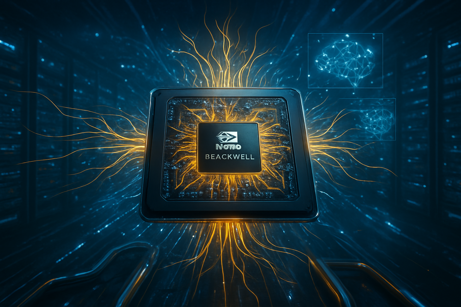
    The technical leap from the current HBM3E standard to HBM4 is the most significant in the history of the High Bandwidth Memory category. The most striking advancement is the doubling of the interface width from 1024-bit to 2048-bit per stack. This expanded "data highway" allows for a massive surge in throughput, with individual stacks now capable of exceeding 2.0 TB/s. For next-generation AI accelerators like the NVIDIA (NASDAQ: NVDA) Rubin architecture, this translates to an aggregate bandwidth of over 22 TB/s—nearly triple the performance of the groundbreaking Blackwell systems of 2024.

    Density has also seen a dramatic increase. The industry has standardized on 12-high (48GB) and 16-high (64GB) stacks. A single GPU equipped with eight 16-high HBM4 stacks can now access 512GB of high-speed VRAM on a single package. This massive capacity is made possible by the introduction of Hybrid Bonding and advanced Mass Reflow Molded Underfill (MR-MUF) techniques, allowing manufacturers to stack more layers without increasing the physical height of the chip.

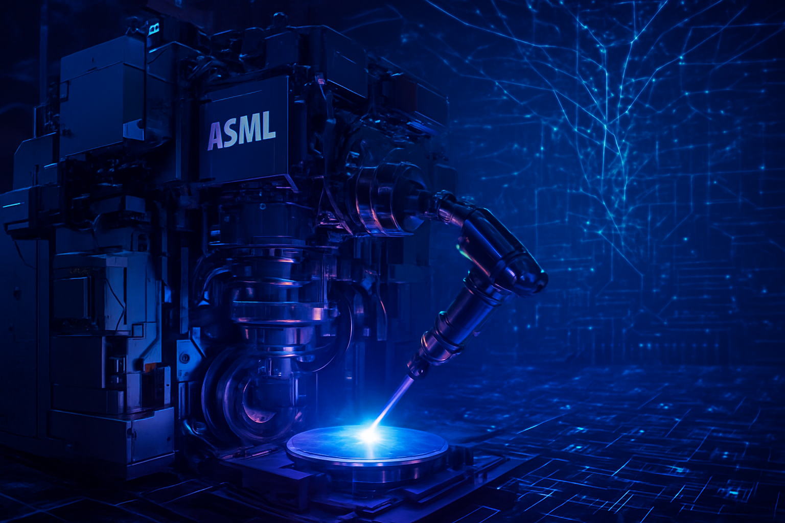
    Perhaps the most transformative change is the "Logic Die" revolution. Unlike previous generations that used passive base dies, HBM4 utilizes an active logic die manufactured on advanced foundry nodes. SK Hynix (KRX: 000660) and Micron Technology (NASDAQ: MU) have partnered with TSMC (NYSE: TSM) to produce these base dies using 5nm and 12nm processes, while Samsung Electronics (KRX: 005930) is utilizing its own 4nm foundry for a vertically integrated "turnkey" solution. This allows for Processing-in-Memory (PIM) capabilities, where basic data operations are performed within the memory stack itself, drastically reducing latency and power consumption.

    The HBM Gold Rush: Market Dominance and Strategic Alliances

    The commercial implications of HBM4 have created a "Sold Out" economy. Hyperscalers such as Microsoft (NASDAQ: MSFT), Meta (NASDAQ: META), and Alphabet (NASDAQ: GOOGL) have reportedly engaged in fierce bidding wars to secure 2026 allocations, leaving many smaller AI labs and startups facing lead times of 40 weeks or more. This supply crunch has solidified the dominance of the "Big Three" memory makers—SK Hynix, Samsung, and Micron—who are seeing record-breaking margins on HBM products that sell for nearly eight times the price of traditional DDR5 memory.

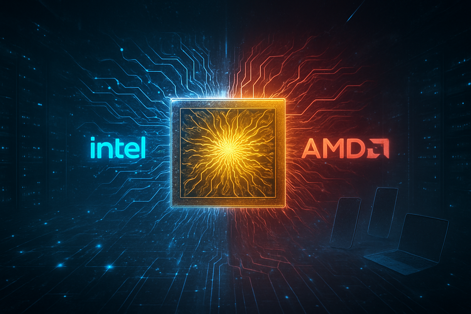
    In the chip sector, the rivalry between NVIDIA and AMD (NASDAQ: AMD) has reached a fever pitch. NVIDIA’s Vera Rubin (R200) platform, unveiled earlier this month at CES 2026, is the first to be built entirely around HBM4, positioning it as the premium choice for training trillion-parameter models. However, AMD is challenging this dominance with its Instinct MI400 series, which offers a 12-stack HBM4 configuration providing 432GB of capacity—purpose-built to compete in the burgeoning high-memory-inference market.

    The strategic landscape has also shifted toward a "Foundry-Memory Alliance" model. The partnership between SK Hynix and TSMC has proven formidable, leveraging TSMC’s CoWoS (Chip-on-Wafer-on-Substrate) packaging to maintain a slight edge in timing. Samsung, however, is betting on its ability to offer a "one-stop-shop" service, combining its memory, foundry, and packaging divisions to provide faster delivery cycles for custom HBM4 solutions. This vertical integration is designed to appeal to companies like Amazon (NASDAQ: AMZN) and Tesla (NASDAQ: TSLA), which are increasingly designing their own custom AI ASICs.

    Breaching the Memory Wall: Implications for the AI Landscape

    The arrival of HBM4 marks the end of the "Generative Era" and the beginning of the "Agentic Era." Current Large Language Models (LLMs) are often limited by their "KV Cache"—the working memory required to maintain context during long conversations. HBM4’s 512GB-per-GPU capacity allows AI agents to maintain context across millions of tokens, enabling them to handle multi-day workflows, such as autonomous software engineering or complex scientific research, without losing the thread of the project.

    Beyond capacity, HBM4 addresses the power efficiency crisis facing global data centers. By moving logic into the memory die, HBM4 reduces the distance data must travel, which significantly lowers the energy "tax" of moving bits. This is critical as the industry moves toward "World Models"—AI systems used in robotics and autonomous vehicles that must process massive streams of visual and sensory data in real-time. Without the bandwidth of HBM4, these models would be too slow or too power-hungry for edge deployment.

    However, the HBM4 boom has also exacerbated the "AI Divide." The 1:3 capacity penalty—where producing one HBM4 wafer consumes the manufacturing resources of three traditional DRAM wafers—has driven up the price of standard memory for consumer PCs and servers by over 60% in the last year. For AI startups, the high cost of HBM4-equipped hardware represents a significant barrier to entry, forcing many to pivot away from training foundation models toward optimizing "LLM-in-a-box" solutions that utilize HBM4's Processing-in-Memory features to run smaller models more efficiently.

    Looking Ahead: Toward HBM4E and Optical Interconnects

    As mass production of HBM4 ramps up throughout 2026, the industry is already looking toward the next horizon. Research into HBM4E (Extended) is well underway, with expectations for a late 2027 release. This future standard is expected to push capacities toward 1TB per stack and may introduce optical interconnects, using light instead of electricity to move data between the memory and the processor.

    The near-term focus, however, will be on the 16-high stack. While 12-high variants are shipping now, the 16-high HBM4 modules—the "holy grail" of current memory density—are targeted for Q3 2026 mass production. Achieving high yields on these complex 16-layer stacks remains the primary engineering challenge. Experts predict that the success of these modules will determine which companies can lead the race toward "Super-Intelligence" clusters, where tens of thousands of GPUs are interconnected to form a single, massive brain.

    A New Chapter in Computational History

    The rollout of HBM4 is more than a hardware refresh; it is the infrastructure foundation for the next decade of AI development. By doubling bandwidth and integrating logic directly into the memory stack, HBM4 has provided the "oxygen" required for the next generation of trillion-parameter models to breathe. Its significance in AI history will likely be viewed as the moment when the "Memory Wall" was finally breached, allowing silicon to move closer to the efficiency of the human brain.

    As we move through 2026, the key developments to watch will be Samsung’s mass production ramp-up in February and the first deployment of NVIDIA's Rubin clusters in mid-year. The global economy remains highly sensitive to the HBM supply chain, and any disruption in these critical memory stacks could ripple across the entire technology sector. For now, the HBM4 boom continues unabated, fueled by a world that has an insatiable hunger for memory and the intelligence it enables.


    This content is intended for informational purposes only and represents analysis of current AI developments.

    TokenRing AI delivers enterprise-grade solutions for multi-agent AI workflow orchestration, AI-powered development tools, and seamless remote collaboration platforms.
    For more information, visit https://www.tokenring.ai/.

  • The High-NA Era Arrives: How Intel’s $380M Lithography Bet is Redefining AI Silicon

    The High-NA Era Arrives: How Intel’s $380M Lithography Bet is Redefining AI Silicon

    The dawn of 2026 marks a historic inflection point in the semiconductor industry as the "mass production era" of High-Numerical Aperture (High-NA) Extreme Ultraviolet (EUV) lithography officially moves from laboratory speculation to the factory floor. Leading the charge, Intel (NASDAQ: INTC) has confirmed the completion of acceptance testing for its latest fleet of ASML (NASDAQ: ASML) Twinscan EXE:5200 systems, signaling the start of a multi-year transition toward the 1.4nm (14A) node. With each machine carrying a price tag exceeding $380 million, this development represents one of the most expensive and technically demanding gambles in industrial history, aimed squarely at sustaining the hardware requirements of the generative AI revolution.

    The significance of this transition cannot be overstated for the future of artificial intelligence. As transformer models grow in complexity, the demand for processors with higher transistor densities and lower power profiles has hit a physical wall with traditional EUV technology. By deploying High-NA tools, chipmakers are now able to print features with a resolution of approximately 8nm—nearly doubling the precision of previous generations. This shift is not merely an incremental upgrade; it is a fundamental reconfiguration of the economics of scaling, moving the industry toward a future where 1nm processors will eventually power the next decade of autonomous systems and trillion-parameter AI models.

    The Physics of 0.55 NA: A New Blueprint for Transistors

    At the heart of this revolution is ASML’s Twinscan EXE series, which increases the Numerical Aperture (NA) from 0.33 to 0.55. In practical terms, this allows the lithography machine to focus light more sharply, enabling the printing of significantly smaller features on a silicon wafer. While standard EUV tools required "multi-patterning"—a process of printing a single layer multiple times to achieve higher resolution—High-NA EUV enables single-exposure patterning for the most critical layers of a chip. This reduction in process complexity is expected to improve yields and shorten the time-to-market for cutting-edge AI accelerators, which have historically been plagued by the intricate manufacturing requirements of sub-3nm nodes.

    Technically, the transition to High-NA introduces an "anamorphic" optical system, which magnifies the X and Y axes differently. This design results in a "half-field" exposure, meaning the reticle size is effectively halved compared to standard EUV. To manufacture the massive dies required for high-end AI GPUs, such as those produced by NVIDIA (NASDAQ: NVDA), manufacturers must now employ "stitching" techniques to join two exposure fields into a single seamless pattern. This architectural shift has sparked intense discussion among AI researchers and hardware engineers, as it necessitates a move toward "chiplet" designs where multiple smaller dies are interconnected, rather than relying on a single monolithic slab of silicon.

    Intel’s primary vehicle for this technology is the 14A node, the world’s first process built from the ground up to be "High-NA native." Initial reports from Intel’s D1X facility in Oregon suggest that the EXE:5200B tools are achieving throughputs of over 220 wafers per hour, a critical metric for high-volume manufacturing. Industry experts note that while the $380 million capital expenditure per tool is staggering, the ability to eliminate multiple mask steps in the production cycle could eventually offset these costs, provided the volume of AI-specific silicon remains high.

    A High-Stakes Rivalry: Intel vs. Samsung and the "Lithography Divide"

    The deployment of High-NA EUV has created a strategic divide among the world’s three leading foundries. Intel’s aggressive "first-mover" advantage is a calculated attempt to regain process leadership after losing ground to competitors over the last decade. By securing the earliest shipments of the EXE:5200 series, Intel is positioning itself as the premier destination for custom AI silicon from tech giants like Microsoft (NASDAQ: MSFT) and Amazon (NASDAQ: AMZN), who are increasingly looking to design their own proprietary chips to optimize AI workloads.

    Samsung (KRX: 005930), meanwhile, has taken a dual-track approach. Having received its first High-NA units in 2025, the South Korean giant is integrating the technology into both its logic foundry and its advanced memory production. For Samsung, High-NA is essential for the development of HBM4 (High Bandwidth Memory), the specialized memory that feeds data to AI processors. The precision of High-NA is vital for the extreme vertical stacking required in next-generation HBM, making Samsung a formidable competitor in the AI hardware supply chain.

    In contrast, Taiwan Semiconductor Manufacturing Company (NYSE: TSM) has maintained a more conservative stance, opting to refine its existing 0.33 NA EUV processes for its 2nm (N2) node. This has created a "lithography divide" where Intel and Samsung are betting on the raw resolution of High-NA, while TSMC relies on its proven manufacturing excellence and cost-efficiency. The competitive implication is clear: if High-NA enables Intel to hit the 1.4nm milestone ahead of schedule, the balance of power in the global semiconductor market could shift back toward American and Korean soil for the first time in years.

    Moore’s Law and the Energy Crisis of AI

    The broader significance of the High-NA era lies in its role as a "lifeline" for Moore’s Law. For years, critics have predicted the end of transistor scaling, arguing that the heat and physical limitations of sub-atomically small components would eventually halt progress. High-NA EUV, combined with new transistor architectures like Gate-All-Around (GAA) and backside power delivery, provides a roadmap for another decade of scaling. This is particularly vital as the AI landscape shifts from "training" large models to "inference" at the edge, where energy efficiency is the primary constraint.

    Processors manufactured on the 1.4nm and 1nm nodes are expected to deliver up to a 30% reduction in power consumption compared to current 3nm chips. In an era where AI data centers are consuming an ever-larger share of the global power grid, these efficiency gains are not just an economic advantage—they are a geopolitical and environmental necessity. Without the scaling enabled by High-NA, the projected growth of generative AI would likely be throttled by the sheer energy requirements of the hardware needed to support it.

    However, the transition is not without its concerns. The extreme cost of High-NA tools threatens to centralize chip manufacturing even further, as only a handful of companies can afford the multi-billion dollar investment required to build a High-NA-capable "mega-fab." This concentration of advanced manufacturing capabilities raises questions about supply chain resilience and the accessibility of cutting-edge hardware for smaller AI startups. Furthermore, the technical challenges of "stitching" half-field exposures could lead to initial yield issues, potentially keeping prices high for the very AI chips the technology is meant to proliferate.

    The Road to 1.4nm and Beyond

    Looking ahead, the next 24 to 36 months will be focused on perfecting the transition from pilot production to High-Volume Manufacturing (HVM). Intel is targeting 2027 for the full commercialization of its 14A node, with Samsung likely following closely behind with its SF1.4 process. Beyond that, the industry is already eyeing the 1nm milestone—often referred to as the "Angstrom era"—where features will be measured at the scale of individual atoms.

    Future developments will likely involve the integration of High-NA with even more exotic materials and architectures. We can expect to see the rise of "2D semiconductors" and "carbon nanotube" components that take advantage of the extreme resolution provided by ASML’s optics. Additionally, as the physical limits of light-based lithography are reached, researchers are already exploring "Hyper-NA" systems with even higher apertures, though such technology remains in the early R&D phase.

    The immediate challenge remains the optimization of the photoresist chemicals and mask technology used within the High-NA machines. At such small scales, "stochastic effects"—random variations in the way light interacts with matter—become a major source of defects. Solving these material science puzzles will be the primary focus of the engineering community throughout 2026, as they strive to make the 1.4nm roadmap a reality for the mass market.

    A Watershed Moment for AI Infrastructure

    The arrival of the High-NA EUV mass production era is a watershed moment for the technology industry. It represents the successful navigation of one of the most difficult engineering hurdles in human history, ensuring that the physical hardware of the AI age can continue to evolve alongside the software. For Intel, it is a "do-or-die" moment to reclaim its crown; for Samsung, it is an opportunity to dominate both the brain (logic) and the memory of future AI systems.

    In summary, the transition to 0.55 NA lithography marks the end of the "low-resolution" era of semiconductor manufacturing. While the $380 million price tag per machine is a barrier to entry, the potential for 2.9x increases in transistor density offers a clear path toward the 1.4nm and 1nm chips that will define the late 2020s. The industry has effectively doubled down on hardware scaling to meet the insatiable appetite of AI.

    In the coming months, watchers should keep a close eye on the first "test chips" emerging from Intel’s 14A pilot lines. The success or failure of these early runs will dictate the pace of AI hardware advancement for the rest of the decade. As the first High-NA-powered processors begin to power the next generation of data centers, the true impact of this $380 million gamble will finally be revealed in the speed and efficiency of the AI models we use every day.


    This content is intended for informational purposes only and represents analysis of current AI developments.

    TokenRing AI delivers enterprise-grade solutions for multi-agent AI workflow orchestration, AI-powered development tools, and seamless remote collaboration platforms.
    For more information, visit https://www.tokenring.ai/.

  • Hell Freezes Over: Intel and AMD Unite to Save the x86 Empire from ARM’s Rising Tide

    Hell Freezes Over: Intel and AMD Unite to Save the x86 Empire from ARM’s Rising Tide

    In a move once considered unthinkable in the cutthroat world of semiconductor manufacturing, lifelong rivals Intel Corporation (NASDAQ: INTC) and Advanced Micro Devices, Inc. (NASDAQ: AMD) have solidified their "hell freezes over" alliance through the x86 Ecosystem Advisory Group (EAG). Formed in late 2024 and reaching a critical technical maturity in early 2026, this partnership marks a strategic pivot from decades of bitter competition to a unified front. The objective is clear: defend the aging but dominant x86 architecture against the relentless encroachment of ARM-based silicon, which has rapidly seized territory in both the high-end consumer laptop and hyper-scale data center markets.

    The significance of this development cannot be overstated. For forty years, Intel and AMD defined their success by their differences, often introducing incompatible instruction set extensions that forced software developers to choose sides or write complex, redundant code. Today, the x86 EAG—which includes a "founding board" of industry titans such as Microsoft Corporation (NASDAQ: MSFT), Alphabet Inc. (NASDAQ: GOOGL), Meta Platforms, Inc. (NASDAQ: META), and Broadcom Inc. (NASDAQ: AVGO)—represents a collective realization that the greatest threat to their future is no longer each other, but the energy-efficient, highly customizable architecture of the ARM ecosystem.

    Standardizing the Instruction Set: A Technical Renaissance

    The technical cornerstone of this alliance is a commitment to "consistent innovation," which aims to eliminate the fragmentation that has plagued the x86 instruction set architecture (ISA) for years. Leading into 2026, the group has finalized the specifications for AVX10, a unified vector instruction set that solves the long-standing "performance vs. efficiency" core dilemma. Unlike previous versions of AVX-512, which were often disabled on hybrid chips to maintain consistency across cores, AVX10 allows high-performance AI and scientific workloads to run seamlessly across all processor types, ensuring developers no longer have to navigate the "ISA tax" of targeting different hardware features within the same ecosystem.

    Beyond vector processing, the advisory group has introduced critical security and system modernizations. A standout feature is ChkTag (x86 Memory Tagging), a hardware-level security layer designed to combat buffer overflows and memory-corruption vulnerabilities. This is a direct response to ARM's Memory Tagging Extension (MTE), which has become a selling point for security-conscious enterprise clients. Additionally, the alliance has pushed forward the Flexible Return and Event Delivery (FRED) framework, which overhauls how CPUs handle interrupts—a legacy system that had not seen a major update since the 1980s. By streamlining these low-level operations, Intel and AMD are significantly reducing system latency and improving reliability in virtualized cloud environments.

    This unified approach differs fundamentally from the proprietary roadmaps of the past. Historically, Intel might introduce a feature like Intel AMX, only for it to remain unavailable on AMD hardware for years, leaving developers hesitant to adopt it. By folding initiatives like the "x86-S" simplified architecture into the EAG, the two giants are ensuring that major changes—such as the eventual removal of 16-bit and 32-bit legacy support—happen in lockstep. This coordinated evolution provides software vendors like Adobe or Epic Games with a stable, predictable target for the next decade of computing.

    Initial reactions from the technical community have been cautiously optimistic. Linus Torvalds, the creator of Linux and a technical advisor to the group, has noted that a more predictable x86 architecture simplifies kernel development immensely. However, industry experts point out that while standardizing the ISA is a massive step forward, the success of the EAG will ultimately depend on whether Intel and AMD can match the "performance-per-watt" benchmarks set by modern ARM designs. The era of brute-force clock speeds is over; the alliance must now prove that x86 can be as lean as it is powerful.

    The Competitive Battlefield: AI PCs and Cloud Sovereignty

    The competitive implications of this alliance ripple across the entire tech sector, particularly benefiting the "founding board" members who oversee the world’s largest software ecosystems. For Microsoft, a unified x86 roadmap ensures that Windows 11 and its successors can implement deep system-level optimizations that work across the vast majority of the PC market. Similarly, server-side giants like Dell Technologies Inc. (NYSE: DELL), HP Inc. (NYSE: HPQ), and Hewlett Packard Enterprise (NYSE: HPE) gain a more stable platform to market to enterprise clients who are increasingly tempted by the custom ARM chips of cloud providers.

    On the other side of the fence, the alliance is a direct challenge to the momentum of Apple Inc. (NASDAQ: AAPL) and Qualcomm Incorporated (NASDAQ: QCOM). Apple’s transition to its M-series silicon demonstrated that a tightly integrated, ARM-based stack could deliver industry-leading efficiency, while Qualcomm’s Snapdragon X series has brought competitive battery life to the Windows ecosystem. By modernizing x86, Intel and AMD are attempting to neutralize the "legacy bloat" argument that ARM proponents have used to win over OEMs. If the EAG succeeds in making x86 chips significantly more efficient, the strategic advantage currently held by ARM in the "always-connected" laptop space could evaporate.

    Hyperscalers like Amazon.com, Inc. (NASDAQ: AMZN) and Google stand in a complex position. While they sit on the EAG board, they also develop their own ARM-based processors like Graviton and Axion to reduce their reliance on third-party silicon. However, the x86 alliance provides these companies with a powerful hedge. By ensuring that x86 remains a viable, high-performance option for their data centers, they maintain leverage in price negotiations and ensure that the massive library of legacy enterprise software—which remains predominantly x86-based—continues to run optimally on their infrastructure.

    For the broader AI landscape, the alliance's focus on Advanced Matrix Extensions (ACE) provides a strategic advantage for on-device AI. As AI PCs become the standard in 2026, having a standardized instruction set for matrix multiplication ensures that AI software developers don't have to optimize their models separately for Intel Core Ultra and AMD Ryzen processors. This standardization could potentially disrupt the specialized NPU (Neural Processing Unit) market, as more AI tasks are efficiently offloaded to the standardized, high-performance CPU cores.

    A Strategic Pivot in Computing History

    The x86 Ecosystem Advisory Group arrives at a pivotal moment in the broader history of computing, echoing the seismic shifts seen during the transition from 32-bit to 64-bit architecture. For decades, the tech industry operated under the assumption that x86 was the permanent king of the desktop and server, while ARM was relegated to mobile devices. That boundary has been permanently shattered. The Intel-AMD alliance is a formal acknowledgment that the "Wintel" era of unchallenged dominance has ended, replaced by an era where architecture must justify its existence through efficiency and developer experience rather than just market inertia.

    This development is particularly significant in the context of the current AI revolution. The demand for massive compute power has traditionally favored x86’s raw performance, but the high energy costs of AI data centers have made ARM’s efficiency increasingly attractive. By collaborating to strip away legacy baggage and standardize AI-centric instructions, Intel and AMD are attempting to bridge the gap between "big iron" performance and modern efficiency requirements. It is a defensive maneuver, but one that is being executed with an aggressive focus on the future of the AI-native cloud.

    There are, however, potential concerns regarding the "duopoly" nature of this alliance. While the involvement of companies like Google and Meta is intended to provide a check on Intel and AMD’s power, some critics worry that a unified x86 standard could stifle niche architectural innovations. Comparisons are being drawn to the early days of the USB or PCIe standards—while they brought order to chaos, they also shifted the focus from radical breakthroughs to incremental, consensus-based updates.

    Ultimately, the EAG represents a shift from "competition through proprietary lock-in" to "competition through execution." By commoditizing the instruction set, Intel and AMD are betting that they can win based on who builds the best transistors, the most efficient power delivery systems, and the most advanced packaging, rather than who has the most unique (and frustrating) software extensions. It is a gamble that the x86 ecosystem is stronger than the sum of its rivals.

    Future Roadmaps: Scaling the AI Wall

    Looking ahead to the remainder of 2026 and into 2027, the first "EAG-compliant" silicon is expected to hit the market. These processors will be the true test of the alliance, featuring the finalized AVX10 and FRED standards out of the box. Near-term developments will likely focus on the "64-bit only" transition, with the group expected to release a formal timeline for the phasing out of native 16-bit and 32-bit hardware support. This will allow for even leaner chip designs, as silicon real estate currently dedicated to legacy compatibility is reclaimed for more cache or additional AI accelerators.

    In the long term, we can expect the x86 EAG to explore deeper integration with the software stack. There is significant speculation that the group is working on a "Universal Binary" format for Windows and Linux that would allow a single compiled file to run with maximum efficiency on any x86 chip from any vendor, effectively matching the seamless experience of the ARM-based macOS ecosystem. Challenges remain, particularly in ensuring that the many disparate members of the advisory group remain aligned as their individual business interests inevitably clash.

    Experts predict that the success of this alliance will dictate whether x86 remains the backbone of the enterprise world for the next thirty years or if it eventually becomes a legacy niche. If the EAG can successfully deliver on its promise of a modernized, unified, and efficient architecture, it will likely slow the migration to ARM significantly. However, if the group becomes bogged down in committee-level bureaucracy, the agility of the ARM ecosystem—and the rising challenge of the open-source RISC-V architecture—may find an even larger opening to exploit.

    Conclusion: The New Era of Unified Silicon

    The formation and technical progress of the x86 Ecosystem Advisory Group represent a watershed moment in the semiconductor industry. By uniting against a common threat, Intel and AMD have effectively ended a forty-year civil war to preserve the legacy and future of the architecture that powered the digital age. The key takeaways from this alliance are the standardization of AI and security instructions, the coordinated removal of legacy bloat, and the unprecedented collaboration between silicon designers and software giants to create a unified developer experience.

    As we look at the history of AI and computing, this alliance will likely be remembered as the moment when the "old guard" finally adapted to the realities of a post-mobile, AI-first world. The significance lies not just in the technical specifications, but in the cultural shift: the realization that in a world of custom silicon and specialized accelerators, the ecosystem is the ultimate product.

    In the coming weeks and months, industry watchers should look for the first third-party benchmarks of AVX10-enabled software and any announcements regarding the next wave of members joining the advisory group. As the first EAG-optimized servers begin to roll out to data centers in mid-2026, we will see the first real-world evidence of whether this "hell freezes over" pact is enough to keep the x86 crown from slipping.


    This content is intended for informational purposes only and represents analysis of current AI developments.

    TokenRing AI delivers enterprise-grade solutions for multi-agent AI workflow orchestration, AI-powered development tools, and seamless remote collaboration platforms.
    For more information, visit https://www.tokenring.ai/.

  • The 2nm Epoch: TSMC’s N2 Node Hits Mass Production as the Advanced AI Chip Race Intensifies

    The 2nm Epoch: TSMC’s N2 Node Hits Mass Production as the Advanced AI Chip Race Intensifies

    As of January 16, 2026, the global semiconductor landscape has officially entered the "2-nanometer era," marking the most significant architectural shift in silicon manufacturing in over a decade. Taiwan Semiconductor Manufacturing Company (TSMC) (NYSE: TSM) has confirmed that its N2 (2nm-class) technology node reached high-volume manufacturing (HVM) in late 2025 and is currently ramping up capacity at its state-of-the-art Fab 20 in Hsinchu and Fab 22 in Kaohsiung. This milestone represents a critical pivot point for the industry, as it marks TSMC’s transition away from the long-standing FinFET transistor structure to the revolutionary Gate-All-Around (GAA) nanosheet architecture.

    The immediate significance of this development cannot be overstated. As the backbone of the AI revolution, the N2 node is expected to power the next generation of high-performance computing (HPC) and mobile processors, offering the thermal efficiency and logic density required to sustain the massive growth in generative AI. With initial 2nm capacity for 2026 already reportedly fully booked, the launch of N2 solidifies TSMC’s position as the primary gatekeeper for the world’s most advanced artificial intelligence hardware.

    Transitioning to Nanosheets: The Technical Core of N2

    The N2 node is a technical tour de force, centered on the shift from FinFET to Gate-All-Around (GAA) nanosheet transistors. In a FinFET structure, the gate wraps around three sides of the channel; in the new N2 nanosheet architecture, the gate surrounds the channel on all four sides. This provides superior electrostatic control, which is essential for reducing "current leakage"—a major hurdle that plagued previous nodes at 3nm. By better managing the flow of electrons, TSMC has achieved a performance boost of 10–15% at the same power level, or a power reduction of 25–30% at the same speed compared to the existing N3E (3nm) node.

    Beyond the transistor change, N2 introduces "Super-High-Performance Metal-Insulator-Metal" (SHPMIM) capacitors. These capacitors double the capacitance density while halving resistance, ensuring that power delivery remains stable even during the intense, high-frequency bursts of activity characteristic of AI training and inference. While TSMC has opted to delay "backside power delivery" until the N2P and A16 nodes later in 2026 and 2027, the current N2 iteration offers a 15% increase in mixed design density, making it the most compact and efficient platform for complex AI system-on-chips (SoCs).

    The industry reaction has been one of cautious optimism. While TSMC's reported initial yields of 65–75% are considered high for a new architecture, the complexity of the GAA transition has led to a 3–5% price hike for 2nm wafers. Experts from the semiconductor research community note that TSMC’s "incremental" approach—stabilizing the nanosheet architecture before adding backside power—is a strategic move to ensure supply chain reliability, even as competitors like Intel (NASDAQ: INTC) push more aggressive technical roadmaps.

    The 2nm Customer Race: Apple, Nvidia, and the Competitive Landscape

    Apple (NASDAQ: AAPL) has once again secured its position as TSMC’s anchor tenant, reportedly claiming over 50% of the initial N2 capacity. This ensures that the upcoming "A20 Pro" chip, expected to debut in the iPhone 18 series in late 2026, will be the first consumer-facing 2nm processor. Beyond mobile, Apple’s M6 series for Mac and iPad is being designed on N2 to maintain a battery-life advantage in an increasingly competitive "AI PC" market. By locking in this capacity, Apple effectively prevents rivals from accessing the most efficient silicon for another year.

    For Nvidia (NASDAQ: NVDA), the stakes are even higher. While the company has utilized custom 4nm and 3nm nodes for its Blackwell and Rubin architectures, the upcoming "Feynman" architecture is expected to leverage the 2nm class to drive the next leap in data center GPU performance. However, there is growing speculation that Nvidia may opt for the enhanced N2P or the 1.6nm A16 node to take advantage of backside power delivery, which is more critical for the massive power draws of AI training clusters.

    The competitive landscape is more contested than in previous years. Intel (NASDAQ: INTC) recently achieved a major milestone with its 18A node, launching the "Panther Lake" processors at CES 2026. By integrating its "PowerVia" backside power technology ahead of TSMC, Intel currently claims a performance-per-watt lead in certain mobile segments. Meanwhile, Samsung Electronics (KRX: 005930) is shipping its 2nm Exynos 2600 for the Galaxy S26. Despite having more experience with GAA (which it introduced at 3nm), Samsung continues to face yield struggles, reportedly stuck at approximately 50%, making it difficult to lure "whale" customers away from the TSMC ecosystem.

    Global Significance and the Energy Imperative

    The launch of N2 fits into a broader trend where AI compute demand is outstripping energy availability. As data centers consume a growing percentage of the global power supply, the 25–30% efficiency gain offered by the 2nm node is no longer just a luxury—it is a requirement for the expansion of AI services. If the industry cannot find ways to reduce the power-per-operation, the environmental and financial costs of scaling models like GPT-5 or its successors will become prohibitive.

    However, the shift to 2nm also highlights deepening geopolitical concerns. With TSMC’s primary 2nm production remaining in Taiwan, the "silicon shield" becomes even more critical to global economic stability. This has spurred a massive push for domestic manufacturing, though TSMC’s Arizona and Japan plants are currently trailing the Taiwan-based "mother fabs" by at least one full generation. The high cost of 2nm development also risks a widening "compute divide," where only the largest tech giants can afford the billions in R&D and manufacturing costs required to utilize the leading-edge nodes.

    Comparatively, the transition to 2nm is as significant as the move to 3D transistors (FinFET) in 2011. It represents the end of the "classical" era of semiconductor scaling and the beginning of the "architectural" era, where performance gains are driven as much by how the transistor is built and powered as they are by how small it is.

    The Road Ahead: N2P, A16, and the 1nm Horizon

    Looking toward the near term, TSMC has already signaled that N2 is merely the first step in a multi-year roadmap. By late 2026, the company expects to introduce N2P, which will finally integrate "Super Power Rail" (backside power delivery). This will be followed closely by the A16 node, representing the 1.6nm class, which will introduce even more exotic materials and packaging techniques like CoWoS (Chip on Wafer on Substrate) to handle the extreme connectivity requirements of future AI clusters.

    The primary challenges ahead involve the "economic limit" of Moore's Law. As wafer prices increase, software optimization and custom silicon (ASICs) will become more important than ever. Experts predict that we will see a surge in "domain-specific" architectures, where chips are designed for a single specific AI task—such as large language model inference—to maximize the efficiency of the expensive 2nm silicon.

    Challenges also remain in the lithography space. As the industry moves toward "High-NA" EUV (Extreme Ultraviolet) machines, the costs of the equipment are skyrocketing. TSMC’s ability to maintain high yields while managing these astronomical costs will determine whether 2nm remains the standard for the next five years or if a new competitor can finally disrupt the status quo.

    Summary of the 2nm Landscape

    As we move through 2026, TSMC’s N2 node stands as the gold standard for semiconductor manufacturing. By successfully transitioning to GAA nanosheet transistors and maintaining superior yields compared to Samsung and Intel, TSMC has ensured that the next generation of AI breakthroughs will be built on its foundation. While Intel’s 18A presents a legitimate technical threat with its early adoption of backside power, TSMC’s massive ecosystem and reliability continue to make it the preferred partner for industry leaders like Apple and Nvidia.

    The significance of this development in AI history is profound; the N2 node provides the physical substrate necessary for the next leap in machine intelligence. In the coming months, the industry will be watching for the first third-party benchmarks of 2nm chips and the progress of TSMC’s N2P ramp-up. The race for silicon supremacy has never been tighter, and the stakes—powering the future of human intelligence—have never been higher.


    This content is intended for informational purposes only and represents analysis of current AI developments.

    TokenRing AI delivers enterprise-grade solutions for multi-agent AI workflow orchestration, AI-powered development tools, and seamless remote collaboration platforms.
    For more information, visit https://www.tokenring.ai/.

  • The Silicon Brain: NVIDIA’s BlueField-4 and the Dawn of the Agentic AI Chip Era

    The Silicon Brain: NVIDIA’s BlueField-4 and the Dawn of the Agentic AI Chip Era

    In a move that signals the definitive end of the "chatbot era" and the beginning of the "autonomous agent era," NVIDIA (NASDAQ: NVDA) has officially unveiled its new BlueField-4 Data Processing Unit (DPU) and the underlying Vera Rubin architecture. Announced this month at CES 2026, these developments represent a radical shift in how silicon is designed, moving away from raw mathematical throughput and toward hardware capable of managing the complex, multi-step reasoning cycles and massive "stateful" memory required by next-generation AI agents.

    The significance of this announcement cannot be overstated: for the first time, the industry is seeing silicon specifically engineered to solve the "Context Wall"—the primary physical bottleneck preventing AI from acting as a truly autonomous digital employee. While previous GPU generations focused on training massive models, BlueField-4 and the Rubin platform are built for the execution of agentic workflows, where AI doesn't just respond to prompts but orchestrates its own sub-tasks, maintains long-term memory, and reasons across millions of tokens of context in real-time.

    The Architecture of Autonomy: Inside BlueField-4

    Technical specifications for the BlueField-4 reveal a massive leap in orchestrational power. Boasting 64 Arm Neoverse V2 cores—a six-fold increase over the previous BlueField-3—and a blistering 800 Gb/s throughput via integrated ConnectX-9 networking, the chip is designed to act as the "nervous system" of the Vera Rubin platform. Unlike standard processors, BlueField-4 introduces the Inference Context Memory Storage (ICMS) platform. This creates a new "G3.5" storage tier—a high-speed, Ethernet-attached flash layer that sits between the GPU’s ultra-fast High Bandwidth Memory (HBM) and traditional data center storage.

    This architectural shift is critical for "long-context reasoning." In agentic AI, the system must maintain a Key-Value (KV) cache—essentially the "active memory" of every interaction and data point an agent encounters during a long-running task. Previously, this cache would quickly overwhelm a GPU's memory, causing "context collapse." BlueField-4 offloads and manages this memory management at ultra-low latency, effectively allowing agents to "remember" thousands of pages of history and complex goals without stalling the primary compute units. This approach differs from previous technologies by treating the entire data center fabric, rather than a single chip, as the fundamental unit of compute.

    Initial reactions from the AI research community have been electric. "We are moving from one-shot inference to reasoning loops," noted Simon Robinson, an analyst at Omdia. Experts highlight that while startups like Etched have focused on "burning" Transformer models into specialized ASICs for raw speed, and Groq (the current leader in low-latency Language Processing Units) has prioritized "Speed of Thought," NVIDIA’s BlueField-4 offers the infrastructure necessary for these agents to work in massive, coordinated swarms. The industry consensus is that 2026 will be the year of high-utility inference, where the hardware finally catches up to the demands of autonomous software.

    Market Wars: The Integrated vs. The Open

    NVIDIA’s announcement has effectively divided the high-end AI market into two distinct camps. By integrating the Vera CPU, Rubin GPU, and BlueField-4 DPU into a singular, tightly coupled ecosystem, NVIDIA (NASDAQ: NVDA) is doubling down on its "Apple-like" strategy of vertical integration. This positioning grants the company a massive strategic advantage in the enterprise sector, where companies are desperate for "turnkey" agentic solutions. However, this move has also galvanized the competition.

    Advanced Micro Devices (NASDAQ: AMD) responded at CES with its own "Helios" platform, featuring the MI455X GPU. Boasting 432GB of HBM4 memory—the largest in the industry—AMD is positioning itself as the "Android" of the AI world. By leading the Ultra Accelerator Link (UALink) consortium, AMD is championing an open, modular architecture that allows hyperscalers like Google and Amazon to mix and match hardware. This competitive dynamic is likely to disrupt existing product cycles, as customers must now choose between NVIDIA’s optimized, closed-loop performance and the flexibility of the AMD-led open standard.

    Startups like Etched and Groq also face a new reality. While their specialized silicon offers superior performance for specific tasks, NVIDIA's move to integrate agentic management directly into the data center fabric makes it harder for specialized ASICs to gain a foothold in general-purpose data centers. Major AI labs, such as OpenAI and Anthropic, stand to benefit most from this development, as the drop in "token-per-task" costs—projected to be up to 10x lower with BlueField-4—will finally make the mass deployment of autonomous agents economically viable.

    Beyond the Chatbot: The Broader AI Landscape

    The shift toward agentic silicon marks a significant milestone in AI history, comparable to the original "Transformer" breakthrough of 2017. We are moving away from "Generative AI"—which focuses on creating content—toward "Agentic AI," which focuses on achieving outcomes. This evolution fits into the broader trend of "Physical AI" and "Sovereign AI," where nations and corporations seek to build autonomous systems that can manage power grids, optimize supply chains, and conduct scientific research with minimal human intervention.

    However, the rise of chips designed for autonomous decision-making brings significant concerns. As hardware becomes more efficient at running long-horizon reasoning, the "black box" problem of AI transparency becomes more acute. If an agentic system makes a series of autonomous decisions over several hours of compute time, auditing that decision-making path becomes a Herculean task for human overseers. Furthermore, the power consumption required to maintain the "G3.5" memory tier at a global scale remains a looming environmental challenge, even with the efficiency gains of the 3nm and 2nm process nodes.

    Compared to previous milestones, the BlueField-4 era represents the "industrialization" of AI reasoning. Just as the steam engine required specialized infrastructure to become a global force, agentic AI requires this new silicon "nervous system" to move out of the lab and into the foundation of the global economy. The transition from "thinking" chips to "acting" chips is perhaps the most significant hardware pivot of the decade.

    The Horizon: What Comes After Rubin?

    Looking ahead, the roadmap for agentic silicon is moving toward even tighter integration. Near-term developments will likely focus on "Agentic Processing Units" (APUs)—a rumored 2027 product category that would see CPU, GPU, and DPU functions merged onto a single massive "system-on-a-chip" (SoC) for edge-based autonomy. We can expect to see these chips integrated into sophisticated robotics and autonomous vehicles, allowing for complex decision-making without a constant connection to the cloud.

    The challenges remaining are largely centered on memory bandwidth and heat dissipation. As agents become more complex, the demand for HBM4 and HBM5 will likely outstrip supply well into 2027. Experts predict that the next "frontier" will be the development of neuromorphic-inspired memory architectures that mimic the human brain's ability to store and retrieve information with almost zero energy cost. Until then, the industry will be focused on mastering the "Vera Rubin" platform and proving that these agents can deliver a clear Return on Investment (ROI) for the enterprises currently spending billions on infrastructure.

    A New Chapter in Silicon History

    NVIDIA’s BlueField-4 and the Rubin architecture represent more than just a faster chip; they represent a fundamental re-definition of what a "computer" is. In the agentic era, the computer is no longer a device that waits for instructions; it is a system that understands context, remembers history, and pursues goals. The pivot from training to stateful, long-context reasoning is the final piece of the puzzle required to make AI agents a ubiquitous part of daily life.

    As we look toward the second half of 2026, the key metric for success will no longer be TFLOPS (Teraflops), but "Tokens per Task" and "Reasoning Steps per Watt." The arrival of BlueField-4 has set a high bar for the rest of the industry, and the coming months will likely see a flurry of counter-announcements as the "Silicon Wars" enter their most intense phase yet. For now, the message from the hardware world is clear: the agents are coming, and the silicon to power them is finally ready.


    This content is intended for informational purposes only and represents analysis of current AI developments.

    TokenRing AI delivers enterprise-grade solutions for multi-agent AI workflow orchestration, AI-powered development tools, and seamless remote collaboration platforms.
    For more information, visit https://www.tokenring.ai/.

  • The End of Air Cooling: TSMC and NVIDIA Pivot to Direct-to-Silicon Microfluidics for 2,000W AI “Superchips”

    The End of Air Cooling: TSMC and NVIDIA Pivot to Direct-to-Silicon Microfluidics for 2,000W AI “Superchips”

    As the artificial intelligence revolution accelerates into 2026, the industry has officially collided with a physical barrier: the "Thermal Wall." With the latest generation of AI accelerators now demanding upwards of 1,000 to 2,300 watts of power, traditional air cooling and even standard liquid-cooled cold plates have reached their limits. In a landmark shift for semiconductor architecture, NVIDIA (NASDAQ: NVDA) and Taiwan Semiconductor Manufacturing Company (NYSE: TSM) have moved to integrate liquid cooling channels directly into the silicon and packaging of their next-generation Blackwell and Rubin series chips.

    This transition marks one of the most significant architectural pivots in the history of computing. By etching microfluidic channels directly into the chip's backside or integrated heat spreaders, engineers are now bringing coolant within microns of the active transistors. This "Direct-to-Silicon" approach is no longer an experimental luxury but a functional necessity for the Rubin R100 GPUs, which were recently unveiled at CES 2026 as the first mass-market processors to cross the 2,000W threshold.

    Breaking the 2,000W Barrier: The Technical Leap to Microfluidics

    The technical specifications of the new Rubin series represent a staggering leap from the previous Blackwell architecture. While the Blackwell B200 and GB200 series (released in 2024-2025) pushed thermal design power (TDP) to the 1,200W range using advanced copper cold plates, the Rubin architecture pushes this as high as 2,300W per GPU. At this density, the bottleneck is no longer the liquid loop itself, but the "Thermal Interface Material" (TIM)—the microscopic layers of paste and solder that sit between the chip and its cooler. To solve this, TSMC has deployed its Silicon-Integrated Micro Cooler (IMC-Si) technology, effectively turning the chip's packaging into a high-performance heat exchanger.

    This "water-in-wafer" strategy utilizes microchannels ranging from 30 to 150 microns in width, etched directly into the silicon or the package lid. By circulating deionized water or dielectric fluids through these channels, TSMC has achieved a thermal resistance as low as 0.055 °C/W. This is a 15% improvement over the best external cold plate solutions and allows for the dissipation of heat that would literally melt a standard processor in seconds. Unlike previous approaches where cooling was a secondary component bolted onto a finished chip, these microchannels are now a fundamental part of the CoWoS (Chip-on-Wafer-on-Substrate) packaging process, ensuring a hermetic seal and zero-leak reliability.

    The industry has also seen the rise of the Microchannel Lid (MCL), a hybrid technology adopted for the initial Rubin R100 rollout. Developed in partnership with specialists like Jentech Precision (TPE: 3653), the MCL integrates cooling channels into the stiffener of the chip package itself. This eliminates the "TIM2" layer, a major heat-transfer bottleneck in earlier designs. Industry experts note that this shift has transformed the bill of materials for AI servers; the cooling system, once a negligible cost, now represents a significant portion of the total hardware investment, with the average selling price of high-end lids increasing nearly tenfold.

    The Infrastructure Upheaval: Winners and Losers in the Cooling Wars

    The shift to direct-to-silicon cooling is fundamentally reorganizing the AI supply chain. Traditional air-cooling specialists are being sidelined as data center operators scramble to retrofit facilities for 100% liquid-cooled racks. Companies like Vertiv (NYSE: VRT) and Schneider Electric (EPA: SU) have become central players in the AI ecosystem, providing the Coolant Distribution Units (CDUs) and secondary loops required to feed the ravenous microchannels of the Rubin series. Supermicro (NASDAQ: SMCI) has also solidified its lead by offering "Plug-and-Play" liquid-cooled clusters that can handle the 120kW+ per rack loads generated by the GB200 and Rubin NVL72 configurations.

    Strategically, this development grants NVIDIA a significant moat against competitors who are slower to adopt integrated cooling. By co-designing the silicon and the thermal management system with TSMC, NVIDIA can pack more transistors and drive higher clock speeds than would be possible with traditional cooling. Competitors like AMD (NASDAQ: AMD) and Intel (NASDAQ: INTC) are also pivoting; AMD’s latest MI400 series is rumored to follow a similar path, but NVIDIA’s early vertical integration with the cooling supply chain gives them a clear time-to-market advantage.

    Furthermore, this shift is creating a new class of "Super-Scale" data centers. Older facilities, limited by floor weight and power density, are finding it nearly impossible to host the latest AI clusters. This has sparked a surge in new construction specifically designed for liquid-to-the-chip architecture. Startups specializing in exotic cooling, such as JetCool and Corintis, are also seeing record venture capital interest as tech giants look for even more efficient ways to manage the heat of future 3,000W+ "Superchips."

    A New Era of High-Performance Sustainability

    The move to integrated liquid cooling is not just about performance; it is also a critical response to the soaring energy demands of AI. While it may seem counterintuitive that a 2,000W chip is "sustainable," the efficiency gains at the system level are profound. Traditional air-cooled data centers often spend 30% to 40% of their total energy just on fans and air conditioning. In contrast, the direct-to-silicon liquid cooling systems of 2026 can drive a Power Usage Effectiveness (PUE) rating as low as 1.07, meaning almost all the energy entering the building is going directly into computation rather than cooling.

    This milestone mirrors previous breakthroughs in high-performance computing (HPC), where liquid cooling was the standard for top-tier supercomputers. However, the scale is vastly different today. What was once reserved for a handful of government labs is now the standard for the entire enterprise AI market. The broader significance lies in the decoupling of power density from physical space; by moving heat more efficiently, the industry can continue to follow a "Modified Moore's Law" where compute density increases even as transistors hit their physical size limits.

    However, the move is not without concerns. The complexity of these systems introduces new points of failure. A single leak in a microchannel loop could destroy a multi-million dollar server rack. This has led to a boom in "smart monitoring" AI, where secondary neural networks are used solely to predict and prevent thermal anomalies or fluid pressure drops within the chip's cooling channels. The industry is currently debating the long-term reliability of these systems over a 5-to-10-year data center lifecycle.

    The Road to Wafer-Scale Cooling and 3,600W Chips

    Looking ahead, the roadmap for 2027 and beyond points toward even more radical cooling integration. TSMC has already previewed its System-on-Wafer-X (SoW-X) technology, which aims to integrate up to 16 compute dies and 80 HBM4 memory stacks on a single 300mm wafer. Such an entity would generate a staggering 17,000 watts of heat per wafer-module. Managing this will require "Wafer-Scale Cooling," where the entire substrate is essentially a giant heat sink with embedded fluid jets.

    Experts predict that the upcoming "Rubin Ultra" series, expected in 2027, will likely push TDP to 3,600W. To support this, the industry may move beyond water to advanced dielectric fluids or even two-phase immersion cooling where the fluid boils and condenses directly on the silicon surface. The challenge remains the integration of these systems into standard data center workflows, as the transition from "plumber-less" air cooling to high-pressure fluid management requires a total re-skilling of the data center workforce.

    The next few months will be crucial as the first Rubin-based clusters begin their global deployments. Watch for announcements regarding "Green AI" certifications, as the ability to utilize the waste heat from these liquid-cooled chips for district heating or industrial processes becomes a major selling point for local governments and environmental regulators.

    Final Assessment: Silicon and Water as One

    The transition to Direct-to-Silicon liquid cooling is more than a technical upgrade; it is the moment the semiconductor industry accepted that silicon and water must exist in a delicate, integrated dance to keep the AI dream alive. As we move through 2026, the era of the noisy, air-conditioned data center is rapidly fading, replaced by the quiet hum of high-pressure fluid loops and the high-efficiency "Power Racks" that house them.

    This development will be remembered as the point where thermal management became just as important as logic design. The success of NVIDIA's Rubin series and TSMC's 3DFabric platforms has proven that the "thermal wall" can be overcome, but only by fundamentally rethinking the physical structure of a processor. In the coming weeks, keep a close eye on the quarterly earnings of thermal suppliers and data center REITs, as they will be the primary indicators of how fast this liquid-cooled future is arriving.


    This content is intended for informational purposes only and represents analysis of current AI developments.

    TokenRing AI delivers enterprise-grade solutions for multi-agent AI workflow orchestration, AI-powered development tools, and seamless remote collaboration platforms.
    For more information, visit https://www.tokenring.ai/.

  • The Angstrom Frontier: TSMC and Intel Reveal 1.4nm Roadmaps to Power the Next Decade of AI

    The Angstrom Frontier: TSMC and Intel Reveal 1.4nm Roadmaps to Power the Next Decade of AI

    As of January 13, 2026, the global semiconductor industry has officially entered a high-stakes sprint toward the "Angstrom Era," a move that promises to redefine the limits of silicon physics. Within the last several months, the industry's two primary titans, Taiwan Semiconductor Manufacturing Company Limited (NYSE: TSM) and Intel Corporation (NASDAQ: INTC), have solidified their long-term roadmaps for the 1.4nm node—designated as A14 and Intel 14A, respectively. This shift is not merely an incremental update; it represents a desperate race to provide the computational density required by upcoming generative AI models that are expected to be orders of magnitude larger than those of 2025.

    The move to 1.4nm, targeted for high-volume manufacturing between late 2027 and 2028, marks the point where the semiconductor industry must confront the "1nm wall." At these scales, the thickness of transistor gates is measured in just a handful of atoms, and traditional manufacturing techniques fail to prevent electrons from "leaking" through supposedly solid barriers. The significance of this milestone cannot be overstated: the success of these 1.4nm nodes will determine whether the current AI boom can sustain its exponential growth or if it will be throttled by a literal "power wall" in global data centers.

    Engineering the Impossible: The Physics of 14 Angstroms

    The transition to 1.4nm requires a fundamental reimagining of transistor architecture and lithography. While the previous 2nm nodes introduced Gate-All-Around (GAA) transistors—where the gate surrounds the channel on all four sides to minimize current leakage—the 1.4nm era refines this with second-generation GAA designs. Intel’s "14A" node will utilize its evolved RibbonFET 2 architecture, while TSMC’s "A14" will deploy its own advanced nanosheet technology. The goal is to achieve a 15–20% performance-per-watt improvement over the 2nm generation, a necessity as AI chips like those from NVIDIA Corporation (NASDAQ: NVDA) push thermal envelopes to their breaking points.

    A major technical schism has emerged regarding High-Numerical Aperture (High-NA) Extreme Ultraviolet (EUV) lithography. Intel has taken a "vanguard" approach, becoming the first to install ASML Holding’s (NASDAQ: ASML) massive $400 million High-NA machines. These tools allow for much finer resolution, enabling Intel to print 1.4nm features in a single pass. Conversely, TSMC has opted for a "fast-follower" strategy, announcing it will initially bypass High-NA EUV for its A14 node in favor of advanced multi-patterning using existing Low-NA EUV tools. TSMC argues that its mature toolset will offer higher yields and lower costs for customers like Apple Inc. (NASDAQ: AAPL), even if the process is more complex to execute.

    Beyond lithography, both companies are tackling the "interconnect bottleneck." As wires shrink to atomic widths, traditional copper becomes highly resistive, generating excessive heat. To combat this, 1.4nm nodes are expected to incorporate exotic materials such as Ruthenium or Cobalt-Ruthenium binary liners. Furthermore, "Backside Power Delivery"—a technique that moves the power-delivery circuitry to the bottom of the silicon wafer to free up the top for signal routing—will become standard. Intel’s PowerDirect and TSMC’s Super Power Rail are the primary weapons in this fight against voltage sag and thermal throttling.

    The Foundry War: TSMC's Dominance vs. Intel's Ambition

    The 1.4nm roadmap has ignited a fierce strategic battle for market share in the AI accelerator space. For years, TSMC has held a near-monopoly on high-end AI silicon, but Intel’s aggressive "five nodes in four years" strategy has finally brought it within striking distance. Intel is marketing its 14A node as part of its "AI System Foundry" model, which integrates advanced 1.4nm logic with proprietary 3D packaging technologies like Foveros. By offering a "one-stop-shop" that includes the latest High-NA manufacturing and cutting-edge packaging, Intel hopes to lure major clients away from the Taiwanese giant.

    For NVIDIA Corporation and Advanced Micro Devices, Inc. (NASDAQ: AMD), the 1.4nm era offers a crucial second-sourcing opportunity. Industry insiders suggest that NVIDIA is closely evaluating Intel’s 14A process for its post-2027 "Feynman" architecture as a hedge against geopolitical instability in the Taiwan Strait and capacity constraints at TSMC. If Intel can prove its 1.4nm yields are stable, it could break TSMC’s stranglehold on the AI GPU market, leading to a more competitive pricing environment for the hardware that powers the world's LLMs.

    TSMC, however, remains the incumbent favorite due to its peerless execution history. Its "NanoFlex Pro" technology, which allows chip designers to mix different transistor heights on a single die, offers a level of customization that is highly attractive to hyper-scalers like Amazon and Google who are designing their own bespoke AI chips. By focusing on manufacturing reliability and yield over "first-to-market" bragging rights with High-NA EUV, TSMC aims to remain the primary foundry for the world's most valuable technology companies.

    Scaling Laws and the AI Power Wall

    The shift to 1.4nm fits into a broader narrative of "AI Scaling Laws," which suggest that increasing the amount of compute and data leads to predictable improvements in model intelligence. However, these laws are currently hitting a physical barrier: the "Power Wall." Current data centers are reaching the limits of available electrical grids. The 30% power reduction promised by the A14 and 14A nodes is seen by many researchers as the only way to keep scaling model parameters without requiring dedicated nuclear power plants for every new training cluster.

    There are significant concerns, however, regarding Quantum Tunneling. At 1.4nm, the insulating layers within a transistor are so thin that electrons can simply "jump" across them due to quantum effects, leading to massive energy waste. While GAA and new materials mitigate this, some physicists argue we are approaching the "Red Line" of silicon-based computing. This has led to comparisons with the end of the "Dennard Scaling" era in the mid-2000s; just as we moved to multi-core processors then, the 1.4nm era may force a shift toward entirely new computing paradigms, such as optical computing or neuromorphic chips.

    Despite these hurdles, the industry's consensus is that the Angstrom Era is the final frontier for traditional silicon. The 1.4nm milestone is viewed with the same reverence as the 7nm "breakthrough" of 2018, which enabled the current generation of mobile and cloud computing. It represents a "survival node"—if the industry cannot successfully navigate the physics of 14 Angstroms, the pace of AI advancement could decelerate for the first time in a decade.

    Beyond 1.4nm: What Lies on the Horizon?

    As we look past 2028, the roadmap becomes increasingly speculative but no less ambitious. Both TSMC and Intel have already begun early research into the 1nm (10 Angstrom) node, which is expected to arrive around 2030. These future developments will likely require the transition from silicon to 2D materials like molybdenum disulfide (MoS2) or carbon nanotubes, which offer better electron mobility at atomic thicknesses. The packaging of these chips will also evolve, moving toward "monolithic 3D integration" where layers of logic are grown directly on top of each other.

    In the near term, the industry will be watching the "risk production" phases of 1.4nm in late 2026 and early 2027. The first indicators of success will not be raw speed, but rather the defect density and yield rates of these incredibly complex chips. Experts predict that the first 1.4nm chips to hit the market will likely be high-end mobile processors for a future "iPhone 19" or enterprise-grade AI accelerators designed for the training of "GPT-6" class models.

    The primary challenge remains economic. With High-NA EUV machines costing nearly half a billion dollars each, the cost of designing a single 1.4nm chip is projected to exceed $1 billion. This suggests a future where only a handful of the world's largest companies can afford to play at the leading edge, potentially centralizing AI power even further among a small group of tech titans.

    Closing the Angstrom Gap

    The emergence of the 1.4nm roadmap signals that the semiconductor industry is unwilling to let the laws of physics stall the momentum of artificial intelligence. By committing to the "Angstrom Era," TSMC and Intel are placing a multi-billion dollar bet that they can engineer their way through quantum-scale barriers. The key takeaways are clear: the next three years will be defined by a transition to 1.4nm, the adoption of High-NA EUV, and a shift toward backside power delivery.

    In the history of AI, this development will likely be remembered as the moment when hardware became the ultimate arbiter of intelligence. As we move closer to the 2027–2028 window, the industry will be watching for the first "silicon success" reports from Intel's Oregon facility and TSMC's Hsinchu Science Park. The long-term impact will be a world where AI is more pervasive, but also more dependent than ever on a fragile and incredibly expensive supply chain of atomic-scale machines.


    This content is intended for informational purposes only and represents analysis of current AI developments.

    TokenRing AI delivers enterprise-grade solutions for multi-agent AI workflow orchestration, AI-powered development tools, and seamless remote collaboration platforms.
    For more information, visit https://www.tokenring.ai/.

  • Samsung’s SF2 Gamble: 2nm Exynos 2600 Challenges TSMC’s Dominance

    Samsung’s SF2 Gamble: 2nm Exynos 2600 Challenges TSMC’s Dominance

    As the calendar turns to early 2026, the global semiconductor landscape has reached a pivotal inflection point with the official arrival of the 2nm era. Samsung Electronics (KRX:005930) has formally announced the mass production of its SF2 (2nm) process, a technological milestone aimed squarely at reclaiming the manufacturing crown from its primary rival, Taiwan Semiconductor Manufacturing Company (NYSE:TSM). The centerpiece of this rollout is the Exynos 2600, a next-generation mobile processor codenamed "Ulysses," which is set to power the upcoming Galaxy S26 series.

    This development is more than a routine hardware refresh; it represents Samsung’s strategic "all-in" bet on Gate-All-Around (GAA) transistor architecture. By integrating the SF2 node into its flagship consumer devices, Samsung is attempting to prove that its third-generation Multi-Bridge Channel FET (MBCFET) technology can finally match or exceed the stability and performance of TSMC’s 2nm offerings. The immediate significance lies in the Exynos 2600’s ability to handle the massive compute demands of on-device generative AI, which has become the primary battleground for smartphone manufacturers in 2026.

    The Technical Edge: BSPDN and the 25% Efficiency Leap

    The transition to the SF2 node brings a suite of architectural advancements that represent a significant departure from the previous 3nm (SF3) generation. Most notably, Samsung has targeted a 25% improvement in power efficiency at equivalent clock speeds. This gain is achieved through the refinement of the MBCFET architecture, which allows for better electrostatic control and reduced leakage current. While initial production yields are estimated to be between 50% and 60%—a marked improvement over the company's early 3nm struggles—the SF2 node is already delivering a 12% performance boost and a 5% reduction in total chip area.

    A critical component of this efficiency story is the introduction of preliminary Backside Power Delivery Network (BSPDN) optimizations. While the full, "pure" implementation of BSPDN is slated for the SF2Z node in 2027, the Exynos 2600 utilizes a precursor routing technology that moves several power rails to the rear of the wafer. This reduces the "IR drop" (voltage drop) and mitigates the congestion between power and signal lines that has plagued traditional front-side delivery systems. Industry experts note that this "backside-first" approach is a calculated risk to outpace TSMC, which is not expected to introduce its own version of backside power delivery until the N2P node later this year.

    The Exynos 2600 itself is a technical powerhouse, featuring a 10-core CPU configuration based on the latest ARM v9.3 platform. It debuts the AMD Juno GPU (Xclipse 960), which Samsung claims provides a 50% improvement in ray-tracing performance over the Galaxy S25. More importantly, the chip's Neural Processing Unit (NPU) has seen a 113% throughput increase, specifically optimized for running large language models (LLMs) locally on the device. This allows the Galaxy S26 to perform complex AI tasks, such as real-time video translation and generative image editing, without relying on cloud-based servers.

    The Battle for Big Tech: Taylor, Texas as a Strategic Magnet

    Samsung’s 2nm ambitions extend far beyond its own Galaxy handsets. The company is aggressively positioning its $44 billion mega-fab in Taylor, Texas, as the premier "sovereign" foundry for North American tech giants. By pivoting the Taylor facility to 2nm production ahead of schedule, Samsung is courting "Big Tech" customers like NVIDIA (NASDAQ:NVDA), Apple (NASDAQ:AAPL), and Qualcomm (NASDAQ:QCOM) who are eager to diversify their supply chains away from a Taiwan-centric model.

    The strategy appears to be yielding results. Samsung has already secured a landmark $16.5 billion agreement with Tesla (NASDAQ:TSLA) to manufacture next-generation AI5 and AI6 chips for autonomous driving and the Optimus robotics program. Furthermore, AI silicon startups such as Groq and Tenstorrent have signed on as early 2nm customers, drawn by Samsung’s competitive pricing. Reports suggest that Samsung is offering 2nm wafers for approximately $20,000, significantly undercutting TSMC’s reported $30,000 price tag. This aggressive pricing, combined with the logistical advantages of a U.S.-based fab, has forced TSMC to accelerate its own Arizona-based production timelines.

    However, the competitive landscape remains fierce. While Samsung has the advantage of being the only firm with three generations of GAA experience, TSMC’s N2 node has already entered volume production with Apple as its lead customer. Apple has reportedly secured over 50% of TSMC’s initial 2nm capacity for its upcoming A20 and M6 chips. The market positioning is clear: TSMC remains the "premium" choice for established giants with massive budgets, while Samsung is positioning itself as the high-performance, cost-effective alternative for the next wave of AI hardware.

    Wider Significance: Sovereign AI and the End of Moore’s Law

    The 2nm race is a microcosm of the broader shift toward "Sovereign AI"—the desire for nations and corporations to control the physical infrastructure that powers their intelligence systems. Samsung’s success in Texas is a litmus test for the U.S. CHIPS Act and the feasibility of domestic high-end manufacturing. If Samsung can successfully scale the SF2 process in the United States, it will validate the multi-billion dollar subsidies provided by the federal government and provide a blueprint for other international firms like Intel (NASDAQ:INTC) to follow.

    This milestone also highlights the increasing difficulty of maintaining Moore’s Law. As transistors shrink to the 2nm level, the physics of electron tunneling and heat dissipation become exponentially harder to manage. The shift to GAA and BSPDN are not just incremental updates; they are fundamental re-architecturings of the transistor itself. This transition mirrors the industry's move from planar to FinFET transistors a decade ago, but with much higher stakes. Any yield issues at this level can result in billions of dollars in lost revenue, making Samsung's relatively stable 2nm pilot production a major psychological victory for the company's foundry division.

    The Road to 1.4nm and Beyond

    Looking ahead, the SF2 node is merely the first step in a long-term roadmap. Samsung has already begun detailing its SF2Z process for 2027, which will feature a fully optimized Backside Power Delivery Network to further boost density. Beyond that, the company is targeting 2028 for the mass production of its SF1.4 (1.4nm) node, which is expected to introduce "Vertical-GAA" structures to keep the scaling momentum alive.

    In the near term, the focus will shift to the real-world performance of the Galaxy S26. If the Exynos 2600 can finally close the efficiency gap with Qualcomm’s Snapdragon series, it will restore consumer faith in Samsung’s in-house silicon. Furthermore, the industry is watching for the first "made in Texas" 2nm chips to roll off the line in late 2026. Challenges remain, particularly in scaling the Taylor fab’s capacity to 100,000 wafers per month while maintaining the high yields required for profitability.

    Summary and Outlook

    Samsung’s SF2 announcement marks a bold attempt to leapfrog the competition by leveraging its early lead in GAA technology and its strategic investment in U.S. manufacturing. With a 25% efficiency target and the power of the Exynos 2600, the company is making a compelling case for its 2nm ecosystem. The inclusion of early-stage backside power delivery and the securing of high-profile clients like Tesla suggest that Samsung is no longer content to play second fiddle to TSMC.

    As we move through 2026, the success of this development will be measured by the market reception of the Galaxy S26 and the operational efficiency of the Taylor, Texas foundry. For the AI industry, this competition is a net positive, driving down costs and accelerating the hardware breakthroughs necessary for the next generation of intelligent machines. The coming weeks will be critical as early benchmarks for the Exynos 2600 begin to surface, providing the first definitive proof of whether Samsung has truly closed the gap.


    This content is intended for informational purposes only and represents analysis of current AI developments.

    TokenRing AI delivers enterprise-grade solutions for multi-agent AI workflow orchestration, AI-powered development tools, and seamless remote collaboration platforms.
    For more information, visit https://www.tokenring.ai/.

  • Nvidia’s Blackwell Dynasty: B200 and GB200 Sold Out Through Mid-2026 as Backlog Hits 3.6 Million Units

    Nvidia’s Blackwell Dynasty: B200 and GB200 Sold Out Through Mid-2026 as Backlog Hits 3.6 Million Units

    In a move that underscores the relentless momentum of the generative AI era, Nvidia (NASDAQ: NVDA) CEO Jensen Huang has confirmed that the company’s next-generation Blackwell architecture is officially sold out through mid-2026. During a series of high-level briefings and earnings calls in late 2025, Huang described the demand for the B200 and GB200 chips as "insane," noting that the global appetite for high-end AI compute has far outpaced even the most aggressive production ramps. This supply-demand imbalance has reached a fever pitch, with industry reports indicating a staggering backlog of 3.6 million units from the world’s largest cloud providers alone.

    The significance of this development cannot be overstated. As of December 29, 2025, Blackwell has become the definitive backbone of the global AI economy. The "sold out" status means that any enterprise or sovereign nation looking to build frontier-scale AI models today will likely have to wait over 18 months for the necessary hardware, or settle for previous-generation Hopper H100/H200 chips. This scarcity is not just a logistical hurdle; it is a geopolitical and economic bottleneck that is currently dictating the pace of innovation for the entire technology sector.

    The Technical Leap: 208 Billion Transistors and the FP4 Revolution

    The Blackwell B200 and GB200 represent the most significant architectural shift in Nvidia’s history, moving away from monolithic chip designs to a sophisticated dual-die "chiplet" approach. Each Blackwell GPU is composed of two primary dies connected by a massive 10 TB/s ultra-high-speed link, allowing them to function as a single, unified processor. This configuration enables a total of 208 billion transistors—a 2.6x increase over the 80 billion found in the previous H100. This leap in complexity is manufactured on a custom TSMC (NYSE: TSM) 4NP process, specifically optimized for the high-voltage requirements of AI workloads.

    Perhaps the most transformative technical advancement is the introduction of the FP4 (4-bit floating point) precision mode. By reducing the precision required for AI inference, Blackwell can deliver up to 20 PFLOPS of compute performance—roughly five times the throughput of the H100's FP8 mode. This allows for the deployment of trillion-parameter models with significantly lower latency. Furthermore, despite a peak power draw that can exceed 1,200W for a GB200 "Superchip," Nvidia claims the architecture is 25x more energy-efficient on a per-token basis than Hopper. This efficiency is critical as data centers hit the physical limits of power delivery and cooling.

    Initial reactions from the AI research community have been a mix of awe and frustration. While researchers at labs like OpenAI and Anthropic have praised the B200’s ability to handle "dynamic reasoning" tasks that were previously computationally prohibitive, the hardware's complexity has introduced new challenges. The transition to liquid cooling—a requirement for the high-density GB200 NVL72 racks—has forced a massive overhaul of data center infrastructure, leading to a "liquid cooling gold rush" for specialized components.

    The Hyperscale Arms Race: CapEx Surges and Product Delays

    The "sold out" status of Blackwell has intensified a multi-billion dollar arms race among the "Big Four" hyperscalers: Microsoft (NASDAQ: MSFT), Meta Platforms (NASDAQ: META), Alphabet (NASDAQ: GOOGL), and Amazon (NASDAQ: AMZN). Microsoft remains the lead customer, with quarterly capital expenditures (CapEx) surging to nearly $35 billion by late 2025 to secure its position as the primary host for OpenAI’s Blackwell-dependent models. Microsoft’s Azure ND GB200 V6 series has become the most coveted cloud instance in the world, often reserved months in advance by elite startups.

    Meta Platforms has taken an even more aggressive stance, with CEO Mark Zuckerberg projecting 2026 CapEx to exceed $100 billion. However, even Meta’s deep pockets couldn't bypass the physical reality of the backlog. The company was reportedly forced to delay the release of its most advanced "Llama 4 Behemoth" model until late 2025, as it waited for enough Blackwell clusters to come online. Similarly, Amazon’s AWS faced public scrutiny after its Blackwell Ultra (GB300) clusters were delayed, forcing the company to pivot toward its internal Trainium2 chips to satisfy customers who couldn't wait for Nvidia's hardware.

    The competitive landscape is now bifurcated between the "compute-rich" and the "compute-poor." Startups that secured early Blackwell allocations are seeing their valuations skyrocket, while those stuck on older H100 clusters are finding it increasingly difficult to compete on inference speed and cost. This has led to a strategic advantage for Oracle (NYSE: ORCL), which carved out a niche by specializing in rapid-deployment Blackwell clusters for mid-sized AI labs, briefly becoming the best-performing tech stock of 2025.

    Beyond the Silicon: Energy Grids and Geopolitics

    The wider significance of the Blackwell shortage extends far beyond corporate balance sheets. By late 2025, the primary constraint on AI expansion has shifted from "chips" to "kilowatts." A single large-scale Blackwell cluster consisting of 1 million GPUs is estimated to consume between 1.0 and 1.4 Gigawatts of power—enough to sustain a mid-sized city. This has placed immense strain on energy grids in Northern Virginia and Silicon Valley, leading Microsoft and Meta to invest directly in Small Modular Reactors (SMRs) and fusion energy research to ensure their future data centers have a dedicated power source.

    Geopolitically, the Blackwell B200 has become a tool of statecraft. Under the "SAFE CHIPS Act" of late 2025, the U.S. government has effectively banned the export of Blackwell-class hardware to China, citing national security concerns. This has accelerated China's reliance on domestic alternatives like Huawei’s Ascend series, creating a divergent AI ecosystem. Conversely, in a landmark deal in November 2025, the U.S. authorized the export of 70,000 Blackwell units to the UAE and Saudi Arabia, contingent on those nations shifting their AI partnerships exclusively toward Western firms and investing billions back into U.S. infrastructure.

    This era of "Sovereign AI" has seen nations like Japan and the UK scrambling to secure their own Blackwell allocations to avoid dependency on U.S. cloud providers. The Blackwell shortage has effectively turned high-end compute into a strategic reserve, comparable to oil in the 20th century. The 3.6 million unit backlog represents not just a queue of orders, but a queue of national and corporate ambitions waiting for the physical capacity to be realized.

    The Road to Rubin: What Comes After Blackwell

    Even as Nvidia struggles to fulfill Blackwell orders, the company has already provided a glimpse into the future with its "Rubin" (R100) architecture. Expected to enter mass production in late 2026, Rubin will move to TSMC’s 3nm process and utilize next-generation HBM4 memory from suppliers like SK Hynix and Micron (NASDAQ: MU). The Rubin R100 is projected to offer another 2.5x leap in FP4 compute performance, potentially reaching 50 PFLOPS per GPU.

    The transition to Rubin will be paired with the "Vera" CPU, forming the Vera Rubin Superchip. This new platform aims to address the memory bandwidth bottlenecks that still plague Blackwell clusters by offering a staggering 13 TB/s of bandwidth. Experts predict that the biggest challenge for the Rubin era will not be the chip design itself, but the packaging. TSMC’s CoWoS-L (Chip-on-Wafer-on-Substrate) capacity is already booked through 2027, suggesting that the "sold out" phenomenon may become a permanent fixture of the AI industry for the foreseeable future.

    In the near term, Nvidia is expected to release a "Blackwell Ultra" (B300) refresh in early 2026 to bridge the gap. This mid-cycle update will likely focus on increasing HBM3e capacity to 288GB per GPU, allowing for even larger models to be held in active memory. However, until the global supply chain for advanced packaging and high-bandwidth memory can scale by orders of magnitude, the industry will remain in a state of perpetual "compute hunger."

    Conclusion: A Defining Moment in AI History

    The 18-month sell-out of Nvidia’s Blackwell architecture marks a watershed moment in the history of technology. It is the first time in the modern era that the limiting factor for global economic growth has been reduced to a single specific hardware architecture. Jensen Huang’s "insane" demand is a reflection of a world that has fully committed to an AI-first future, where the ability to process data is the ultimate competitive advantage.

    As we look toward 2026, the key takeaways are clear: Nvidia’s dominance remains unchallenged, but the physical limits of power, cooling, and semiconductor packaging have become the new frontier. The 3.6 million unit backlog is a testament to the scale of the AI revolution, but it also serves as a warning about the fragility of a global economy dependent on a single supply chain.

    In the coming weeks and months, investors and tech leaders should watch for the progress of TSMC’s capacity expansions and any shifts in U.S. export policies. While Blackwell has secured Nvidia’s dynasty for the next two years, the race to build the infrastructure that can actually power these chips is only just beginning.


    This content is intended for informational purposes only and represents analysis of current AI developments.

    TokenRing AI delivers enterprise-grade solutions for multi-agent AI workflow orchestration, AI-powered development tools, and seamless remote collaboration platforms.
    For more information, visit https://www.tokenring.ai/.

  • Is Nvidia Still Cheap? The Paradox of the AI Giant’s $4.3 Trillion Valuation

    Is Nvidia Still Cheap? The Paradox of the AI Giant’s $4.3 Trillion Valuation

    As of mid-December 2025, the financial world finds itself locked in a familiar yet increasingly complex debate: is NVIDIA (NASDAQ: NVDA) still a bargain? Despite the stock trading at a staggering $182 per share and commanding a market capitalization of $4.3 trillion, a growing chorus of Wall Street analysts argues that the semiconductor titan is actually undervalued. With a year-to-date gain of over 30%, Nvidia has defied skeptics who predicted a cooling period, instead leveraging its dominant position in the artificial intelligence infrastructure market to deliver record-breaking financial results.

    The urgency of this valuation debate comes at a critical juncture for the tech industry. As major hyperscalers continue to pour hundreds of billions of dollars into AI capital expenditures, Nvidia’s role as the primary "arms dealer" of the generative AI revolution has never been more pronounced. However, as the company transitions from its highly successful Blackwell architecture to the next-generation Rubin platform, investors are weighing the massive growth projections against the potential for an eventual cyclical downturn in hardware spending.

    The Blackwell Standard and the Rubin Roadmap

    The technical foundation of Nvidia’s current valuation rests on the massive success of the Blackwell architecture. In its most recent fiscal Q3 2026 earnings report, Nvidia revealed that Blackwell is in full volume production, with the B300 and GB300 series GPUs effectively sold out for the next several quarters. This supply-constrained environment has pushed quarterly revenue to a record $57 billion, with data center sales accounting for over $51 billion of that total. Analysts at firms like Bernstein and Truist point to these figures as evidence that the company’s earnings power is still accelerating, rather than peaking.

    From a technical standpoint, the market is already looking toward the "Vera Rubin" architecture, slated for mass production in late 2026. Utilizing TSMC’s (NYSE: TSM) 3nm process and the latest HBM4 high-bandwidth memory, Rubin is expected to deliver a 3.3x performance leap over the Blackwell Ultra. This annual release cadence—a shift from the traditional two-year cycle—has effectively reset the competitive bar for the entire industry. By integrating the new "Vera" CPU and NVLink 6 interconnects, Nvidia is positioning itself to dominate not just LLM training, but also the emerging fields of "physical AI" and humanoid robotics.

    Initial reactions from the research community suggest that Nvidia’s software moat, centered on the CUDA platform, remains its most significant technical advantage. While competitors have made strides in raw hardware performance, the ecosystem of millions of developers optimized for Nvidia’s stack makes switching costs prohibitively high for most enterprises. This "software-defined hardware" approach is why many analysts view Nvidia not as a cyclical chipmaker, but as a platform company akin to Microsoft in the 1990s.

    Competitive Implications and the Hyperscale Hunger

    The valuation argument is further bolstered by the spending patterns of Nvidia’s largest customers. Microsoft (NASDAQ: MSFT), Alphabet (NASDAQ: GOOGL), Meta Platforms (NASDAQ: META), and Amazon (NASDAQ: AMZN) collectively spent an estimated $110 billion on AI-driven capital expenditures in the third quarter of 2025 alone. While these tech giants are aggressively developing their own internal silicon—such as Google’s Trillium TPU and Microsoft’s Maia series—these chips have largely supplemented rather than replaced Nvidia’s high-end GPUs.

    For competitors like Advanced Micro Devices (NASDAQ: AMD), the challenge has become one of chasing a moving target. While AMD’s MI350 and upcoming MI400 accelerators have found a foothold among cloud providers seeking to diversify their supply chains, Nvidia’s 90% market share in data center GPUs remains largely intact. The strategic advantage for Nvidia lies in its ability to offer a complete "AI factory" solution, including networking hardware from its Mellanox acquisition, which ensures that its chips perform better in massive clusters than any standalone competitor.

    This market positioning has created a "virtuous cycle" for Nvidia. Its massive cash flow allows for unprecedented R&D spending, which in turn fuels the annual release cycle that keeps competitors at bay. Strategic partnerships with server manufacturers like Dell Technologies (NYSE: DELL) and Super Micro Computer (NASDAQ: SMCI) have further solidified Nvidia's lead, ensuring that as soon as a new architecture like Blackwell or Rubin is ready, it is immediately integrated into enterprise-grade rack solutions and deployed globally.

    The Broader AI Landscape: Bubble or Paradigm Shift?

    The central question—"Is it cheap?"—often boils down to the Price/Earnings-to-Growth (PEG) ratio. In December 2025, Nvidia’s PEG ratio sits between 0.68 and 0.84. In the world of growth investing, a PEG ratio below 1.0 is the gold standard for an undervalued stock. This suggests that despite its multi-trillion-dollar valuation, the stock price has not yet fully accounted for the projected 50% to 60% earnings growth expected in the coming year. This metric is a primary reason why many institutional investors remain bullish even as the stock hits all-time highs.

    However, the "AI ROI" (Return on Investment) concern remains the primary counter-argument. Skeptics, including high-profile bears like Michael Burry, have drawn parallels to the 2000 dot-com bubble, specifically comparing Nvidia to Cisco Systems. The fear is that we are in a "supply-side gluttony" phase where infrastructure is being built at a rate that far exceeds the current revenue generated by AI software and services. If the "Big Four" hyperscalers do not see a significant boost in their own bottom lines from AI products, their massive orders for Nvidia chips could eventually evaporate.

    Despite these concerns, the current AI milestone is fundamentally different from the internet boom of 25 years ago. Unlike the unprofitable startups of the late 90s, the entities buying Nvidia’s chips today are the most profitable companies in human history. They are not using debt to fund these purchases; they are using massive cash reserves to secure their future in what they perceive as a winner-take-all technological shift. This fundamental difference in the quality of the customer base is a key reason why the "bubble" has not yet burst.

    Future Outlook: Beyond Training and Into Inference

    Looking ahead to 2026 and 2027, the focus of the AI market is expected to shift from "training" massive models to "inference"—the actual running of those models in production. This transition represents a massive opportunity for Nvidia’s lower-power and edge-computing solutions. Analysts predict that as AI agents become ubiquitous in consumer devices and enterprise workflows, the demand for inference-optimized hardware will dwarf the current training market.

    The roadmap beyond Rubin includes the "Feynman" architecture, rumored for 2028, which is expected to focus heavily on quantum-classical hybrid computing and advanced neural processing units (NPUs). As Nvidia continues to expand its software services through Nvidia AI Enterprise and NIMs (Nvidia Inference Microservices), the company is successfully diversifying its revenue streams. The challenge will be managing the sheer complexity of these systems and ensuring that the global power grid can support the massive energy requirements of the next generation of AI data centers.

    Experts predict that the next 12 to 18 months will be defined by the "sovereign AI" trend, where nation-states invest in their own domestic AI infrastructure. This could provide a new, massive layer of demand that is independent of the capital expenditure cycles of US-based tech giants. If this trend takes hold, the current projections for Nvidia's 2026 revenue—estimated by some to reach $313 billion—might actually prove to be conservative.

    Final Assessment: A Generational Outlier

    In summary, the argument that Nvidia is "still cheap" is not based on its current price tag, but on its future earnings velocity. With a forward P/E ratio of roughly 25x to 28x for the 2027 fiscal year, Nvidia is trading at a discount compared to many slower-growing software companies. The combination of a dominant market share, an accelerating product roadmap, and a massive $500 billion backlog for Blackwell and Rubin systems suggests that the company's momentum is far from exhausted.

    Nvidia’s significance in AI history is already cemented; it has provided the literal silicon foundation for the most rapid technological advancement in a century. While the risk of a "digestion period" in chip demand always looms over the semiconductor industry, the sheer scale of the AI transformation suggests that we are still in the early innings of the infrastructure build-out.

    In the coming weeks and months, investors should watch for any signs of cooling in hyperscaler CapEx and the initial benchmarks for the Rubin architecture. If Nvidia continues to meet its aggressive release schedule while maintaining its 75% gross margins, the $4.3 trillion valuation of today may indeed look like a bargain in the rearview mirror of 2027.


    This content is intended for informational purposes only and represents analysis of current AI developments.

    TokenRing AI delivers enterprise-grade solutions for multi-agent AI workflow orchestration, AI-powered development tools, and seamless remote collaboration platforms.
    For more information, visit https://www.tokenring.ai/.