The future of computing is rapidly converging at the intersection of quantum mechanics and traditional silicon, promising a revolutionary shift that will redefine the very foundation of digital technology. This isn't about quantum computers entirely replacing classical ones, but rather a profound integration, giving rise to powerful hybrid quantum-classical systems. This immediate significance lies in quantum computing acting as a powerful catalyst, propelling advancements across the entire semiconductor industry and unlocking unprecedented computational capabilities for problems currently intractable for even the most powerful supercomputers.
The evolution of current chip production to support these nascent quantum technologies is already underway, demanding radical innovations in materials, fabrication, and design. Semiconductor manufacturers are being pushed to develop near-perfect materials, ultra-low noise environments, and specialized cryogenic control electronics capable of operating at extremely low temperatures essential for maintaining delicate quantum states. This drive is accelerating research and development in super-clean interfaces, novel superconductors, and low-defect dielectrics, alongside advancements in sub-nanometer patterning techniques like EUV lithography and 3D integration. The development of "quantum-ready" CMOS and low-power ASICs, alongside new packaging techniques for integrating classical and quantum chips on the same board, underscores a future where traditional chip fabrication lines will adapt to precisely craft and control the building blocks of quantum information, from silicon spin qubits to quantum dots. This symbiotic relationship is not merely an incremental improvement but a foundational paradigm shift, promising faster, more energy-efficient chips and opening doors to breakthroughs in fields from AI-powered chip design to advanced materials discovery.
Technical Foundations of a Quantum-Silicon Future
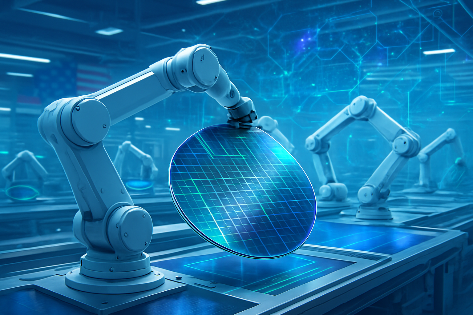
The integration of quantum computing with traditional semiconductor manufacturing represents a pivotal advancement in the quest for scalable and practical quantum systems, moving beyond isolated laboratory setups toward industrial fabrication. Recent breakthroughs center on leveraging complementary metal-oxide-semiconductor (CMOS) technology, the backbone of modern electronics, to fabricate and control qubits. Companies like Equal1 have successfully validated CMOS-compatible silicon spin qubit technology using commercial platforms such as GlobalFoundries' (NASDAQ:GFS) 22FDX, demonstrating the controlled formation of multiple quantum dots with tunable tunnel coupling, a crucial step for building dense qubit arrays. Intel (NASDAQ:INTC) has also made significant strides with its Horse Ridge and Tunnel Falls chips, which integrate quantum control logic directly with classical processors, operating efficiently within cryogenic environments. This includes the development of 48-dot array test chips on 300mm wafers, showcasing the potential for higher qubit densities. Furthermore, IMEC has reported coherent control of hole spin qubits in silicon with single-qubit gate fidelities exceeding 99.9%, incorporating on-chip cryogenic control electronics to enhance performance and scalability. Superconducting qubits are also benefiting from semiconductor integration, with researchers demonstrating their fabrication on high-resistivity silicon substrates, achieving coherence times comparable to those on sapphire substrates (e.g., T1 = 27µs, T2 = 6.6µs for high-resistivity silicon). The development of 3D integration techniques, such as superconducting through-silicon vias (TSVs), further enables high-density superconducting qubit arrays by facilitating complex interconnects between quantum and classical layers.
This integrated approach marks a significant departure from earlier quantum computing methodologies, which often relied on bulky, external control electronics and highly specialized, non-standard fabrication processes. Previous quantum systems frequently suffered from signal degradation and delays due to long wiring runs between qubits and room-temperature control systems, requiring car-sized hardware for cooling and support. By integrating classical control electronics (cryo-CMOS) directly on the same chip or in the same stack as the qubits, the new approach drastically reduces the physical footprint, minimizes signal loss, improves control speeds, and enhances qubit stability and gate accuracy, even at millikelvin temperatures. This strategic alignment with the established, multi-trillion-dollar semiconductor manufacturing infrastructure promises to unlock unprecedented scalability, enabling the potential for mass production and a significant reduction in the cost and accessibility of quantum technology. The use of existing silicon fabrication techniques helps address the crucial interconnect bottleneck and the complexity of wiring that previously limited the scaling of quantum processors to many thousands of qubits.
The initial reactions from the AI research community and industry experts to these advancements are a blend of considerable optimism and strategic caution. Many view this integration as ushering in a "transformative phase" and an "AI Supercycle," where AI not only consumes powerful chips but actively participates in their creation and optimization. Experts anticipate the emergence of "Quantum AI," accelerating complex AI algorithms, leading to more sophisticated machine learning models, enhanced data processing, and optimized large-scale logistics across various sectors, including drug discovery, materials science, climate modeling, cybersecurity, and financial risk control. There's a consensus that quantum computers will primarily complement classical systems, acting as powerful accelerators for specific, complex tasks in a hybrid quantum-classical computing paradigm, with some experts predicting quantum advantage for certain problems as early as 2025. The development of technologies like NVIDIA's (NASDAQ:NVDA) NVQLink, which directly couples quantum processors with GPU-accelerated supercomputers, is seen as a critical step in enabling hybrid quantum-classical applications and scaling quantum computing access. However, challenges remain significant, including the extreme fragility of quantum states necessitating ultra-low cryogenic temperatures and specialized packaging, continued high error rates requiring robust error correction protocols, the daunting task of scaling from tens to potentially millions of error-corrected qubits, and the current lack of standardization in hardware and software. There is also a recognized shortage of interdisciplinary talent with expertise spanning quantum physics, computer science, and engineering, which poses a bottleneck for the industry's growth.
Industry Shifts and Competitive Dynamics
The integration of quantum computing with traditional semiconductor manufacturing is poised to profoundly impact AI companies, tech giants, and startups, ushering in a new era of computational possibilities and intense competition. This synergy is driven by quantum computing's ability to tackle problems currently intractable for classical machines, particularly in complex optimization, simulation, and advanced AI.
The benefits will ripple across various types of companies. Traditional Semiconductor Manufacturers such as Intel (NASDAQ:INTC), Taiwan Semiconductor Manufacturing Company (NYSE:TSM) (TSMC), and Samsung (KRX:005930) are well-positioned to benefit by adapting their existing fabrication processes and integrating quantum simulation and optimization into their R&D pipelines. Foundries that embrace quantum-compatible workflows early may gain a strategic edge. AI Chip Developers like NVIDIA (NASDAQ:NVDA), a leader in AI-optimized GPUs, are actively exploring how their hardware can interface with and accelerate quantum workloads, introducing "NVQLink" to integrate conventional AI supercomputers with quantum processors. Tech Giants with Full-Stack Approaches, including IBM (NYSE:IBM), Google (NASDAQ:GOOGL), and Microsoft (NASDAQ:MSFT), are pursuing comprehensive strategies, controlling hardware, software, and cloud access to their quantum systems. IBM offers cloud-based access and is making strides in real-time quantum error correction. Google (Quantum AI) focuses on quantum supremacy and advancing algorithms for AI and machine learning, while Microsoft (Azure Quantum) is developing topological qubits and provides cloud access to various quantum hardware. Amazon (NASDAQ:AMZN) (AWS) offers Amazon Braket, a cloud-based quantum computing platform. Specialized Quantum Hardware and Software Startups, like IonQ (NYSE:IONQ) with trapped-ion technology or Diraq with silicon quantum dots, are crucial innovators, often specializing in niche areas or critical components like cryogenic electronics. Materials Science Companies will also benefit from quantum hardware accelerating the discovery of new materials.
The integration creates a new competitive landscape. Tech giants like IBM and Google are aiming to establish comprehensive ecosystems by controlling both hardware and software, and providing cloud access to their quantum systems. The most realistic near-term path involves hybrid classical-quantum systems, where quantum accelerators work in conjunction with classical computers, a strategy embraced by companies like NVIDIA with its CUDA-Q and NVQLink platforms. The "quantum advantage" race, where quantum computers demonstrably outperform classical systems, is a key driver of competition, with experts anticipating this milestone within the next 3 to 10 years. The immense cost of quantum R&D and specialized infrastructure could exacerbate the technological divide, and a shortage of quantum computing expertise also hampers widespread adoption. There's a synergistic relationship where AI is increasingly applied to accelerate quantum and semiconductor design, and conversely, quantum computing enhances AI, creating a virtuous cycle benefiting leaders in both fields. Cloud deployment is a dominant market strategy, democratizing access to quantum resources and lowering entry barriers.
Potential disruptions to existing products or services are significant. The specialized requirements of quantum processors will necessitate rethinking traditional chip designs, manufacturing processes, and materials, potentially leading to a shift in demand towards quantum-enhanced AI hardware. Quantum computing promises to accelerate complex AI algorithms, leading to more sophisticated machine learning models, enhanced data processing, and optimized large-scale logistics, potentially enabling entirely new forms of AI. Quantum machine learning could dramatically speed up how fast AI learns and adapts, cutting training times and reducing energy consumption. Quantum algorithms can revolutionize fields like supply chain routing, financial modeling, drug discovery, and materials science. Furthermore, quantum computing poses a threat to current public-key encryption standards ("Q-Day" around 2030), necessitating a shift to quantum-resistant cryptography, which will disrupt existing cybersecurity products and services but also create a new market for quantum-safe solutions. Quantum technology offers a more sustainable, efficient, and high-performance solution for AI, dramatically lowering costs and increasing scalability while overcoming the energy limitations of today's classical systems.
In terms of market positioning and strategic advantages, smart semiconductor players are investing modularly, developing quantum-compatible process steps and control electronics. Companies are increasingly embracing hybrid approaches, where quantum computers act as accelerators, integrating with classical supercomputers. Strategic partnerships and collaborations are critical for accelerating R&D and bringing quantum solutions to market. Startups often gain an advantage by specializing in specific qubit architectures, quantum materials, or quantum-classical integration. Tech giants offering cloud-accessible quantum systems gain a significant advantage by democratizing access. Companies are strategically targeting sectors like finance, logistics, pharmaceuticals, and materials science, where quantum computing can offer significant competitive advantages. Early adaptation of foundries to quantum-compatible workflows, materials, and design philosophies stands to gain a strategic edge, with advancements in EUV lithography, atomic-layer processes, and 3D integration driven by quantum chip demands also improving mainstream chip production. Companies like NVIDIA leverage their existing GPU expertise and software platforms (CUDA) to bridge classical and quantum computing, providing a faster path to market for high-end computing applications.
A New Frontier: Broader Implications and Challenges
The integration of quantum computing with traditional semiconductor manufacturing represents a pivotal technological convergence with profound wider significance, especially within the evolving Artificial Intelligence (AI) landscape. This synergy promises to unlock unprecedented computational power, redefine manufacturing processes, and overcome current limitations in AI development.
This integration is poised to revolutionize advanced material discovery and design, enabling the rapid identification and design of advanced materials for more efficient and powerful chips. It will also significantly impact process optimization and manufacturing efficiency by simulating fabrication processes at the quantum level, reducing errors and improving yield. Enhanced chip design capabilities will facilitate the creation of more complex and efficient semiconductor architectures, accelerating the development of advanced chips. Furthermore, quantum computing can offer robust solutions for optimizing intricate global supply chains in the semiconductor industry, improving demand forecasting, inventory management, and logistics planning. As traditional manufacturing techniques approach physical limits, quantum computing offers a promising avenue for enhancing semiconductor design and production processes, potentially evolving or revitalizing Moore's Law into new paradigms.
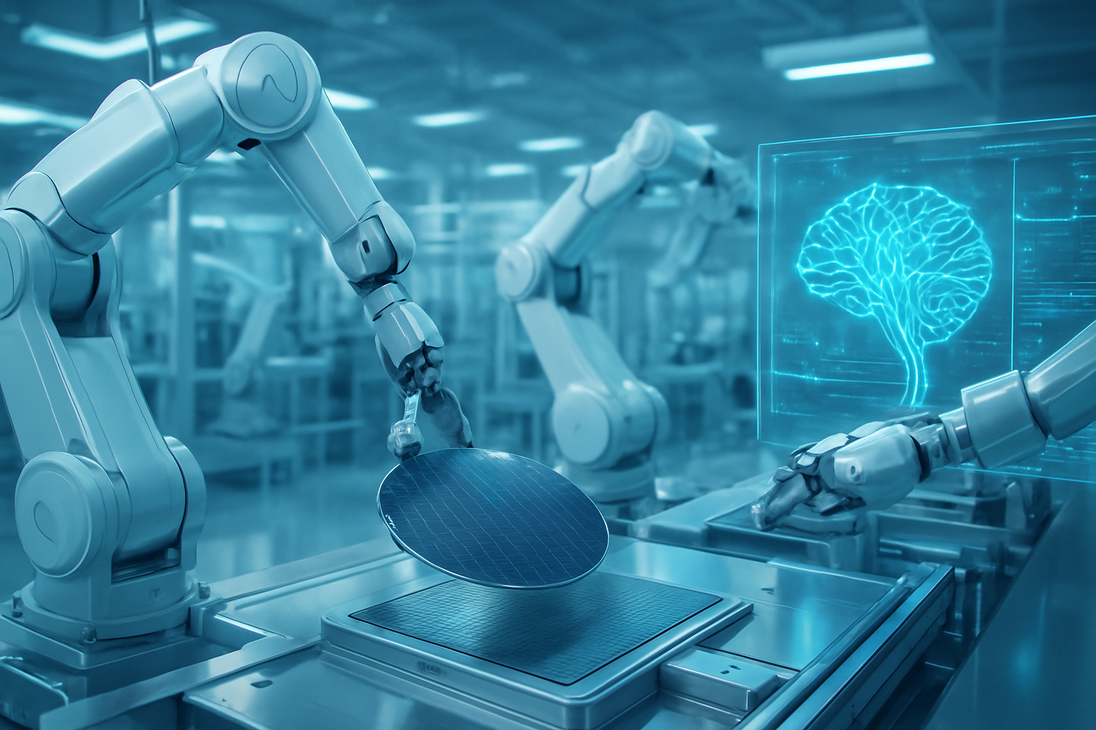
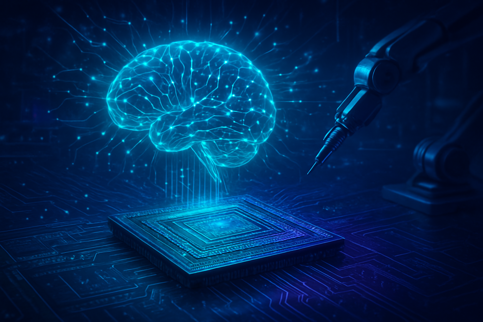
This integration is not merely a technological upgrade but a paradigm shift that will profoundly reshape the broader AI landscape. It has the potential to supercharge AI by offering new ways to train models, optimize algorithms, and tackle complex problems beyond the reach of today's classical computers. The insatiable demand for greater computational power and energy efficiency for deep learning and large language models is pushing classical hardware to its breaking point; quantum-semiconductor integration offers a vital pathway to overcome these bottlenecks, providing exponential speed-ups for certain tasks. Quantum machine learning algorithms could process and classify large datasets more efficiently, leading to faster training of AI models and enhanced optimization. Many experts view this integration as a crucial step towards Artificial General Intelligence (AGI), enabling AI models to solve problems currently intractable for classical systems. Conversely, AI itself is being applied to accelerate quantum and semiconductor design, creating a virtuous cycle of innovation.
The impacts are far-reaching, promising economic growth and an industrial renaissance across various sectors. Quantum-enhanced AI can accelerate scientific breakthroughs, such as drug discovery and new materials development. Quantum computers have the potential for more energy-efficient AI algorithms, crucial for addressing the high power demands of modern AI models. While quantum computers pose a threat to current encryption methods, they are also key to developing quantum-resistant cryptographic algorithms, vital for cybersecurity in a post-quantum world. Leveraging existing semiconductor manufacturing infrastructure is crucial for scaling up quantum processors and making quantum computing more reliable and practical.
Despite its transformative potential, the integration of quantum computing and semiconductors presents several challenges and concerns. Quantum systems require specialized environments, such as cryogenic cooling, which significantly increases costs and complexity. There is a persistent talent shortage in quantum computing and its integration. Aligning quantum advancements with existing semiconductor processes and ensuring seamless communication between quantum modules and classical IT infrastructure is technically complex. Qubits are fragile and susceptible to noise and decoherence, making error correction a critical hurdle. The immense cost of quantum R&D could exacerbate the technological divide. Ethical considerations surrounding highly advanced AI powered by quantum computing also raise concerns regarding potential biases and the need for robust regulatory frameworks.
This development is often described as more than just an incremental upgrade; it's considered a fundamental paradigm shift, akin to the transition from Central Processing Units (CPUs) to Graphics Processing Units (GPUs) that fueled the deep learning revolution. Just as GPUs enabled the parallel processing needed for deep learning, quantum computing introduces unprecedented parallelism and data representation capabilities through qubits, moving beyond the traditional limitations of classical physics. Demonstrations like Google's (NASDAQ:GOOGL) Sycamore processor achieving "quantum supremacy" in 2019, solving a complex problem faster than the world's most powerful supercomputers, highlight this transformative potential.
Charting the Future: Predictions and Pathways
The integration of quantum computing with traditional semiconductor manufacturing is poised to revolutionize the technology landscape, promising unprecedented computational power and innovative solutions across various industries. This synergy is expected to unfold through near-term advancements and long-term paradigm shifts, addressing complex challenges and opening doors to new applications.
In the near-term (next 5-10 years), the focus will be on hybrid quantum-classical computing architectures, where quantum processors act as specialized accelerators. This involves classical semiconductor-based interconnects ensuring seamless data exchange. Companies like Intel (NASDAQ:INTC) are actively pursuing silicon spin qubits due to their scalability with advanced lithography and are developing cryogenic control chips like Horse Ridge II, simplifying quantum system operations. By 2025, development teams are expected to increasingly prioritize qubit precision and performance over merely increasing qubit count. Long-term developments envision achieving large-scale quantum processors with thousands or millions of stable qubits, necessitating advanced error correction mechanisms and new semiconductor fabrication facilities capable of handling ultra-pure materials and extreme precision lithography. Innovations in materials science, lithography, and nanofabrication, driven by quantum demands, will spill over into mainstream chip production.
The integration promises a wide array of applications. In semiconductor manufacturing, quantum algorithms can enhance AI models for improved chip design, enable real-time process monitoring, accelerate material discovery, and optimize fabrication processes. For supply chain management, quantum algorithms can improve demand forecasting, inventory management, and logistics planning. Broader industry impacts include enhanced cybersecurity through quantum cryptography and quantum-resistant algorithms, dramatically reduced AI training times and more sophisticated machine learning models, accelerated drug discovery by simulating molecular interactions, enhanced financial modeling, and more efficient climate modeling.
Despite the immense potential, several significant challenges must be overcome. These include the high infrastructure requirements for cryogenic cooling, a persistent talent shortage, complex compatibility issues between quantum and classical components, and the critical need for maintaining quantum coherence and robust error correction. High research and development costs, low manufacturing yields, and the existence of competing qubit architectures also pose hurdles. Managing thermal dissipation, mitigating gate-oxide defects, and developing efficient interfaces and control electronics are crucial. Furthermore, quantum computing introduces new types of data that require different storage and management approaches.
Experts foresee a transformative future. Many anticipate reaching "quantum advantage"—where quantum computers demonstrably outperform classical machines for certain useful tasks—within the next 3 to 5 years, with some extending this to 5 to 10 years. There's a growing awareness of "Q-Day," estimated around 2030, when quantum computers could break current public-key encryption standards, accelerating investment in quantum-resistant cryptography. By 2025, a greater emphasis will be placed on qubit precision and performance rather than just the raw qubit count. The quantum ecosystem will mature with increased collaboration, driving faster commercialization and adoption, with "quantum platforms" offering seamless integration of classical, AI, and quantum resources. Quantum design tools are expected to become standard in advanced semiconductor R&D within the next decade. Quantum computing is not expected to replace traditional semiconductors entirely but will act as a powerful catalyst for progress, positioning early adaptors at the forefront of the next computing revolution. The global quantum hardware market, specifically the quantum chip market, is projected to reach USD 7.04 billion by 2032.
A New Era of Computational Power Dawns
The integration of quantum computing with traditional semiconductor manufacturing marks a pivotal moment in the evolution of technology, promising to redefine the very limits of computation and innovation. This symbiotic relationship is set to usher in an era of hybrid quantum-classical systems, where the exponential power of quantum mechanics augments the established reliability of silicon-based electronics. Key takeaways from this impending revolution include the critical advancements in CMOS-compatible qubit fabrication, the development of specialized cryogenic control electronics, and the strategic shift towards hybrid architectures that leverage the strengths of both classical and quantum paradigms.
This development's significance in AI history cannot be overstated. It represents a potential leap comparable to, if not exceeding, the transition from CPUs to GPUs that fueled the deep learning revolution. By enabling the processing of previously intractable problems, this integration offers the computational horsepower necessary to unlock more sophisticated AI models, accelerate scientific discovery, and optimize complex systems across nearly every industry. While challenges such as qubit fragility, error correction, and the immense cost of R&D remain, the concerted efforts of tech giants, specialized startups, and academic institutions are steadily pushing the boundaries of what's possible.
Looking ahead, the coming weeks and months will likely see continued breakthroughs in qubit stability and coherence, further integration of control electronics onto the quantum chip, and the maturation of software platforms designed to bridge the classical-quantum divide. The race for "quantum advantage" will intensify, potentially leading to demonstrable real-world applications within the next few years. As the semiconductor industry adapts to meet the exacting demands of quantum technologies, we can expect a cascade of innovations that will not only advance quantum computing but also push the boundaries of classical chip design and manufacturing. The long-term impact promises a future where AI, supercharged by quantum capabilities, tackles humanity's most complex problems, from climate change to personalized medicine, fundamentally transforming our world.
This content is intended for informational purposes only and represents analysis of current AI developments.
TokenRing AI delivers enterprise-grade solutions for multi-agent AI workflow orchestration, AI-powered development tools, and seamless remote collaboration platforms.
For more information, visit https://www.tokenring.ai/.