Tag: Semiconductor Testing

  • The Unsung Hero: How Semiconductor Testing Fuels the AI Revolution, Driving Growth for Leaders Like Teradyne

    The Unsung Hero: How Semiconductor Testing Fuels the AI Revolution, Driving Growth for Leaders Like Teradyne

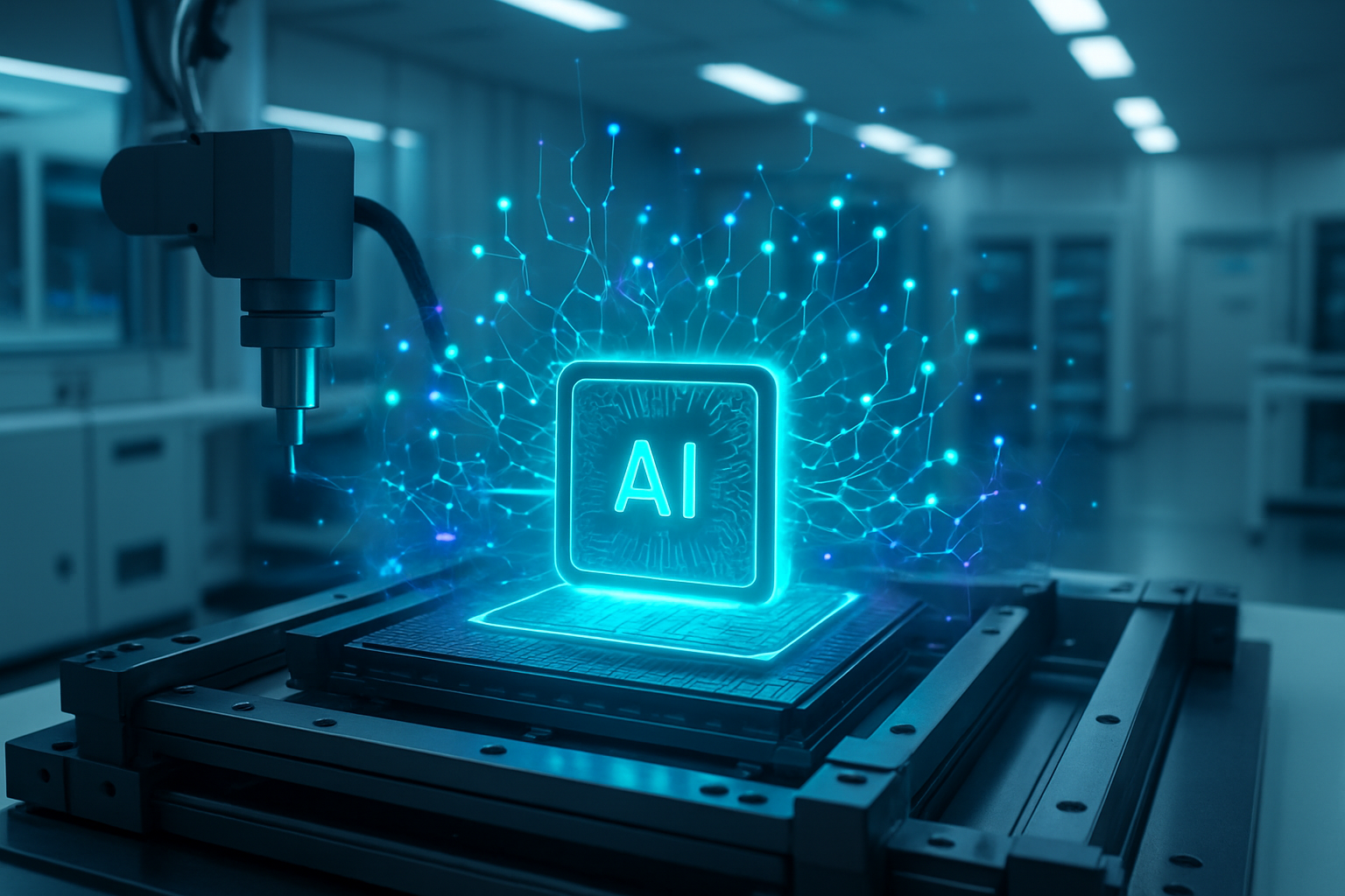
    The relentless march of Artificial Intelligence (AI) is fundamentally reshaping the technology landscape, and at its core lies the intricate world of semiconductor chips. While much attention is paid to the breakthroughs in AI algorithms and applications, an equally crucial, though often overlooked, element is the rigorous and sophisticated testing required for these advanced processors. This critical need for robust semiconductor testing is not only ensuring the quality and reliability of AI hardware but is also driving significant growth for specialized companies like Teradyne (NASDAQ: TER), positioning them as indispensable partners in the AI revolution.

    The burgeoning field of AI demands chips of unprecedented complexity, powerful processing capabilities, and high data throughput. These attributes necessitate meticulous testing to guarantee their performance, reliability, and efficiency across demanding applications, from massive data centers to intelligent edge devices and autonomous systems. The immediate significance of this trend is multifaceted: it accelerates development cycles, manages exponential complexity, enhances chip quality and security, and fuels substantial market growth and investment across the entire semiconductor ecosystem. In essence, semiconductor testing has evolved from a secondary step to a strategic imperative, critical for innovation, quality, and rapid market readiness in the age of AI.

    The Technical Crucible: Advanced Testing for AI's Complex Brains

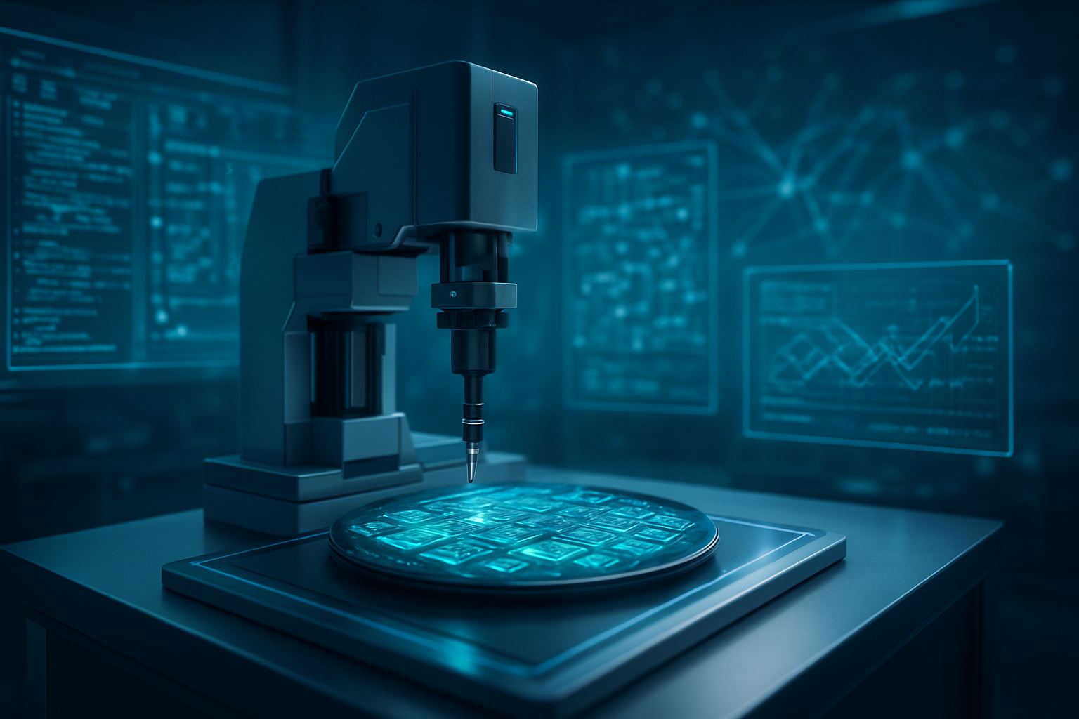
    AI chips represent a paradigm shift in semiconductor architecture, moving beyond traditional CPU and GPU designs to incorporate highly specialized accelerators like NPUs (Neural Processing Units), TPUs (Tensor Processing Units), and custom ASICs (Application-Specific Integrated Circuits). These chips are characterized by their massive core counts, extreme parallelism, and intricate interconnects designed for high-bandwidth data movement—all optimized for deep learning and machine learning workloads. Testing such intricate designs presents unique challenges that differentiate it significantly from previous approaches.

    Unlike the relatively predictable instruction sets and data flows of general-purpose processors, AI chips operate on vast matrices of data, often with mixed-precision arithmetic and highly pipelined execution. This requires advanced automated test equipment (ATE) to verify functionality across billions of transistors operating at blazing speeds. Key technical considerations include ensuring signal integrity at multi-gigahertz frequencies, managing power delivery and thermal dissipation under heavy loads, and validating the accuracy of complex arithmetic units crucial for AI model inference and training. Furthermore, the sheer volume of data processed by these chips demands sophisticated data-intensive test patterns and analytics to detect subtle performance degradations or latent defects. Early defect detection at the wafer level is paramount, as it significantly improves yields, accelerates development timelines, and prevents costly issues from propagating into final production stages. Initial reactions from the AI research community and industry experts highlight the growing recognition that robust testing is not merely a quality control measure but an integral part of the design process itself, with "design for testability" becoming a core principle for next-generation AI accelerators.

    Shifting Sands: Competitive Implications for the AI Industry

    The escalating demand for advanced AI chip testing has profound implications for AI companies, tech giants, and startups alike, creating a new competitive landscape where access to cutting-edge testing solutions is a strategic advantage. Companies like Teradyne (NASDAQ: TER), with its robust portfolio of automated test equipment, stand to benefit immensely from this development. Their ability to provide high-performance, high-throughput test solutions for complex System-on-a-Chip (SOC) designs tailored for AI applications positions them at the forefront of this wave. Teradyne's recent financial reports underscore this trend, with strong revenue growth driven by AI-related demand across compute, networking, and memory segments, leading to upward revisions in analyst price targets.

    Major AI labs and tech companies, including NVIDIA (NASDAQ: NVDA), Google (NASDAQ: GOOGL), and Intel (NASDAQ: INTC), which are heavily invested in designing their own AI accelerators, are directly impacted. They require sophisticated testing partners or in-house capabilities to bring their chips to market reliably and efficiently. This creates a competitive bottleneck where companies with superior testing methodologies can achieve faster time-to-market and higher quality products. Startups entering the AI hardware space face even greater pressure, as the cost and complexity of advanced testing can be a significant barrier to entry. This dynamic could lead to increased consolidation in the AI hardware sector or foster tighter partnerships between chip designers and ATE providers. The need for specialized testing also creates potential disruption to existing products, as older, less rigorously tested chips may struggle to meet the performance and reliability demands of critical AI applications, thereby accelerating the adoption of new, thoroughly validated hardware.

    The Broader Canvas: AI Testing's Wider Significance

    The pivotal role of semiconductor testing in AI development fits seamlessly into the broader AI landscape and ongoing technological trends. It underscores a fundamental shift where hardware, once seen as a static foundation, is now a dynamic and rapidly evolving component critical to AI's progress. The increasing complexity of AI models, particularly generative AI, demands ever more powerful and efficient hardware, which in turn necessitates more sophisticated testing. This creates a virtuous cycle where AI itself is being leveraged to enhance testing processes, with AI and Machine Learning (ML) algorithms identifying subtle patterns and anomalies in test data, predicting potential failures, and optimizing test sequences for greater efficiency and speed.

    The impacts extend beyond mere chip quality. Enhanced testing contributes to the overall reliability and security of AI systems, crucial for deployment in sensitive applications like autonomous vehicles, medical diagnostics, and critical infrastructure. Potential concerns, however, include the escalating cost of advanced ATE, which could become a barrier for smaller players, and the challenge of keeping pace with the rapid innovation cycle of AI chip design. Comparisons to previous AI milestones, such as the rise of GPUs for deep learning, highlight that breakthroughs in software are often enabled by underlying hardware advancements and the infrastructure, including testing, that supports them. This era marks a maturation of the AI industry, where robust engineering practices, including thorough testing, are becoming as important as algorithmic innovation. The global AI chip market is experiencing explosive growth, projected to reach hundreds of billions of dollars, and the market for AI in semiconductor ATE analysis is similarly expanding, cementing the long-term significance of this trend.

    The Road Ahead: Future Developments in AI Chip Testing

    Looking ahead, the landscape of AI chip testing is poised for continuous evolution, driven by the relentless pace of AI innovation. Near-term developments are expected to focus on further integrating AI and ML directly into the test equipment itself, allowing for more intelligent test generation, real-time fault diagnosis, and predictive maintenance of the test systems. We can anticipate the proliferation of "in-situ" testing methodologies, where chips are tested not just for individual components but for their performance within an emulated system environment, mimicking real-world AI workloads. The rise of advanced packaging technologies, such as chiplets and 3D stacking, will also drive new testing challenges and solutions, as inter-chiplet communication and thermal management become critical test vectors.

    Long-term developments will likely see the emergence of fully autonomous testing systems that can adapt and learn, optimizing test coverage and efficiency without human intervention. Potential applications and use cases on the horizon include "self-healing" chips that can identify and reconfigure around defective elements, and AI-powered design tools that incorporate testability from the earliest stages of chip conception. Challenges that need to be addressed include the standardization of AI chip testing protocols, the development of universal benchmarks for AI accelerator performance and reliability, and the need for a highly skilled workforce capable of operating and developing these complex test systems. Experts predict a continued convergence of design, manufacturing, and testing, with AI acting as the connective tissue, enabling a more holistic and efficient chip development lifecycle.

    The Cornerstone of AI's Future: A Comprehensive Wrap-up

    The crucial role of semiconductor testing in AI development is an undeniable and increasingly significant facet of the modern technology landscape. As AI continues its rapid ascent, the need for meticulously tested, high-performance chips has elevated companies like Teradyne (NASDAQ: TER) to the status of critical enablers, experiencing substantial growth as a direct result. The key takeaway is clear: robust testing is not an afterthought but a foundational pillar supporting the entire AI edifice, ensuring the reliability, efficiency, and ultimate success of AI applications across every sector.

    This development marks a significant milestone in AI history, underscoring the industry's maturation from pure research to large-scale, dependable deployment. The long-term impact will be profound, leading to more resilient AI systems, faster innovation cycles, and a more competitive and specialized semiconductor industry. What to watch for in the coming weeks and months includes further advancements in AI-driven test automation, the integration of advanced packaging test solutions, and strategic partnerships between chip designers and ATE providers. The unsung hero of semiconductor testing is finally getting its well-deserved recognition, proving that the future of AI is as much about rigorous validation as it is about groundbreaking algorithms.


    This content is intended for informational purposes only and represents analysis of current AI developments.

    TokenRing AI delivers enterprise-grade solutions for multi-agent AI workflow orchestration, AI-powered development tools, and seamless remote collaboration platforms.
    For more information, visit https://www.tokenring.ai/.

  • Teradyne’s UltraPHY 224G: Fortifying the Foundation of Next-Gen AI

    Teradyne’s UltraPHY 224G: Fortifying the Foundation of Next-Gen AI

    In an era defined by the escalating complexity and performance demands of artificial intelligence, the reliability of the underlying hardware is paramount. A significant leap forward in ensuring this reliability comes from Teradyne Inc. (NASDAQ: TER), with the introduction of its UltraPHY 224G instrument for the UltraFLEXplus platform. This cutting-edge semiconductor test solution is engineered to tackle the formidable challenges of verifying ultra-high-speed physical layer (PHY) interfaces, a critical component for the functionality and efficiency of advanced AI chips. Its immediate significance lies in its ability to enable robust testing of the intricate interconnects that power modern AI accelerators, ensuring that the massive datasets fundamental to AI applications can be transferred with unparalleled speed and accuracy.

    The advent of the UltraPHY 224G marks a pivotal moment for the AI industry, addressing the urgent need for comprehensive validation of increasingly sophisticated chip architectures, including chiplets and advanced packaging. As AI workloads grow more demanding, the integrity of high-speed data pathways within and between chips becomes a bottleneck if not meticulously tested. Teradyne's new instrument provides the necessary bandwidth and precision to verify these interfaces at speeds up to 224 Gb/s PAM4, directly contributing to the development of "Known Good Die" (KGD) workflows crucial for multi-chip AI modules. This advancement not only accelerates the deployment of high-performance AI hardware but also significantly bolsters the overall quality and reliability, laying a stronger foundation for the future of artificial intelligence.

    Advancing the Frontier of AI Chip Testing

    The UltraPHY 224G represents a significant technical leap in the realm of semiconductor test instruments, specifically engineered to meet the burgeoning demands of AI chip validation. At its core, this instrument boasts support for unprecedented data rates, reaching up to 112 Gb/s Non-Return-to-Zero (NRZ) and an astonishing 224 Gb/s (112 Gbaud) using PAM4 (Pulse Amplitude Modulation 4-level) signaling. This capability is critical for verifying the integrity of the ultra-high-speed communication interfaces prevalent in today's most advanced AI accelerators, data centers, and silicon photonics applications. Each UltraPHY 224G instrument integrates eight full-duplex differential lanes and eight receive-only differential lanes, delivering over 50 GHz of signal delivery bandwidth to ensure unparalleled signal fidelity during testing.

    What sets the UltraPHY 224G apart is its sophisticated architecture, combining Digital Storage Oscilloscope (DSO), Bit Error Rate Tester (BERT), and Arbitrary Waveform Generator (AWG) capabilities into a single, comprehensive solution. This integrated approach allows for both high-volume production testing and in-depth characterization of physical layer interfaces, providing engineers with the tools to not only detect pass/fail conditions but also to meticulously analyze signal quality, jitter, eye height, eye width, and TDECQ for PAM4 signals. This level of detailed analysis is crucial for identifying subtle performance issues that could otherwise compromise the long-term reliability and performance of AI chips operating under intense, continuous loads.

    The UltraPHY 224G builds upon Teradyne’s existing UltraPHY portfolio, extending the capabilities of its UltraPHY 112G instrument. A key differentiator is its ability to coexist with the UltraPHY 112G on the same UltraFLEXplus platform, offering customers seamless scalability and flexibility to test a wide array of current and future high-speed interfaces without necessitating a complete overhaul of their test infrastructure. This forward-looking design, developed with MultiLane modules, sets a new benchmark for test density and signal fidelity, delivering "bench-quality" signal generation and measurement in a production test environment. This contrasts sharply with previous approaches that often required separate, less integrated solutions, increasing complexity and cost.

    Initial reactions from the AI research community and industry experts have been overwhelmingly positive. Teradyne's (NASDAQ: TER) strategic focus on the compute semiconductor test market, particularly AI ASICs, has resonated well, with the company reporting significant wins in non-GPU AI ASIC designs. Financial analysts have recognized the company's strong positioning, raising price targets and highlighting its growing potential in the AI compute sector. Roy Chorev, Vice President and General Manager of Teradyne's Compute Test Division, emphasized the instrument's capability to meet "the most demanding next-generation PHY test requirements," assuring that UltraPHY investments would support evolving chiplet-based architectures and Known Good Die (KGD) workflows, which are becoming indispensable for advanced AI system integration.

    Strategic Implications for the AI Industry

    The introduction of Teradyne's UltraPHY 224G for UltraFLEXplus carries profound strategic implications across the entire AI industry, from established tech giants to nimble startups specializing in AI hardware. The instrument's unparalleled ability to test high-speed interfaces at 224 Gb/s PAM4 is a game-changer for companies designing and manufacturing AI accelerators, Graphics Processing Units (GPUs), Neural Processing Units (NPUs), and other custom AI silicon. These firms, which are at the forefront of AI innovation, can now rigorously validate their increasingly complex chiplet-based designs and advanced packaging solutions, ensuring the robustness and performance required for the next generation of AI workloads. This translates into accelerated product development cycles and the ability to bring more reliable, high-performance AI solutions to market faster.

    Major tech giants such as NVIDIA Corp. (NASDAQ: NVDA), Intel Corp. (NASDAQ: INTC), Advanced Micro Devices Inc. (NASDAQ: AMD), Google (NASDAQ: GOOGL), Amazon (NASDAQ: AMZN), Microsoft (NASDAQ: MSFT), and Meta (NASDAQ: META), deeply invested in developing their own custom AI hardware and expansive data center infrastructures, stand to benefit immensely. The UltraPHY 224G provides the high-volume, high-fidelity testing capabilities necessary to validate their advanced AI accelerators, high-speed network interfaces, and silicon photonics components at production scale. This ensures that these companies can maintain their competitive edge in AI innovation, improve hardware quality, and potentially reduce the significant costs and time traditionally associated with testing highly intricate hardware. The ability to confidently push the boundaries of AI chip design, knowing that rigorous validation is achievable, empowers these industry leaders to pursue even more ambitious projects.

    For AI hardware startups, the UltraPHY 224G presents a dual-edged sword of opportunity and challenge. On one hand, it democratizes access to state-of-the-art testing capabilities that were once the exclusive domain of larger entities, enabling startups to validate their innovative designs against the highest industry standards. This can be crucial for overcoming reliability concerns and accelerating market entry for novel high-speed AI chips. On the other hand, the substantial capital expenditure associated with such advanced Automated Test Equipment (ATE) might be prohibitive for nascent companies. This could lead to a reliance on third-party test houses equipped with UltraPHY 224G, thereby evening the playing field in terms of validation quality and potentially fostering a new ecosystem of specialized test service providers.

    The competitive landscape within AI hardware is set to intensify. Early adopters of the UltraPHY 224G will gain a significant competitive advantage through accelerated time-to-market for superior AI hardware. This will put immense pressure on competitors still relying on older or less capable testing equipment, as their ability to efficiently validate complex, high-speed designs will be compromised, potentially leading to delays or quality issues. The solution also reinforces Teradyne's (NASDAQ: TER) market positioning as a leader in next-generation testing, offering a "future-proof" investment for customers through its scalable UltraFLEXplus platform. This strategic advantage, coupled with the integrated testing ecosystem provided by IG-XL software, solidifies Teradyne's role as an enabler of innovation in the rapidly evolving AI hardware domain.

    Broader Significance in the AI Landscape

    Teradyne's UltraPHY 224G is not merely an incremental upgrade in semiconductor testing; it represents a foundational technology underpinning the broader AI landscape and its relentless pursuit of higher performance. In an era where AI models, particularly large language models and complex neural networks, demand unprecedented computational power and data throughput, the reliability of the underlying hardware is paramount. This instrument directly addresses the critical need for high-speed, high-fidelity testing of the interconnects and memory systems that are essential for AI accelerators and GPUs to function efficiently. Its support for data rates up to 224 Gb/s PAM4 directly aligns with the industry trend towards advanced interfaces like PCIe Gen 7, Compute Express Link (CXL), and next-generation Ethernet, all vital for moving massive datasets within and between AI processing units.

    The impact of the UltraPHY 224G is multifaceted, primarily revolving around enabling the reliable development and production of next-generation AI hardware. By providing "bench-quality" signal generation and measurement for production testing, it ensures high test density and signal fidelity for semiconductor interfaces. This is crucial for improving overall chip yields and mitigating the enormous costs associated with defects in high-value AI accelerators. Furthermore, its support for chiplet-based architectures and advanced packaging is vital. These modern designs, which combine multiple chiplets into a single unit for performance gains, introduce new reliability risks and testing challenges. The UltraPHY 224G ensures that these complex integrations can be thoroughly verified, accelerating the development and deployment of new AI applications and hardware.

    Despite its advancements, the AI hardware testing landscape, and by extension, the application of UltraPHY 224G, faces inherent challenges. The extreme complexity of AI chips, characterized by ultra-high power consumption, ultra-low voltage requirements, and intricate heterogeneous integration, complicates thermal management, signal integrity, and power delivery during testing. The increasing pin counts and the use of 2.5D and 3D IC packaging techniques also introduce physical and electrical hurdles for probe cards and maintaining signal integrity. Additionally, AI devices generate massive amounts of test data, requiring sophisticated analysis and management, and the market for test equipment remains susceptible to semiconductor industry cycles and geopolitical factors.

    Compared to previous AI milestones, which largely focused on increasing computational power (e.g., the rise of GPUs, specialized AI accelerators) and memory bandwidth (e.g., HBM advancements), the UltraPHY 224G represents a critical enabler rather than a direct computational breakthrough. It addresses a bottleneck that has often hindered the reliable validation of these complex components. By moving beyond traditional testing approaches, which are often insufficient for the highly integrated and data-intensive nature of modern AI semiconductors, the UltraPHY 224G provides the precision required to test next-generation interconnects and High Bandwidth Memory (HBM) at speeds previously difficult to achieve in production environments. This ensures the consistent, error-free operation of AI hardware, which is fundamental for the continued progress and trustworthiness of artificial intelligence.

    The Road Ahead for AI Chip Verification

    The journey for Teradyne's UltraPHY 224G and its role in AI chip verification is just beginning, with both near-term and long-term developments poised to shape the future of artificial intelligence hardware. In the near term, the UltraPHY 224G, having been released in October 2025, is immediately addressing the burgeoning demands for next-generation high-speed interfaces. Its seamless integration and co-existence with the UltraPHY 112G on the UltraFLEXplus platform offer customers unparalleled flexibility, allowing them to test a diverse range of current and future high-speed interfaces without requiring entirely new test infrastructures. Teradyne's broader strategy, encompassing platforms like Titan HP for AI and cloud infrastructure, underscores a comprehensive effort to remain at the forefront of semiconductor testing innovation.

    Looking further ahead, the UltraPHY 224G is strategically positioned for sustained relevance in a rapidly advancing technological landscape. Its inherent design supports the continued evolution of chiplet-based architectures, advanced packaging techniques, and Known Good Die (KGD) workflows, which are becoming standard for upcoming generations of AI chips. Experts predict that the AI inference chip market alone will experience explosive growth, surpassing $25 billion by 2027 with a compound annual growth rate (CAGR) exceeding 30% from 2025. This surge, driven by increasing demand across cloud services, automotive applications, and a wide array of edge devices, will necessitate increasingly sophisticated testing solutions like the UltraPHY 224G. Moreover, the long-term trend points towards AI itself making the testing process smarter, with machine learning improving wafer testing by enabling faster detection of yield issues and more accurate failure prediction.

    The potential applications and use cases for the UltraPHY 224G are vast and critical for the advancement of AI. It is set to play a pivotal role in testing cloud and edge AI processors, high-speed data center and silicon photonics (SiPh) interconnects, and next-generation communication technologies like mmWave and 5G/6G devices. Furthermore, its capabilities are essential for validating advanced packaging and chiplet architectures, as well as high-speed SERDES (Serializer/Deserializer) and backplane transceivers. These components form the backbone of modern AI infrastructure, and the UltraPHY 224G ensures their integrity and performance.

    However, the road ahead is not without its challenges. The increasing complexity and scale of AI chips, with their large die sizes, billions of transistors, and numerous cores, push the limits of traditional testing. Maintaining signal integrity across thousands of ultra-fine-pitch I/O contacts, managing the substantial heat generated by AI chips, and navigating the physical complexities of advanced packaging are significant hurdles. The sheer volume of test data generated by AI devices, projected to increase eightfold for SOC chips by 2025 compared to 2018, demands fundamental improvements in ATE architecture and analysis. Experts like Stifel have raised Teradyne's stock price target, citing its growing position in the compute semiconductor test market. There's also speculation that Teradyne is strategically aiming to qualify as a test supplier for major GPU developers like NVIDIA Corp. (NASDAQ: NVDA), indicating an aggressive pursuit of market share in the high-growth AI compute sector. The integration of AI into the design, manufacturing, and testing of chips signals a new era of intelligent semiconductor engineering, with advanced wafer-level testing being central to this transformation.

    A New Era of AI Hardware Reliability

    Teradyne Inc.'s (NASDAQ: TER) UltraPHY 224G for UltraFLEXplus marks a pivotal moment in the quest for reliable and high-performance AI hardware. This advanced high-speed physical layer (PHY) performance testing instrument is a crucial extension of Teradyne's existing UltraPHY portfolio, meticulously designed to meet the most demanding test requirements of next-generation semiconductor interfaces. Key takeaways include its support for unprecedented data rates up to 224 Gb/s PAM4, its integrated DSO+BERT architecture for comprehensive signal analysis, and its seamless compatibility with the UltraPHY 112G on the same UltraFLEXplus platform. This ensures unparalleled flexibility for customers navigating the complex landscape of chiplet-based architectures, advanced packaging, and Known Good Die (KGD) workflows—all essential for modern AI chips.

    This development holds significant weight in the history of AI, serving as a critical enabler for the ongoing hardware revolution. As AI accelerators and cloud infrastructure devices grow in complexity and data intensity, the need for robust, high-speed testing becomes paramount. The UltraPHY 224G directly addresses this by providing the necessary tools to validate the intricate, high-speed physical interfaces that underpin AI computations and data transfer. By ensuring the quality and optimizing the yield of these highly complex, multi-chip designs, Teradyne is not just improving testing; it's accelerating the deployment of next-generation AI hardware, which in turn fuels advancements across virtually every AI application imaginable.

    The long-term impact of the UltraPHY 224G is poised to be substantial. Positioned as a future-proof solution, its scalability and adaptability to evolving PHY interfaces suggest a lasting influence on semiconductor testing infrastructure. By enabling the validation of increasingly higher data rates and complex architectures, Teradyne is directly contributing to the sustained progress of AI and high-performance computing. The ability to guarantee the quality and performance of these foundational hardware components will be instrumental for the continued growth and innovation in the AI sector for years to come, solidifying Teradyne's leadership in the rapidly expanding compute semiconductor test market.

    In the coming weeks and months, industry observers should closely monitor the adoption rate of the UltraPHY 224G by major players in the AI and data center sectors. Customer testimonials and design wins from leading chip manufacturers will provide crucial insights into its real-world impact on development and production cycles for AI chips. Furthermore, Teradyne's financial reports will offer a glimpse into the market penetration and revenue contributions of this new instrument. The evolution of industry standards for high-speed interfaces and how Teradyne's flexible UltraPHY platform adapts to support emerging modulation formats will also be key indicators. Finally, keep an eye on the competitive landscape, as other automated test equipment (ATE) providers will undoubtedly respond to these demanding AI chip testing requirements, shaping the future of AI hardware validation.


    This content is intended for informational purposes only and represents analysis of current AI developments.

    TokenRing AI delivers enterprise-grade solutions for multi-agent AI workflow orchestration, AI-powered development tools, and seamless remote collaboration platforms.
    For more information, visit https://www.tokenring.ai/.