Tag: Semiconductor

  • RISC-V Rises: An Open-Source Revolution Poised to Disrupt ARM’s Chip Dominance

    RISC-V Rises: An Open-Source Revolution Poised to Disrupt ARM’s Chip Dominance

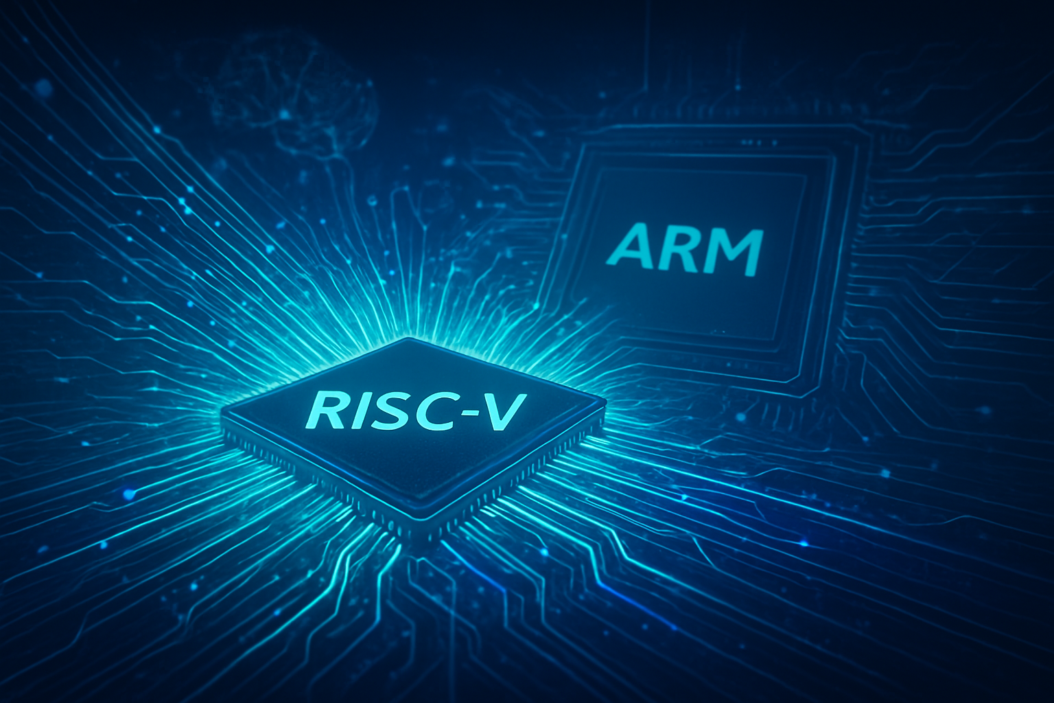
    The semiconductor industry is on the cusp of a significant shift as the open-standard RISC-V instruction set architecture (ISA) rapidly gains traction, presenting a formidable challenge to ARM's long-standing dominance in chip design. Developed at the University of California, Berkeley, and governed by the non-profit RISC-V International, this royalty-free and highly customizable architecture is democratizing processor design, fostering unprecedented innovation, and potentially reshaping the competitive landscape for silicon intellectual property. Its modularity, cost-effectiveness, and vendor independence are attracting a growing ecosystem of industry giants and nimble startups alike, heralding a new era where chip design is no longer exclusively the domain of proprietary giants.

    The immediate significance of RISC-V lies in its potential to dramatically lower barriers to entry for chip development, allowing companies to design highly specialized processors without incurring the hefty licensing fees associated with proprietary ISAs like ARM and x86. This open-source ethos is not only driving down costs but also empowering designers with unparalleled flexibility to tailor processors for specific applications, from tiny IoT devices to powerful AI accelerators and data center solutions. As geopolitical tensions highlight the need for independent and secure supply chains, RISC-V's neutral governance further enhances its appeal, positioning it as a strategic alternative for nations and corporations seeking autonomy in their technological infrastructure.

    A Technical Deep Dive into RISC-V's Architecture and AI Prowess

    At its core, RISC-V is a clean-slate, open-standard instruction set architecture (ISA) built upon Reduced Instruction Set Computer (RISC) principles, designed for simplicity, modularity, and extensibility. Unlike proprietary ISAs, its specifications are released under permissive open-source licenses, eliminating royalty payments—a stark contrast to ARM's per-chip royalty model. The architecture features a small, mandatory base integer ISA (RV32I, RV64I, RV128I) for general-purpose computing, which can be augmented by a range of optional standard extensions. These include M for integer multiply/divide, A for atomic operations, F and D for single and double-precision floating-point, C for compressed instructions to reduce code size, and crucially, V for vector operations, which are vital for high-performance computing and AI/ML workloads. This modularity allows chip designers to select only the necessary instruction groups, optimizing for power, performance, and silicon area.

    The true differentiator for RISC-V, particularly in the context of AI, lies in its unparalleled ability for custom extensions. Designers are free to define non-standard, application-specific instructions and accelerators without breaking compliance with the main RISC-V specification. This capability is a game-changer for AI/ML, enabling the direct integration of specialized hardware like Tensor Processing Units (TPUs), Graphics Processing Units (GPUs), or Neural Processing Units (NPUs) into the ISA. This level of customization allows for processors to be precisely tailored for specific AI algorithms, transformer workloads, and large language models (LLMs), offering an optimization potential that ARM's more fixed IP cores cannot match. While ARM has focused on evolving its instruction set over decades, RISC-V's fresh design avoids legacy complexities, promoting a more streamlined and efficient architecture.

    Initial reactions from the AI research community and industry experts have been overwhelmingly positive, recognizing RISC-V as an ideal platform for the future of AI/ML. Its modularity and extensibility are seen as perfectly suited for integrating custom AI accelerators, leading to highly efficient and performant solutions, especially at the edge. Experts note that RISC-V can offer significant advantages in computational performance per watt compared to ARM and x86, making it highly attractive for power-constrained edge AI devices and battery-operated solutions. The open nature of RISC-V also fosters a unified programming model across different processing units (CPU, GPU, NPU), simplifying development and accelerating time-to-market for AI solutions.

    Furthermore, RISC-V is democratizing AI hardware development, lowering the barriers to entry for smaller companies and academic institutions to innovate without proprietary constraints or prohibitive upfront costs. This is fostering local innovation globally, empowering a broader range of participants in the AI revolution. The rapid expansion of the RISC-V ecosystem, with major players like Alphabet (NASDAQ: GOOGL), Qualcomm (NASDAQ: QCOM), and Samsung (KRX: 005930) actively investing, underscores its growing viability. Forecasts predict substantial growth, particularly in the automotive sector for autonomous driving and ADAS, driven by AI applications. Even the design process itself is being revolutionized, with researchers demonstrating the use of AI to design a RISC-V CPU in under five hours, showcasing the synergistic potential between AI and the open-source architecture.

    Reshaping the Semiconductor Landscape: Impact on Tech Giants, AI Companies, and Startups

    The rise of RISC-V is sending ripples across the entire semiconductor industry, profoundly affecting tech giants, specialized AI companies, and burgeoning startups. Its open-source nature, flexibility, and cost-effectiveness are democratizing chip design and fostering a new era of innovation. AI companies, in particular, are at the forefront of this revolution, leveraging RISC-V's modularity to develop custom instructions and accelerators tailored for specific AI workloads. Companies like Tenstorrent are utilizing RISC-V in high-performance GPUs for training and inference of large neural networks, while Alibaba (NYSE: BABA) T-Head Semiconductor has released its XuanTie RISC-V series processors and an AI platform. Canaan Creative (NASDAQ: CAN) has also launched the world's first commercial edge AI chip based on RISC-V, demonstrating its immediate applicability in real-world AI systems.

    Tech giants are increasingly embracing RISC-V to diversify their IP portfolios, reduce reliance on proprietary architectures, and gain greater control over their hardware designs. Companies such as Alphabet (NASDAQ: GOOGL), MediaTek (TPE: 2454), NVIDIA (NASDAQ: NVDA), Intel (NASDAQ: INTC), Qualcomm (NASDAQ: QCOM), and NXP Semiconductors (NASDAQ: NXPI) are deeply committed to its development. NVIDIA, for instance, shipped an estimated 1 billion RISC-V cores in its GPUs in 2024. Qualcomm's acquisition of RISC-V server CPU startup Ventana Micro Systems underscores its strategic intent to boost CPU engineering and enhance its AI capabilities. Western Digital (NASDAQ: WDC) has integrated over 2 billion RISC-V cores into its storage devices, citing greater customization and reduced costs as key benefits. Even Meta Platforms (NASDAQ: META) is utilizing RISC-V for AI in its accelerator cards, signaling a broad industry shift towards open and customizable silicon.

    For startups, RISC-V represents a paradigm shift, significantly lowering the barriers to entry in chip design. The royalty-free nature of the ISA dramatically reduces development costs, sometimes by as much as 50%, enabling smaller companies to design, prototype, and manufacture their own specialized chips without the prohibitive licensing fees associated with ARM. This newfound freedom allows startups to focus on differentiation and value creation, carving out niche markets in IoT, edge computing, automotive, and security-focused devices. Notable RISC-V startups like SiFive, Axelera AI, Esperanto Technologies, and Rivos Inc. are actively developing custom CPU IP, AI accelerators, and high-performance system solutions for enterprise AI, proving that innovation is no longer solely the purview of established players.

    The competitive implications are profound. RISC-V breaks the vendor lock-in associated with proprietary ISAs, giving companies more choices and fostering accelerated innovation across the board. While the software ecosystem for RISC-V is still maturing compared to ARM and x86, major AI labs and tech companies are actively investing in developing and supporting the necessary tools and environments. This collective effort is propelling RISC-V into a strong market position, especially in areas where customization, cost-effectiveness, and strategic autonomy are paramount. Its ability to enable highly tailored processors for specific applications and workloads could lead to a proliferation of specialized chips, potentially disrupting markets previously dominated by standardized products and ushering in a more diverse and dynamic industry landscape.

    A New Era of Digital Sovereignty and Open Innovation

    The wider significance of RISC-V extends far beyond mere technical specifications, touching upon economic, innovation, and geopolitical spheres. Its open and royalty-free nature is fundamentally altering traditional cost structures, eliminating expensive licensing fees that previously acted as significant barriers to entry for chip design. This cost reduction, potentially as much as 50% for companies, is fostering a more competitive and innovative market, driving economic growth and creating job opportunities by enabling a diverse array of players to enter and specialize in the semiconductor market. Projections indicate a substantial increase in the RISC-V SoC market, with unit shipments potentially reaching 16.2 billion and revenues hitting $92 billion by 2030, underscoring its profound economic impact.

    In the broader AI landscape, RISC-V is perfectly positioned to accelerate current trends towards specialized hardware and edge computing. AI workloads, from low-power edge inference to high-performance large language models (LLMs) and data center training, demand highly tailored architectures. RISC-V's modularity allows developers to seamlessly integrate custom instructions and specialized accelerators like Neural Processing Units (NPUs) and tensor engines, optimizing for specific AI tasks such as matrix multiplications and attention mechanisms. This capability is revolutionizing AI development by providing an open ISA that enables a unified programming model across CPU, GPU, and NPU, simplifying coding, reducing errors, and accelerating development cycles, especially for the crucial domain of edge AI and IoT where power conservation is paramount.

    However, the path forward for RISC-V is not without its concerns. A primary challenge is the risk of fragmentation within its ecosystem. The freedom to create custom, non-standard extensions, while a strength, could lead to compatibility and interoperability issues between different RISC-V implementations. RISC-V International is actively working to mitigate this by encouraging standardization and community guidance for new extensions. Additionally, while the open architecture allows for public scrutiny and enhanced security, there's a theoretical risk of malicious actors introducing vulnerabilities. The maturity of the RISC-V software ecosystem also remains a point of concern, as it still plays catch-up with established proprietary architectures in terms of compiler optimization, broad application support, and significant presence in cloud computing.

    Comparing RISC-V's impact to previous technological milestones, it often draws parallels to the rise of Linux, which democratized software development and challenged proprietary operating systems. In the context of AI, RISC-V represents a paradigm shift in hardware development that mirrors how algorithmic and software breakthroughs previously defined AI milestones. Early AI advancements focused on novel algorithms, and later, open-source software frameworks like TensorFlow and PyTorch significantly accelerated development. RISC-V extends this democratization to the hardware layer, enabling the creation of highly specialized and efficient AI accelerators that can keep pace with rapidly evolving AI algorithms. It is not an AI algorithm itself, but a foundational hardware technology that provides the platform for future AI innovation, empowering innovators to tailor AI hardware precisely to evolving algorithmic demands, a feat not easily achievable with rigid proprietary architectures.

    The Horizon: From Edge AI to Data Centers and Beyond

    The trajectory for RISC-V in the coming years is one of aggressive expansion and increasing maturity across diverse applications. In the near term (1-3 years), significant progress is anticipated in bolstering its software ecosystem, with initiatives like the RISE Project accelerating the development of open-source software, including compilers, toolchains, and language runtimes. Key milestones in 2024 included the availability of Java v17, 21-24 runtimes and foundational Python packages, with 2025 focusing on hardware aligned with the recently ratified RVA23 Profile. This period will also see a surge in hardware IP development, with companies like Synopsys (NASDAQ: SNPS) transitioning existing CPU IP cores to RISC-V. The immediate impact will be felt most strongly in data centers and AI accelerators, where high-core-count designs and custom optimizations provide substantial benefits, alongside continued growth in IoT and edge computing.

    Looking further ahead, beyond three years, RISC-V aims for widespread market penetration and architectural leadership. A primary long-term objective is to achieve full ecosystem maturity, including comprehensive standardization of extensions and profiles to ensure compatibility and reduce fragmentation across implementations. Experts predict that the performance gap between high-end RISC-V and established architectures like ARM and x86 will effectively close by the end of 2026 or early 2027, enabling RISC-V to become the default architecture for new designs in IoT, edge computing, and specialized accelerators by 2030. The roadmap also includes advanced 5nm designs with chiplet-based architectures for disaggregated computing by 2028-2030, signifying its ambition to compete in the highest echelons of computing.

    The potential applications and use cases on the horizon are vast and varied. Beyond its strong foundation in embedded systems and IoT, RISC-V is perfectly suited for the burgeoning AI and machine learning markets, particularly at the edge, where its extensibility allows for specialized accelerators. The automotive sector is also rapidly embracing RISC-V for ADAS, self-driving cars, and infotainment, with projections suggesting that 25% of new automotive microcontrollers could be RISC-V-based by 2030. High-Performance Computing (HPC) and data centers represent another significant growth area, with data center deployments expected to have the highest growth trajectory, advancing at a 63.1% CAGR through 2030. Even consumer electronics, including smartphones and laptops, are on the radar, as RISC-V's customizable ISA allows for optimized power and performance.

    Despite this promising outlook, challenges remain. The ecosystem's maturity, particularly in software, needs continued investment to match the breadth and optimization of ARM and x86. Fragmentation, while being actively addressed by RISC-V International, remains a potential concern if not carefully managed. Achieving consistent performance and power efficiency parity with high-end proprietary cores for flagship devices is another hurdle. Furthermore, ensuring robust security features and addressing the skill gap in RISC-V development are crucial. Geopolitical factors, such as potential export control restrictions and the risk of divergent RISC-V versions due to national interests, also pose complex challenges that require careful navigation by the global community.

    Experts are largely optimistic, forecasting rapid market growth. The RISC-V SoC market, valued at $6.1 billion in 2023, is projected to soar to $92.7 billion by 2030, with a robust 47.4% CAGR. Overall RISC-V tech market is forecast to climb from $1.35 billion in 2025 to $8.16 billion by 2030. Shipments are expected to reach 16.2 billion units by 2030, with some research predicting a market share of almost 25% for RISC-V chips by the same year. The consensus is that AI will be a major driver, and the performance gap with ARM will close significantly. SiFive, a company founded by RISC-V's creators, asserts that RISC-V becoming the top ISA is "no longer a question of 'if' but 'when'," with many predicting it will secure the number two position behind ARM. The ongoing investments from tech giants and significant government funding underscore the growing confidence in RISC-V's potential to reshape the semiconductor industry, aiming to do for hardware what Linux did for operating systems.

    The Open Road Ahead: A Revolution Unfolding

    The rise of RISC-V marks a pivotal moment in the history of computing, representing a fundamental shift from proprietary, licensed architectures to an open, collaborative, and royalty-free paradigm. Key takeaways highlight its simplicity, modularity, and unparalleled customization capabilities, which allow for the precise tailoring of processors for diverse applications, from power-efficient IoT devices to high-performance AI accelerators. This open-source ethos is not only driving down development costs but also fostering an explosive ecosystem, with major tech giants like Alphabet (NASDAQ: GOOGL), Intel (NASDAQ: INTC), NVIDIA (NASDAQ: NVDA), Qualcomm (NASDAQ: QCOM), and Meta Platforms (NASDAQ: META) actively investing and integrating RISC-V into their strategic roadmaps.

    In the annals of AI history, RISC-V is poised to be a transformative force, enabling a new era of AI-native hardware design. Its inherent flexibility allows for the tight integration of specialized hardware like Neural Processing Units (NPUs) and custom tensor acceleration engines directly into the ISA, optimizing for specific AI workloads and significantly enhancing real-time AI responsiveness. This capability is crucial for the continued evolution of AI, particularly at the edge, where power efficiency and low latency are paramount. By breaking vendor lock-in, RISC-V empowers AI developers with the freedom to design custom processors and choose from a wider range of pre-developed AI chips, fostering greater innovation and creativity in AI/ML solutions and facilitating a unified programming model across heterogeneous processing units.

    The long-term impact of RISC-V is projected to be nothing short of revolutionary. Forecasts predict explosive market growth, with chip shipments of RISC-V-based units expected to reach a staggering 17 billion units by 2030, capturing nearly 25% of the processor market. The RISC-V system-on-chip (SoC) market, valued at $6.1 billion in 2023, is projected to surge to $92.7 billion by 2030. This growth will be significantly driven by demand in AI and automotive applications, leading many industry analysts to believe that RISC-V will eventually emerge as a dominant ISA, potentially surpassing existing proprietary architectures. It is poised to democratize advanced computing capabilities, much like Linux did for software, enabling smaller organizations and startups to develop cutting-edge solutions and establish robust technological infrastructure, while also influencing geopolitical and economic shifts by offering nations greater technological autonomy.

    In the coming weeks and months, several key developments warrant close observation. Google's official plans to support Android on RISC-V CPUs is a critical indicator, and further updates on developer tools and initial Android-compatible RISC-V devices will be keenly watched. The ongoing maturation of the software ecosystem, spearheaded by initiatives like the RISC-V Software Ecosystem (RISE) project, will be crucial for large-scale commercialization. Expect significant announcements from the automotive sector regarding RISC-V adoption in autonomous driving and ADAS. Furthermore, demonstrations of RISC-V's performance and stability in server and High-Performance Computing (HPC) environments, particularly from major cloud providers, will signal its readiness for mission-critical workloads. Finally, continued standardization progress by RISC-V International and the evolving geopolitical landscape surrounding this open standard will profoundly shape its trajectory, solidifying its position as a cornerstone for future innovation in the rapidly evolving world of artificial intelligence and beyond.


    This content is intended for informational purposes only and represents analysis of current AI developments.

    TokenRing AI delivers enterprise-grade solutions for multi-agent AI workflow orchestration, AI-powered development tools, and seamless remote collaboration platforms.
    For more information, visit https://www.tokenring.ai/.

  • Arteris Fortifies AI-Driven Future with Strategic Acquisition of Cycuity, Championing Semiconductor Cybersecurity

    Arteris Fortifies AI-Driven Future with Strategic Acquisition of Cycuity, Championing Semiconductor Cybersecurity

    SAN JOSE, CA – December 11, 2025 – In a pivotal move poised to redefine the landscape of semiconductor design and cybersecurity, Arteris, Inc. (NASDAQ: APLS), a leading provider of system IP for accelerating chiplet and System-on-Chip (SoC) creation, today announced its definitive agreement to acquire Cycuity, Inc., a pioneer in semiconductor cybersecurity assurance. This strategic acquisition, anticipated to close in Arteris' first fiscal quarter of 2026, signals a critical industry response to the escalating cyber threats targeting the very foundation of modern technology: the silicon itself.

    The integration of Cycuity's advanced hardware security verification solutions into Arteris's robust portfolio is a direct acknowledgment of the burgeoning importance of "secure by design" principles in an era increasingly dominated by complex AI systems and modular chiplet architectures. As the digital world grapples with a surge in hardware vulnerabilities—with the U.S. Department of Commerce's National Institute of Standards and Technology (NIST) reporting a staggering 15-fold increase in hardware-related Common Vulnerabilities and Exposures (CVEs) over the past five years—this acquisition positions Arteris at the forefront of building a more resilient and trustworthy silicon foundation for the AI-driven future.

    Unpacking the Technical Synergy: A "Shift-Left" in Hardware Security

    The core of this acquisition lies in the profound technical synergy between Cycuity's innovative Radix software and Arteris's established Network-on-Chip (NoC) interconnect IP. Cycuity's Radix is a sophisticated suite of software products meticulously engineered for hardware security verification. It empowers chip designers to identify and prevent exploits in SoC designs during the crucial pre-silicon stages, moving beyond traditional post-silicon security measures to embed security verification throughout the entire chip design lifecycle.

    Radix's capabilities are comprehensive, including static security analysis (Radix-ST) that performs deep analysis of Register Transfer Level (RTL) designs to pinpoint security issues early, mapping them to the MITRE Common Weakness Enumeration (CWE) database. This is complemented by dynamic security verification (Radix-S and Radix-M) for simulation and emulation, information flow analysis to visualize data paths, and quantifiable security coverage metrics. Crucially, Radix is designed to integrate seamlessly into existing Electronic Design Automation (EDA) tool workflows from industry giants like Cadence (NASDAQ: CDNS), Synopsys (NASDAQ: SNPS), and Siemens EDA.

    Arteris, on the other hand, is renowned for its FlexNoC® (non-coherent) and Ncore™ (cache-coherent) NoC interconnect IP, which provides the configurable, scalable, and low-latency on-chip communication backbone for data movement across SoCs and chiplets. The strategic integration means that security verification can now be applied directly to this interconnect fabric during the earliest design stages. This "shift-left" approach allows for the detection of vulnerabilities introduced during the integration of various IP blocks connected by the NoC, including those arising from unsecured interconnects, unprivileged access to sensitive data, and side-channel leakages. This proactive stance contrasts sharply with previous approaches that often treated security as a later-stage concern, leading to costly and difficult-to-patch vulnerabilities once silicon is fabricated. Initial reactions from industry experts, including praise from Mark Labbato, Senior Lead Engineer at Booz Allen Hamilton, underscore the value of Radix-ST's ability to enable early security analysis in verification cycles, reinforcing the "secure by design" principle.

    Reshaping the Competitive Landscape: Benefits and Disruptions

    The Arteris-Cycuity acquisition is poised to send ripples across the AI and broader tech industry, fundamentally altering competitive dynamics and market positioning. Companies involved in designing and utilizing advanced silicon for AI, autonomous systems, and data center infrastructure stand to benefit immensely. Arteris's existing customers, including major players like Advanced Micro Devices (NASDAQ: AMD), which already licenses Arteris's FlexGen NoC IP for its next-gen AI chiplet designs, will gain access to an integrated solution that ensures both efficient data movement and robust hardware security.

    This move strengthens Arteris's (NASDAQ: APLS) competitive position by offering a unique, integrated solution for secure on-chip data movement. It elevates the security standards for advanced SoCs and chiplets, potentially compelling other interconnect IP providers and major tech companies developing in-house silicon to invest more heavily in similar hardware security assurance. The main disruption will be a mandated "shift-left" in the security verification process, requiring closer collaboration between hardware design and security teams from the outset. While workflows might be enhanced, a complete overhaul is unlikely for companies already using compatible EDA tools, as Cycuity's Radix integrates seamlessly.

    The combined Arteris-Cycuity entity establishes a formidable market position, particularly in the burgeoning fields of AI and chiplet architectures. Arteris will offer a differentiated "secure by design" approach for on-chip data movement, providing a unique integrated offering of high-performance NoC IP with embedded hardware security assurance. This addresses a critical and growing industry need, particularly as Arteris positions itself as a leader in the transition to the chiplet era, where securing data movement within multi-die systems is paramount.

    Wider Significance: A New AI Milestone for Trustworthiness

    The Arteris-Cycuity acquisition transcends a typical corporate merger; it signifies a critical maturation point in the broader AI landscape. It underscores the industry's recognition that as AI becomes more powerful and pervasive, its trustworthiness hinges on the integrity of its foundational hardware. This development reflects several key trends: the explosion of hardware vulnerabilities, AI's double-edged sword in cybersecurity (both a tool for defense and offense), and the imperative of "secure by design."

    This acquisition doesn't represent a new algorithmic breakthrough or a dramatic increase in computational speed, like previous AI milestones such as IBM's Deep Blue or the advent of large language models. Instead, it marks a pivotal milestone in AI deployment and trustworthiness. While past breakthroughs asked, "What can AI do?" and "How fast can AI compute?", this acquisition addresses the increasingly vital question: "How securely and reliably can AI be built and deployed in the real world?"

    By focusing on hardware-level security, the combined entity directly tackles vulnerabilities that cannot be patched by software updates, such as microarchitectural side channels or logic bugs. This is especially crucial for chiplet-based designs, which introduce new security complexities at the die-to-die interface. While concerns about integration complexity and the performance/area overhead of comprehensive security measures exist, the long-term impact points towards a more resilient digital infrastructure and accelerated, more secure AI innovation, ultimately bolstering consumer confidence in advanced technologies.

    Future Horizons: Building the Secure AI Infrastructure

    In the near term, the combined Arteris-Cycuity entity will focus on the swift integration of Cycuity's Radix software into Arteris's NoC IP, aiming to deliver immediate enhancements for designers tackling complex SoCs and chiplets. This will empower engineers to detect and mitigate hardware vulnerabilities much earlier in the design cycle, reducing costly post-silicon fixes. In the long term, the acquisition is expected to solidify Arteris's leadership in multi-die solutions and AI accelerators, where secure and efficient integration across IP cores is paramount.

    Potential applications and use cases are vast, spanning AI and autonomous systems, where data integrity is critical for decision-making; the automotive industry, demanding robust hardware security for ADAS and autonomous driving; and the burgeoning Internet of Things (IoT) sector, which desperately needs a silicon-based hardware root of trust. Data centers and edge computing, heavily reliant on complex chiplet designs, will also benefit from enhanced protection against sophisticated threats.

    However, significant challenges remain in semiconductor cybersecurity. These include the relentless threat of intellectual property (IP) theft, the complexities of securing a global supply chain, the ongoing battle against advanced persistent threats (APTs), and the continuous need to balance security with performance and power efficiency. Experts predict significant growth in the global semiconductor manufacturing cybersecurity market, projected to reach US$6.4 billion by 2034, driven by the AI "giga cycle." This underscores the increasing emphasis on "secure by design" principles and integrated security solutions from design to production.

    Comprehensive Wrap-up: A Foundation for Trust

    Arteris's acquisition of Cycuity is more than just a corporate expansion; it's a strategic imperative in an age where the integrity of silicon directly impacts the trustworthiness of our digital world. The key takeaway is a proactive, "shift-left" approach to hardware security, embedding verification from the earliest design stages to counter the alarming rise in hardware vulnerabilities.

    This development marks a significant, albeit understated, milestone in AI history. It's not about what AI can do, but how securely and reliably it can be built and deployed. By fortifying the hardware foundation, Arteris and Cycuity are enabling greater confidence in AI systems for critical applications, from autonomous vehicles to national defense. The long-term impact promises a more resilient digital infrastructure, faster and more secure AI innovation, and ultimately, increased consumer trust in advanced technologies.

    In the coming weeks and months, industry observers will be watching closely for the official close of the acquisition, the seamless integration of Cycuity's technology into Arteris's product roadmap, and any new partnerships that emerge to further solidify this enhanced cybersecurity offering. The competitive landscape will likely react, potentially spurring further investments in hardware security across the IP and EDA sectors. This acquisition is a clear signal: in the era of AI and chiplets, hardware security is no longer an afterthought—it is the bedrock of innovation and trust.


    This content is intended for informational purposes only and represents analysis of current AI developments.

    TokenRing AI delivers enterprise-grade solutions for multi-agent AI workflow orchestration, AI-powered development tools, and seamless remote collaboration platforms.
    For more information, visit https://www.tokenring.ai/.

  • Broadcom Soars: AI Dominance Fuels Investor Optimism and Skyrocketing Price Targets Ahead of Earnings

    Broadcom Soars: AI Dominance Fuels Investor Optimism and Skyrocketing Price Targets Ahead of Earnings

    Broadcom (NASDAQ: AVGO) is currently riding a wave of unprecedented investor optimism, with its stock performance surging and analyst price targets climbing to new heights as the company approaches its Q4 fiscal year 2025 earnings announcement on December 11, 2025. This robust market confidence is largely a testament to Broadcom's strategic positioning at the epicenter of the artificial intelligence (AI) revolution, particularly its critical role in supplying advanced chips and networking solutions to hyperscale data centers. The semiconductor giant's impressive trajectory is not just a win for its shareholders but also serves as a significant bellwether for the broader semiconductor market, highlighting the insatiable demand for AI infrastructure.

    The fervor surrounding Broadcom stems from its deep entrenchment in the AI ecosystem, where its custom silicon, AI accelerators, and high-speed networking chips are indispensable for powering the next generation of AI models and applications. Analysts are projecting substantial year-over-year growth in both earnings per share and revenue for Q4 2025, underscoring the company's strong execution and market leadership. This bullish sentiment, however, also places immense pressure on Broadcom to not only meet but significantly exceed these elevated expectations to justify its premium valuation and sustain its remarkable market momentum.

    The AI Engine: Unpacking Broadcom's Technical Edge and Market Impact

    Broadcom's stellar performance is deeply rooted in its sophisticated technical contributions to the AI and data center landscape. The company has become an indispensable hardware supplier for the world's leading hyperscalers, who are aggressively building out their AI infrastructure. A significant portion of Broadcom's growth is driven by the surging demand for its AI accelerators, custom silicon (ASICs and XPUs), and cutting-edge networking chips, with its AI semiconductor segment projected to hit $6.2 billion in Q4 2025, marking an astounding 66% year-over-year increase.

    At the heart of Broadcom's technical prowess are its key partnerships and product innovations. The company is the designer and manufacturer of Google's Tensor Processing Units (TPUs), which were instrumental in training Google's advanced Gemini 3 model. The anticipated growth in TPU demand, potentially reaching 4.5-5 million units by 2026, solidifies Broadcom's foundational role in AI development. Furthermore, a monumental 10-gigawatt AI accelerator and networking deal with OpenAI, valued at over $100 billion in lifetime revenue, underscores the company's critical importance to the leading edge of AI research. Broadcom is also reportedly engaged in developing custom chips for Microsoft and is benefiting from increased AI workloads at tech giants like Meta, Apple, and Anthropic. Its new products, such as the Thor Ultra 800G AI Ethernet Network Interface Card (NIC) and Tomahawk 6 networking chips, are designed to handle the immense data throughput required by modern AI applications, further cementing its technical leadership.

    This differentiated approach, focusing on highly specialized custom silicon and high-performance networking, sets Broadcom apart from many competitors. While other companies offer general-purpose GPUs, Broadcom's emphasis on custom ASICs allows for optimized performance and power efficiency tailored to specific AI workloads of its hyperscale clients. This deep integration and customization create significant barriers to entry for rivals and foster long-term partnerships. Initial reactions from the AI research community and industry experts have highlighted Broadcom's strategic foresight in anticipating and addressing the complex hardware needs of large-scale AI deployment, positioning it as a foundational enabler of the AI era.

    Reshaping the Semiconductor Landscape: Competitive Implications and Strategic Advantages

    Broadcom's current trajectory has profound implications for AI companies, tech giants, and startups across the industry. Clearly, the hyperscalers and AI innovators who partner with Broadcom for their custom silicon and networking needs stand to benefit directly from its advanced technology, enabling them to build more powerful and efficient AI infrastructure. This includes major players like Google, OpenAI, Microsoft, Meta, Apple, and Anthropic, whose AI ambitions are increasingly reliant on Broadcom's specialized hardware.

    The competitive landscape within the semiconductor industry is being significantly reshaped by Broadcom's strategic moves. Its robust position in custom AI accelerators and high-speed networking chips provides a formidable competitive advantage, particularly against companies that may offer more generalized solutions. While NVIDIA (NASDAQ: NVDA) remains a dominant force in general-purpose AI GPUs, Broadcom's expertise in custom ASICs and network infrastructure positions it as a complementary, yet equally critical, player in the overall AI hardware stack. This specialization allows Broadcom to capture a unique segment of the market, focusing on bespoke solutions for the largest AI developers.

    Furthermore, Broadcom's strategic acquisition of VMware in 2023 has significantly bolstered its infrastructure software segment, transforming its business model and strengthening its recurring revenue streams. This diversification into high-margin software services, projected to grow by 15% year-over-year to $6.7 billion, provides a stable revenue base that complements its cyclical hardware business. This dual-pronged approach offers a significant strategic advantage, allowing Broadcom to offer comprehensive solutions that span both hardware and software, potentially disrupting existing product or service offerings from companies focused solely on one aspect. This integrated strategy enhances its market positioning, making it a more attractive partner for enterprises seeking end-to-end infrastructure solutions for their AI and cloud initiatives.

    Broadcom's Role in the Broader AI Landscape: Trends, Impacts, and Concerns

    Broadcom's current market performance and strategic focus firmly embed it within the broader AI landscape and key technological trends. Its emphasis on custom AI accelerators and high-speed networking aligns perfectly with the industry's shift towards more specialized and efficient hardware for AI workloads. As AI models grow in complexity and size, the demand for purpose-built silicon that can offer superior performance per watt and lower latency becomes paramount. Broadcom's offerings directly address this critical need, driving the efficiency and scalability of AI data centers.

    The impact of Broadcom's success extends beyond just its financial statements. It signifies a maturation in the AI hardware market, where custom solutions are becoming increasingly vital for competitive advantage. This trend could accelerate the development of more diverse AI hardware architectures, moving beyond a sole reliance on GPUs for all AI tasks. Broadcom's collaboration with hyperscalers on custom chips also highlights the increasing vertical integration within the tech industry, where major cloud providers are looking to tailor hardware specifically for their internal AI frameworks.

    However, this rapid growth and high valuation also bring potential concerns. Broadcom's current forward price-to-earnings (P/E) ratio of 45x and a trailing P/E of 96x are elevated, suggesting that the company needs to consistently deliver "significant beats" on earnings to maintain investor confidence and avoid a potential stock correction. There are also challenges in the non-AI semiconductor segment and potential gross margin pressures due to the evolving product mix, particularly the shift toward custom accelerators. Supply constraints, potentially due to competition with NVIDIA for critical components like wafers, packaging, and memory, could also hinder Broadcom's ambitious growth targets. The possibility of major tech companies cutting their AI capital expenditure budgets in 2026, while currently viewed as remote, presents a macro-economic risk that could impact Broadcom's long-term revenue streams. This situation draws comparisons to past tech booms, where high valuations were often met with significant corrections if growth expectations were not met, underscoring the delicate balance between innovation, market demand, and investor expectations.

    The Road Ahead: Future Developments and Expert Predictions

    Looking ahead, Broadcom's near-term future is largely tied to the continued explosive growth of AI infrastructure and its ability to execute on its current projects and partnerships. In the immediate future, the market will keenly watch its Q4 2025 earnings announcement on December 11, 2025, for confirmation of the strong growth projections and any updates on its AI pipeline. Continued strong demand for Google's TPUs and the successful progression of the OpenAI deal will be critical indicators. Experts predict that Broadcom will further deepen its relationships with hyperscalers, potentially securing more custom chip design wins as these tech giants seek greater control and optimization over their AI hardware stacks.

    In the long term, Broadcom is expected to continue innovating in high-speed networking and custom silicon, pushing the boundaries of what's possible in AI data centers. Potential applications and use cases on the horizon include more advanced AI accelerators for specific modalities like generative AI, further integration of optical networking for even higher bandwidth, and potentially expanding its custom silicon offerings to a broader range of enterprise AI applications beyond just hyperscalers. The full integration and synergy benefits from the VMware acquisition will also become more apparent, potentially leading to new integrated hardware-software solutions for hybrid cloud and edge AI deployments.

    However, several challenges need to be addressed. Managing supply chain constraints amidst intense competition for manufacturing capacity will be crucial. Maintaining high gross margins as the product mix shifts towards custom, often lower-margin, accelerators will require careful financial management. Furthermore, the evolving landscape of AI chip architecture, with new players and technologies constantly emerging, demands continuous innovation to stay ahead. Experts predict that the market for AI hardware will become even more fragmented and specialized, requiring companies like Broadcom to remain agile and responsive to changing customer needs. The ability to navigate geopolitical tensions and maintain access to critical manufacturing capabilities will also be a significant factor in its sustained success.

    A Defining Moment for Broadcom and the AI Era

    Broadcom's current market momentum represents a significant milestone, not just for the company but for the broader AI industry. The key takeaways are clear: Broadcom has strategically positioned itself as an indispensable enabler of the AI revolution through its leadership in custom AI silicon and high-speed networking. Its strong financial performance and overwhelming investor optimism underscore the critical importance of specialized hardware in building the next generation of AI infrastructure. The successful integration of VMware also highlights a savvy diversification strategy, providing a stable software revenue base alongside its high-growth hardware segments.

    This development's significance in AI history cannot be overstated. It underscores the fact that while software models capture headlines, the underlying hardware infrastructure is just as vital, if not more so, for the actual deployment and scaling of AI. Broadcom's story is a testament to the power of deep technical expertise and strategic partnerships in a rapidly evolving technological landscape. It also serves as a critical indicator of the massive capital expenditures being poured into AI by the world's largest tech companies.

    Looking ahead, the coming weeks and months will be crucial. All eyes will be on Broadcom's Q4 earnings report for confirmation of its strong growth trajectory and any forward-looking statements that could further shape investor sentiment. Beyond earnings, watch for continued announcements regarding new custom chip designs, expanded partnerships with AI innovators, and further synergistic developments from the VMware integration. The semiconductor market, particularly the AI hardware segment, remains dynamic, and Broadcom's performance will offer valuable insights into the health and direction of this transformative industry.


    This content is intended for informational purposes only and represents analysis of current AI developments.

    TokenRing AI delivers enterprise-grade solutions for multi-agent AI workflow orchestration, AI-powered development tools, and seamless remote collaboration platforms.
    For more information, visit https://www.tokenring.ai/.

  • ACM Research Inc. Gears Up for 14th Annual NYC Summit 2025: A Strategic Play for Semiconductor Dominance

    ACM Research Inc. Gears Up for 14th Annual NYC Summit 2025: A Strategic Play for Semiconductor Dominance

    New York, NY – December 1, 2025 – ACM Research Inc. (NASDAQ: ACMR), a global leader in advanced wafer and panel processing solutions, is poised to make a significant impact at the upcoming 14th Annual NYC Summit, scheduled for December 16, 2025. This highly anticipated invite-only investor conference will serve as a pivotal platform for ACM Research to amplify its industry visibility, cultivate new strategic partnerships, and solidify its commanding position within the rapidly evolving semiconductor manufacturing landscape. The company's participation underscores the critical importance of direct engagement with the financial community and industry leaders for specialized equipment suppliers in today's dynamic tech environment.

    The summit presents a crucial opportunity for ACM Research to showcase its latest innovations and articulate its growth trajectory to a discerning audience of global tech, startup, and venture leaders. As the semiconductor industry continues its relentless drive towards miniaturization and higher performance, the role of advanced processing solutions becomes ever more critical. ACM Research's strategic presence at such a high-profile event highlights its commitment to maintaining technological leadership and expanding its global footprint.

    Pushing the Boundaries of Wafer and Panel Processing

    ACM Research Inc. has distinguished itself through its comprehensive suite of wet processing and plating tools, which are indispensable for next-generation chiplet integration and advanced packaging applications. Their technological prowess is evident in their key offerings, which include sophisticated wet cleaning equipment such as the Ultra C SAPS II and V, Ultra C TEBO II and V, and the Ultra-C Tahoe wafer cleaning tools. These systems are engineered for front-end production processes, delivering unparalleled defect removal and enabling advanced cleaning protocols with significantly reduced chemical consumption, thereby addressing both performance and environmental considerations.

    Beyond traditional wafer processing, ACM Research is at the vanguard of innovation in advanced packaging. The company's portfolio extends to a range of specialized tools including coaters, developers, photoresist strippers, scrubbers, wet etchers, and copper-plating tools. A particular area of focus and differentiation lies in their contributions to panel-level packaging (PLP). ACM Research's new Ultra ECP ap-p Horizontal Plating tool, Ultra C vac-p Flux Cleaning tool, and Ultra C bev-p Bevel Etching Tool are revolutionary, offering the capability to achieve sub-micron features on square panels. This advancement is especially crucial for the burgeoning demands of AI chip manufacturing, including high-performance GPUs and high-density high bandwidth memory (HBM), where precision and efficiency are paramount. These innovations set ACM Research apart by providing solutions that are not only technically superior but also directly address the most pressing needs of advanced semiconductor fabrication. Initial reactions from the industry experts suggest that ACM Research's continuous innovation in these critical areas positions them as a key enabler for the next generation of AI and high-performance computing hardware.

    Strategic Implications for the Semiconductor Ecosystem

    ACM Research Inc.'s robust participation in events like the NYC Summit carries significant implications for AI companies, tech giants, and burgeoning startups across the semiconductor value chain. Companies heavily invested in AI development, such as Nvidia (NASDAQ: NVDA), Intel (NASDAQ: INTC), and AMD (NASDAQ: AMD), which rely on cutting-edge chip manufacturing, stand to directly benefit from ACM Research's advancements. Their ability to provide superior wafer and panel processing solutions directly impacts the efficiency, yield, and ultimately, the cost of producing the complex chips that power AI.

    The competitive landscape for semiconductor equipment suppliers is intense, with major players like Applied Materials (NASDAQ: AMAT) and Lam Research (NASDAQ: LRCX) vying for market share. ACM Research's consistent innovation and strategic visibility at investor conferences help them to carve out and expand their niche, particularly in specialized wet processing and advanced packaging. Their focus on areas like panel-level packaging for AI chips offers a distinct competitive advantage, potentially disrupting existing product lines that may not be as optimized for these emerging requirements. By showcasing their technological edge and financial performance, ACM Research strengthens its market positioning, making it an increasingly attractive partner for chip manufacturers looking to future-proof their production capabilities. This strategic advantage allows them to influence design choices and manufacturing processes, further embedding their solutions into the core of next-generation semiconductor fabrication.

    Broader Significance and Industry Trends

    ACM Research's engagement at the NYC Summit highlights a broader trend within the semiconductor industry: the increasing importance of specialized equipment suppliers in driving innovation. As chip designs become more intricate and manufacturing processes more demanding, the expertise of companies like ACM Research becomes indispensable. Their advancements in wet processing and advanced packaging directly contribute to overcoming fundamental physical limitations in chip design and production, fitting perfectly into the overarching industry trend towards heterogeneous integration and chiplet architectures.

    The impact extends beyond mere technical capabilities. High industry visibility for specialized suppliers is critical for attracting the necessary capital for continuous R&D, fostering strategic collaborations, and navigating complex global supply chains. In an era marked by geopolitical shifts and an intensified focus on semiconductor independence, strong partnerships between equipment suppliers and chip manufacturers are vital for bolstering national technological capabilities and supply chain resilience. Potential concerns, however, include the intense capital expenditure required for R&D in this sector and the rapid pace of technological obsolescence. Compared to previous AI milestones, where breakthroughs often focused on algorithms or software, the current emphasis on hardware enablers like those provided by ACM Research signifies a maturing industry where physical limitations are now a primary bottleneck for further AI advancement.

    Envisioning Future Developments

    Looking ahead, the semiconductor industry is on the cusp of transformative changes, with AI, IoT, and autonomous vehicles driving unprecedented demand for advanced chips. ACM Research is well-positioned to capitalize on these trends. Near-term developments are likely to see continued refinement and expansion of their existing wet processing and advanced packaging solutions, with an emphasis on even greater precision, efficiency, and sustainability. The company's ongoing expansion, including the development of an R&D facility in Oregon, signals a commitment to accelerating new customer initiatives and pushing the boundaries of what's possible in semiconductor manufacturing.

    Longer-term, experts predict a growing reliance on novel materials and manufacturing techniques to overcome the limitations of silicon. ACM Research's expertise in wet processing could prove crucial in adapting to these new material science challenges. Potential applications and use cases on the horizon include ultra-low power AI accelerators, neuromorphic computing hardware, and advanced quantum computing components, all of which will demand highly specialized and precise fabrication processes. Challenges that need to be addressed include the escalating costs of developing next-generation tools, the need for a highly skilled workforce, and navigating intellectual property landscapes. Experts predict that companies like ACM Research, which can innovate rapidly and form strong strategic alliances, will be the key architects of the future digital economy.

    A Crucial Juncture for Semiconductor Innovation

    ACM Research Inc.'s participation in the 14th Annual NYC Summit 2025 is more than just a corporate appearance; it's a strategic declaration of intent and a testament to the company's pivotal role in the global semiconductor ecosystem. The key takeaway is the undeniable importance of specialized equipment suppliers in driving the fundamental advancements that underpin the entire tech industry, particularly the explosive growth of artificial intelligence. By showcasing their cutting-edge wafer and panel processing solutions, ACM Research reinforces its position as an indispensable partner for chip manufacturers navigating the complexities of next-generation fabrication.

    This development holds significant historical importance in AI, as it underscores the shift from purely software-driven innovation to a renewed focus on hardware enablement as a bottleneck and a critical area for breakthrough. The ability to produce more powerful, efficient, and cost-effective AI chips hinges directly on the capabilities provided by companies like ACM Research. The long-term impact will be felt across all sectors reliant on advanced computing, from data centers to consumer electronics. In the coming weeks and months, industry watchers should closely monitor the partnerships and investment announcements stemming from the NYC Summit, as these will likely shape the trajectory of semiconductor manufacturing and, by extension, the future of AI.


    This content is intended for informational purposes only and represents analysis of current AI developments.

    TokenRing AI delivers enterprise-grade solutions for multi-agent AI workflow orchestration, AI-powered development tools, and seamless remote collaboration platforms.
    For more information, visit https://www.tokenring.ai/.

  • Insider Exodus: Navitas Semiconductor Director Dumps $12.78 Million in Stock Amidst Market Jitters

    Insider Exodus: Navitas Semiconductor Director Dumps $12.78 Million in Stock Amidst Market Jitters

    December 1, 2025 – A significant wave of insider selling has cast a shadow over Navitas Semiconductor (NASDAQ:NVTS), a prominent player in the gallium nitride (GaN) power IC market. On June 11, 2025, company director Brian Long initiated a substantial divestment, filing to sell 1.5 million shares of common stock valued at approximately $12.78 million. This move, part of a broader pattern of insider transactions throughout mid-2025, has ignited discussions among investors about the potential implications for the company's future performance and overall market confidence.

    The substantial sale by a key director, particularly when coupled with other insider divestments, often serves as a critical signal for the market. While insider sales can be driven by a variety of personal financial motivations, the sheer volume and timing of these transactions at Navitas Semiconductor, especially after a period of significant stock appreciation, have raised questions about whether those closest to the company perceive its current valuation as unsustainable or anticipate headwinds on the horizon.

    Unpacking the $12.78 Million Divestment and Broader Insider Trends

    The $12.78 million stock sale by Brian Long on June 11, 2025, was not an isolated incident but rather a prominent event within a larger trend of insider selling at Navitas Semiconductor. Mr. Long, a director at the company, has significantly reduced his holdings, with total share divestments amounting to approximately $19.87 million since March 21, 2025, including additional sales of 455,596 shares for $2.75 million in September 2025 and 1,247,700 shares for $7.25 million just days prior. This pattern suggests a sustained effort by the director to monetize his stake.

    Beyond Mr. Long, other Navitas directors and executives, including Ranbir Singh, Gary Kent Wunderlich Jr., Richard J. Hendrix, and CFO Todd Glickman, have also participated in selling activities. Collectively, net insider selling within a 90-day period ending around late September/early October 2025 totaled approximately $13.1 million, with Mr. Long's transactions being the primary driver. This "cluster selling" pattern, where multiple insiders sell around the same time, is often viewed with greater concern by market analysts than isolated transactions.

    While no explicit public statement was made by Brian Long regarding the specific $12.78 million sale, common rationales for such large insider divestments in the semiconductor sector include profit-taking after substantial stock appreciation—Navitas shares had surged over 140% in the year leading up to September 2025 and 170.3% year-to-date as of November 2025. Other potential reasons include a belief in potential overvaluation, with Navitas sporting a price-to-sales (P/S) ratio of 30.04 in November 2025, or routine portfolio management and diversification strategies, often conducted through pre-established Rule 10b5-1 trading plans. However, the volume and frequency of these sales have fueled speculation that insiders might be locking in gains amidst concerns about future growth or current valuation.

    Implications for Navitas Semiconductor and the Broader AI/Semiconductor Landscape

    The significant insider selling at Navitas Semiconductor (NASDAQ:NVTS) carries notable implications for the company itself, its competitive standing, and investor sentiment across the broader AI and semiconductor industries. For Navitas, the immediate aftermath of these sales, coupled with disappointing financial results, has been challenging. The stock experienced a sharp 21.7% plunge following its Q3 2025 earnings report, which revealed "sluggish performance and a tepid outlook." This decline occurred despite the stock's robust year-to-date performance, suggesting that the insider selling contributed to an underlying investor apprehension that was exacerbated by negative news.

    Companies like Navitas, operating in the high-growth but capital-intensive semiconductor sector, rely heavily on investor confidence to fuel their expansion and innovation. Large-scale insider divestments, particularly when multiple executives are involved, can erode this confidence. Investors often interpret such moves as a lack of faith in the company's future prospects or a signal that the stock is overvalued. This can lead to increased market scrutiny, downward pressure on the stock price, and potentially impact the company's ability to raise capital or make strategic acquisitions on favorable terms. The company's reported net income loss of $49.1 million for the quarter ending June 2025 and negative operating cash flow further underscore "ongoing operating challenges" that, when combined with insider selling, present a concerning picture.

    In the competitive landscape of AI-driven semiconductors, where innovation and market perception are paramount, any signal of internal doubt can be detrimental. While Navitas focuses on GaN power ICs, a critical component for efficient power conversion in various AI and data center applications, sustained insider selling could affect its market positioning relative to larger, more diversified tech giants or even other agile startups in the power electronics space. It could also influence analysts' ratings and institutional investor interest, potentially disrupting future growth trajectories or strategic partnerships crucial for long-term success.

    Wider Significance in the Broader AI Landscape and Market Trends

    The insider selling at Navitas Semiconductor (NASDAQ:NVTS) fits into a broader narrative within the AI and technology sectors, highlighting the often-complex interplay between rapid innovation, soaring valuations, and the pragmatic decisions of those at the helm. In an era where AI advancements are driving unprecedented market enthusiasm and pushing valuations to historic highs, the semiconductor industry, as the foundational technology provider, has been a significant beneficiary. However, this also brings increased scrutiny on sustainability and potential bubbles.

    The events at Navitas serve as a cautionary tale within this landscape. While the company's technology is relevant to the power efficiency demands of AI, the insider sales, coinciding with a period of "dreary profit indicators" and "weak fundamentals," underscore the importance of distinguishing between technological promise and financial performance. This situation could prompt investors to more critically evaluate other high-flying AI-related semiconductor stocks, looking beyond hype to fundamental metrics and insider confidence.

    Historically, periods of significant insider selling have often preceded market corrections or slower growth phases for individual companies. While not always a definitive predictor, such activity can act as a "red flag," especially when multiple insiders are selling. This scenario draws comparisons to past tech booms where early investors or executives cashed out at peak valuations, leaving retail investors to bear the brunt of subsequent downturns. The current environment, with its intense focus on AI's transformative potential, makes such insider signals particularly potent, potentially influencing broader market sentiment and investment strategies across the tech sector.

    Exploring Future Developments and Market Outlook

    Looking ahead, the implications of the insider selling at Navitas Semiconductor (NASDAQ:NVTS) are likely to continue influencing investor behavior and market perceptions in the near and long term. In the immediate future, market participants will be closely watching Navitas's subsequent earnings reports and any further insider transaction disclosures. A sustained pattern of insider selling, particularly if coupled with continued "sluggish performance," could further depress the stock price and make it challenging for the company to regain investor confidence. Conversely, a significant shift towards insider buying or a dramatic improvement in financial results could help alleviate current concerns.

    Potential applications and use cases for Navitas's GaN technology remain strong, particularly in areas demanding high power efficiency like AI data centers, electric vehicles, and fast charging solutions. However, the company needs to demonstrate robust execution and translate technological promise into consistent profitability. Challenges that need to be addressed include improving operating cash flow, narrowing net income losses, and clearly articulating a path to sustained profitability amidst intense competition and the cyclical nature of the semiconductor industry.

    Experts predict that the market will continue to differentiate between companies with strong fundamentals and those whose valuations are primarily driven by speculative enthusiasm. For Navitas, the coming months will be crucial in demonstrating its ability to navigate these challenges. What happens next will likely depend on whether the company can deliver on its growth promises, whether insider sentiment shifts, and how the broader semiconductor market reacts to ongoing economic conditions and AI-driven demand.

    Comprehensive Wrap-Up: A Bellwether for Investor Prudence

    The substantial insider stock sale by Director Brian Long at Navitas Semiconductor (NASDAQ:NVTS) in mid-2025, alongside a pattern of broader insider divestments, serves as a significant event for investors to consider. The key takeaway is that while insider sales can be for personal reasons, the volume and timing of these transactions, especially in a company that subsequently reported "sluggish performance and a tepid outlook," often signal a lack of confidence or a belief in overvaluation from those with the most intimate company knowledge.

    This development holds considerable significance in the current AI-driven market, where valuations in the semiconductor sector have soared. It underscores the critical need for investors to look beyond the hype and scrutinize fundamental financial health and insider sentiment. The 21.7% plunge in Navitas's stock after its Q3 2025 results, against a backdrop of ongoing insider selling and "weak fundamentals," highlights how quickly market sentiment can turn when internal signals align with disappointing financial performance.

    In the long term, the Navitas situation could become a case study for investor prudence in rapidly expanding tech sectors. What to watch for in the coming weeks and months includes further insider transaction disclosures, the company's ability to improve its financial performance, and how the market's perception of "AI-adjacent" stocks evolves. The balance between technological innovation and robust financial fundamentals will undoubtedly remain a key determinant of success.


    This content is intended for informational purposes only and represents analysis of current AI developments.

    TokenRing AI delivers enterprise-grade solutions for multi-agent AI workflow orchestration, AI-powered development tools, and seamless remote collaboration platforms.
    For more information, visit https://www.tokenring.ai/.

  • South Korea’s Semiconductor Giants Face Mounting Carbon Risks Amid Global Green Shift

    South Korea’s Semiconductor Giants Face Mounting Carbon Risks Amid Global Green Shift

    The global semiconductor industry, a critical enabler of artificial intelligence and advanced technology, is increasingly under pressure to decarbonize its operations and supply chains. A recent report by the Institute for Energy Economics and Financial Analysis (IEEFA) casts a stark spotlight on South Korea, revealing that the nation's leading semiconductor manufacturers, Samsung (KRX:005930) and SK Hynix (KRX:000660), face significant and escalating carbon risks. This vulnerability stems primarily from South Korea's sluggish adoption of renewable energy and the rapid tightening of international carbon regulations, threatening the competitiveness and future growth of these tech titans in an AI-driven world.

    The IEEFA's findings underscore a critical juncture for South Korea, a global powerhouse in chip manufacturing. As the world shifts towards a greener economy, the report, titled "Navigating supply chain carbon risks in South Korea," serves as a potent warning: failure to accelerate renewable energy integration and manage Scope 2 and 3 emissions could lead to substantial financial penalties, loss of market share, and reputational damage. This situation has immediate significance for the entire tech ecosystem, from AI developers relying on cutting-edge silicon to consumers demanding sustainably produced electronics.

    The Carbon Footprint Challenge: A Deep Dive into South Korea's Semiconductor Emissions

    The IEEFA report meticulously details the specific carbon challenges confronting South Korea's semiconductor sector. A core issue is the nation's ambitious yet slow-moving renewable energy targets. South Korea's 11th Basic Plan for Long-Term Electricity Supply and Demand (BPLE) projects renewable electricity to constitute only 21.6% of the power mix by 2030 and 32.9% by 2038. This trajectory places South Korea at least 15 years behind global peers in achieving a 30% renewable electricity threshold, a significant lag when the world average stands at 30.25%. The continued reliance on fossil fuels, particularly liquefied natural gas (LNG), and speculative nuclear generation, is identified as a high-risk strategy that will inevitably lead to increased carbon costs.

    The carbon intensity of South Korean chipmakers is particularly alarming. Samsung Device Solutions (DS) recorded approximately 41 million tonnes of carbon dioxide equivalent (tCO2e) in Scope 1–3 emissions in 2024, making it the highest among seven major global tech companies analyzed by IEEFA. Its carbon intensity is a staggering 539 tCO2e per USD million of revenue, dramatically higher than global tech purchasers like Apple (37 tCO2e/USD million), Google (67 tCO2e/USD million), and Amazon Web Services (107 tCO2e/USD million). This disparity points to inadequate clean energy use and insufficient upstream supply chain GHG management. Similarly, SK Hynix exhibits a high carbon intensity of around 246 tCO2e/USD million. Despite being an RE100 member, its current 30% renewable energy achievement falls short of the global average for RE100 members, and plans for LNG-fired power plants for new facilities further complicate its sustainability goals.

    These figures highlight a fundamental difference from approaches taken by competitors in other regions. While many global semiconductor players and their customers are aggressively pursuing 100% renewable energy goals and demanding comprehensive Scope 3 emissions reporting, South Korea's energy policy and corporate actions appear to be lagging. The initial reactions from environmental groups and sustainability-focused investors emphasize the urgency for South Korean policymakers and industry leaders to recalibrate their strategies to align with global decarbonization efforts, or risk significant economic repercussions.

    Competitive Implications for AI Companies, Tech Giants, and Startups

    The mounting carbon risks in South Korea carry profound implications for the global AI ecosystem, impacting established tech giants and nascent startups alike. Companies like Samsung and SK Hynix, crucial suppliers of memory chips and logic components that power AI servers, edge devices, and large language models, stand to face significant competitive disadvantages. Increased carbon costs, stemming from South Korea's Emissions Trading Scheme (ETS) and potential future inclusion in mechanisms like the EU's Carbon Border Adjustment Mechanism (CBAM), could erode profit margins. For instance, Samsung DS could see carbon costs escalate from an estimated USD 26 million to USD 264 million if free allowances are eliminated, directly impacting their ability to invest in next-generation AI technologies.

    Beyond direct costs, the carbon intensity of South Korean semiconductor production poses a substantial risk to market positioning. Global tech giants and major AI labs, increasingly committed to their own net-zero targets, are scrutinizing their supply chains for lower-carbon suppliers. U.S. fabless customers, who represent a significant portion of South Korea's semiconductor exports, are already prioritizing manufacturers using renewable energy. If Samsung and SK Hynix fail to accelerate their renewable energy adoption, they risk losing contracts and market share to competitors like Taiwan Semiconductor Manufacturing Company (TSMC) (NYSE:TSM), which has set more aggressive RE100 targets. This could disrupt the supply of critical AI hardware components, forcing AI companies to re-evaluate their sourcing strategies and potentially absorb higher costs from greener, albeit possibly more expensive, alternatives.

    The investment landscape is also shifting dramatically. Global investors are increasingly divesting from carbon-intensive industries, which could raise financing costs for South Korean manufacturers seeking capital for expansion or R&D. Startups in the AI hardware space, particularly those focused on energy-efficient AI or sustainable computing, might find opportunities to differentiate themselves by partnering with or developing solutions that minimize carbon footprints. However, the overall competitive implications suggest a challenging road ahead for South Korean chipmakers unless they make a decisive pivot towards a greener supply chain, potentially disrupting existing product lines and forcing strategic realignments across the entire AI value chain.

    Wider Significance: A Bellwether for Global Supply Chain Sustainability

    The challenges faced by South Korea's semiconductor industry are not isolated; they are a critical bellwether for broader AI landscape trends and global supply chain sustainability. As AI proliferates, the energy demands of data centers, training large language models, and powering edge AI devices are skyrocketing. This places immense pressure on the underlying hardware manufacturers to prove their environmental bona fides. The IEEFA report underscores a global shift where Environmental, Social, and Governance (ESG) factors are no longer peripheral but central to investment decisions, customer preferences, and regulatory compliance.

    The implications extend beyond direct emissions. The growing demand for comprehensive Scope 1, 2, and 3 GHG emissions reporting, driven by regulations like IFRS S2, forces companies to trace and report emissions across their entire value chain—from raw material extraction to end-of-life disposal. This heightened transparency reveals vulnerabilities in regions like South Korea, which are heavily reliant on carbon-intensive energy grids. The potential inclusion of semiconductors under the EU CBAM, estimated to cost South Korean chip exporters approximately USD 588 million (KRW 847 billion) between 2026 and 2034, highlights the tangible financial risks associated with lagging sustainability efforts.

    Comparisons to previous AI milestones reveal a new dimension of progress. While past breakthroughs focused primarily on computational power and algorithmic efficiency, the current era demands "green AI"—AI that is not only powerful but also sustainable. The carbon risks in South Korea expose a critical concern: the rapid expansion of AI infrastructure could exacerbate climate change if its foundational components are not produced sustainably. This situation compels the entire tech industry to consider the full lifecycle impact of its innovations, moving beyond just performance metrics to encompass ecological footprint.

    Paving the Way for a Greener Silicon Future

    Looking ahead, the semiconductor industry, particularly in South Korea, must prioritize significant shifts to address these mounting carbon risks. Expected near-term developments include intensified pressure from international clients and investors for accelerated renewable energy procurement. South Korean manufacturers like Samsung and SK Hynix are likely to face increasing demands to secure Power Purchase Agreements (PPAs) for clean energy and invest in on-site renewable generation to meet RE100 commitments. This will necessitate a more aggressive national energy policy that prioritizes renewables over fossil fuels and speculative nuclear projects.

    Potential applications and use cases on the horizon include the development of "green fabs" designed for ultra-low emissions, leveraging advanced materials, water recycling, and energy-efficient manufacturing processes. We can also expect greater collaboration across the supply chain, with chipmakers working closely with their materials suppliers and equipment manufacturers to reduce Scope 3 emissions. The emergence of premium pricing for "green chips" – semiconductors manufactured with a verified low carbon footprint – could also incentivize sustainable practices.

    However, significant challenges remain. The high upfront cost of transitioning to renewable energy and upgrading production processes is a major hurdle. Policy support, including incentives for renewable energy deployment and carbon reduction technologies, will be crucial. Experts predict that companies that fail to adapt will face increasing financial penalties, reputational damage, and ultimately, loss of market share. Conversely, those that embrace sustainability early will gain a significant competitive advantage, positioning themselves as preferred suppliers in a rapidly decarbonizing global economy.

    Charting a Sustainable Course for AI's Foundation

    In summary, the IEEFA report serves as a critical wake-up call for South Korea's semiconductor industry, highlighting its precarious position amidst escalating global carbon risks. The high carbon intensity of major players like Samsung and SK Hynix, coupled with South Korea's slow renewable energy transition, presents substantial financial, competitive, and reputational threats. Addressing these challenges is paramount not just for the economic health of these companies, but for the broader sustainability of the AI revolution itself.

    The significance of this development in AI history cannot be overstated. As AI becomes more deeply embedded in every aspect of society, the environmental footprint of its enabling technologies will come under intense scrutiny. This moment calls for a fundamental reassessment of how chips are produced, pushing the industry towards a truly circular and sustainable model. The shift towards greener semiconductor manufacturing is not merely an environmental imperative but an economic one, defining the next era of technological leadership.

    In the coming weeks and months, all eyes will be on South Korea's policymakers and its semiconductor giants. Watch for concrete announcements regarding accelerated renewable energy investments, revised national energy plans, and more aggressive corporate sustainability targets. The ability of these industry leaders to pivot towards a low-carbon future will determine their long-term viability and their role in shaping a sustainable foundation for the burgeoning world of artificial intelligence.


    This content is intended for informational purposes only and represents analysis of current AI developments.

    TokenRing AI delivers enterprise-grade solutions for multi-agent AI workflow orchestration, AI-powered development tools, and seamless remote collaboration platforms.
    For more information, visit https://www.tokenring.ai/.

  • Karnataka’s Ambitious Drive: Securing Billions in Semiconductor and AI Investments

    Karnataka’s Ambitious Drive: Securing Billions in Semiconductor and AI Investments

    Karnataka, India's tech powerhouse, is aggressively cementing its position as a global leader in the semiconductor and Artificial Intelligence (AI) sectors. Through a series of strategic roadshows, progressive policy frameworks, and attractive incentives, the state has successfully drawn significant investment commitments from leading technology companies worldwide. These efforts underscore Karnataka's vision to not only foster a robust tech ecosystem but also to drive innovation and create substantial employment opportunities, particularly as the state looks to decentralize growth beyond its capital, Bengaluru.

    The recent Bengaluru Tech Summit (BTS) 2025, held from November 18-20, 2025, served as a critical platform for showcasing Karnataka's burgeoning potential and announcing pivotal policy approvals. This summit, alongside the earlier Karnataka Global Investor Meet 2025 in February, has been instrumental in attracting a deluge of investment proposals, signaling a new era of technological advancement and economic prosperity for the state.

    Strategic Policies and Groundbreaking Investments Power Karnataka's Tech Future

    Karnataka's strategy for dominating the semiconductor and AI landscape is built on a foundation of meticulously crafted policies and substantial government backing. A major highlight is the Karnataka Information Technology Policy 2025-2030, approved on November 13, 2025, with an impressive outlay of ₹967 crore. This policy is designed to elevate Karnataka as an "AI-native destination" and actively promote IT growth in Tier-2 and Tier-3 cities, moving beyond the traditional Bengaluru-centric model. Complementing this is the Startup Policy 2025-2030, backed by ₹518.27 crore, aiming to incubate 25,000 startups within five years, with a significant push for 10,000 outside Bengaluru.

    The Karnataka Semiconductor Policy is another cornerstone, targeting over ₹80,000 crore in investment, enabling 2-3 fabrication units, and supporting more than 100 design and manufacturing units. This policy aligns seamlessly with India's national Design Linked Incentive (DLI) and Production Linked Incentive (PLI) schemes, providing a robust framework for semiconductor manufacturing. Furthermore, the state is developing an AI-powered Single Window Clearance System in collaboration with Microsoft (NASDAQ: MSFT) to streamline investment processes, promising unprecedented ease of doing business. Plans for a 5,000-acre KWIN (Knowledge, Wellbeing and Innovation) City, including a 200-acre Semiconductor Park, and a 9,000-acre AI City near Bengaluru, highlight the ambitious scale of these initiatives.

    These policies are bolstered by a comprehensive suite of incentives. Semiconductor-specific benefits include a 25% reimbursement of fixed capital investment, interest subsidies up to 6%, 100% exemption from stamp duty, and power tariff subsidies. For the IT sector, especially "Beyond Bengaluru," the new policy offers 16 incentives, including R&D reimbursement up to 40% of eligible spending (capped at ₹50 crore), 50% reimbursement on office rent, and a 100% electricity duty waiver. These attractive packages have already translated into significant commitments. Applied Materials India is establishing India's first R&D Fabrication – Innovation Center for Semiconductor Manufacturing (ICSM) in Bengaluru with a ₹4,851 crore investment. Lam Research has committed over ₹10,000 crore for an advanced R&D lab and a semiconductor silicon component manufacturing facility focusing on 2nm technology. Other major players like ISMC (International Semiconductor Consortium), Bharat Semi Systems, and Kyndryl India have also announced multi-billion rupee investments, signaling strong confidence in Karnataka's burgeoning tech ecosystem.

    Reshaping the Competitive Landscape for Tech Giants and Startups

    Karnataka's aggressive push is set to significantly reshape the competitive landscape for AI companies, tech giants, and startups alike. Companies like Applied Materials India and Lam Research, by establishing advanced R&D and manufacturing facilities, are not only benefiting from the state's incentives but also contributing to a localized, robust supply chain for critical semiconductor components. This move could reduce reliance on global supply chains, offering a strategic advantage in an increasingly volatile geopolitical climate.

    The emphasis on creating an "AI-native destination" and fostering a vibrant startup ecosystem through the ₹1,000 crore joint fund (with the Karnataka government contributing ₹600-₹663 crore and 16 venture capital firms like Rainmatter by Zerodha, Speciale Invest, and Accel adding ₹430 crore) means that both established tech giants and nascent startups stand to gain. Startups in deeptech and AI, particularly those willing to establish operations outside Bengaluru, will find unprecedented support, potentially disrupting existing market structures by bringing innovative solutions to the forefront from new geographical hubs.

    This development also has significant competitive implications for major AI labs and tech companies globally. Karnataka's attractive environment could draw talent and investment away from other established tech hubs, fostering a new center of gravity for AI and semiconductor innovation. The state's focus on 2nm technology by Lam Research, for instance, positions it at the cutting edge of semiconductor manufacturing, potentially leapfrogging competitors who are still catching up with older nodes. This strategic advantage could translate into faster product development cycles and more cost-effective manufacturing for companies operating within Karnataka, leading to a competitive edge in the global market.

    Karnataka's Role in the Broader AI and Semiconductor Landscape

    Karnataka's proactive measures fit perfectly into the broader national and global AI and semiconductor landscape. Nationally, these efforts are a strong testament to India's "Atmanirbhar Bharat" (self-reliant India) initiative, aiming to build indigenous capabilities in critical technologies. By attracting global leaders and fostering local innovation, Karnataka is directly contributing to India's ambition of becoming a global manufacturing and R&D hub, reducing dependency on imports and strengthening economic sovereignty.

    The impacts of these developments are multifaceted. Economically, the billions in investments are projected to create tens of thousands of direct and indirect jobs, driving significant economic growth and improving living standards across the state. Socially, the focus on "Beyond Bengaluru" initiatives promises more equitable development, spreading economic opportunities to Tier-2 and Tier-3 cities. Environmentally, incentives for Effluent Treatment Plants (ETPs) in semiconductor manufacturing demonstrate a commitment to sustainable industrial growth, albeit with the inherent challenges of high-tech manufacturing.

    Potential concerns include ensuring adequate infrastructure development to support rapid industrial expansion, managing the environmental footprint of new manufacturing units, and retaining top talent in a highly competitive global market. However, Karnataka's comprehensive policy approach, which includes skill development programs and the planned KWIN City and AI City, suggests a thoughtful strategy to mitigate these challenges. This current wave of investment and policy reform can be compared to the early stages of Silicon Valley's growth or the rise of other global tech hubs, indicating a potentially transformative period for Karnataka and India's technological future.

    The Road Ahead: Future Developments and Expert Predictions

    The coming years are poised to witness significant advancements stemming from Karnataka's current initiatives. In the near term, the focus will be on the operationalization of the announced fabrication units and R&D centers, such as those by Applied Materials India and Lam Research. The "Beyond Bengaluru" strategy is expected to gain momentum, with more companies establishing operations in cities like Mysuru, Hubballi-Dharwad, and Mangaluru, further decentralizing economic growth. The AI-powered Single Window Clearance System, developed with Microsoft, will also become fully operational, significantly reducing bureaucratic hurdles for investors.

    Long-term developments include the full realization of the KWIN City and AI City projects, which are envisioned as integrated ecosystems for advanced manufacturing, research, and urban living. These mega-projects will serve as anchor points for future technological growth and innovation. The state's continuous investment in talent development, through collaborations with educational institutions and industry, will ensure a steady supply of skilled professionals for the burgeoning semiconductor and AI sectors.

    Challenges that need to be addressed include maintaining the pace of infrastructure development, ensuring a sustainable energy supply for energy-intensive manufacturing, and adapting to rapidly evolving global technological landscapes. Experts predict that if Karnataka successfully navigates these challenges, it could emerge as a leading global player in advanced semiconductor manufacturing and AI innovation, potentially becoming the "Silicon State" of the 21st century. The state's consistent policy support and strong industry engagement are key factors that could drive this sustained growth.

    A Pivotal Moment for India's Tech Ambition

    In conclusion, Karnataka's concerted efforts to attract investments in the semiconductor and AI sectors mark a pivotal moment in India's technological journey. The strategic blend of forward-thinking policies, attractive fiscal incentives, and proactive global engagement through roadshows has positioned the state at the forefront of the global tech revolution. The recent Bengaluru Tech Summit 2025 and the approval of the Karnataka IT Policy 2025-2030 underscore the state's unwavering commitment to fostering a dynamic and innovative ecosystem.

    The scale of investment commitments from industry giants like Applied Materials India and Lam Research, alongside the robust support for deeptech and AI startups, highlights the immense potential Karnataka holds. This development is not merely about economic growth; it's about building indigenous capabilities, creating high-value jobs, and establishing India as a self-reliant powerhouse in critical technologies. The focus on decentralizing growth "Beyond Bengaluru" also promises a more inclusive and equitable distribution of technological prosperity across the state.

    As the world watches, the coming weeks and months will be crucial for the implementation of these ambitious projects. The successful execution of these plans will solidify Karnataka's reputation as a premier destination for high-tech investments and a true leader in shaping the future of AI and semiconductors.


    This content is intended for informational purposes only and represents analysis of current AI developments.

    TokenRing AI delivers enterprise-grade solutions for multi-agent AI workflow orchestration, AI-powered development tools, and seamless remote collaboration platforms.
    For more information, visit https://www.tokenring.ai/.

  • Lam Research (NASDAQ: LRCX) Soars: Riding the AI Wave to Unprecedented Market Heights

    Lam Research (NASDAQ: LRCX) Soars: Riding the AI Wave to Unprecedented Market Heights

    Lam Research (NASDAQ: LRCX), a titan in the semiconductor equipment manufacturing industry, has witnessed an extraordinary surge in its stock performance over the past year, with shares nearly doubling. This remarkable growth is a direct reflection of the insatiable demand for advanced chips, primarily fueled by the burgeoning artificial intelligence (AI) sector. As of late November 2025, the company's market capitalization stands impressively at approximately $189.63 billion, underscoring its pivotal role in enabling the next generation of AI and high-performance computing (HPC).

    The significant uptick in Lam Research's valuation highlights the critical infrastructure required to power the AI revolution. With its specialized equipment essential for fabricating the complex chips that drive AI models, the company finds itself at the epicenter of a technological paradigm shift. Investors are increasingly recognizing the indispensable nature of Lam Research's contributions, positioning it as a key beneficiary of the global push towards more intelligent and data-intensive computing.

    Unpacking the Surge: AI Demand and Strategic Market Positioning

    Lam Research's stock has demonstrated an astonishing performance, surging approximately 97% to 109% over the past 12 months, effectively doubling its value year-to-date. This meteoric rise is not merely speculative; it is firmly rooted in several fundamental drivers. The most prominent factor is the unprecedented demand for AI and high-performance computing (HPC) chips, which necessitates a massive increase in the production of advanced semiconductors. Lam Research's cutting-edge deposition and etch solutions are crucial for manufacturing high-bandwidth memory (HBM) and advanced packaging technologies—components that are absolutely vital for handling the immense data loads and complex computations inherent in AI workloads.

    The company's financial results have consistently exceeded analyst expectations throughout Q1, Q2, and Q3 of 2025, building on a strong Q4 2024. For instance, Q1 fiscal 2026 revenues saw a robust 28% year-over-year increase, while non-GAAP EPS surged by 46.5%, both significantly surpassing consensus estimates. This sustained financial outperformance has fueled investor confidence, further bolstered by Lam Research's proactive decision to raise its 2025 Wafer Fab Equipment (WFE) spending forecast to an impressive $105 billion, signaling a bullish outlook for the entire semiconductor manufacturing sector. The company's record Q3 calendar 2025 operating margins, reaching 35.0%, further solidify its financial health and operational efficiency.

    What sets Lam Research apart is its specialized focus on deposition and etch processes, two critical steps in semiconductor manufacturing. These processes are fundamental for creating the intricate structures required for advanced memory and logic chips. The company's equipment portfolio is uniquely suited for vertically stacking semiconductor materials, a technique becoming increasingly vital for both traditional memory and innovative chiplet-based logic designs. While competitors like ASML (AMS: ASML) lead in lithography, Lam Research holds the leading market share in etch and the second-largest share in deposition, establishing it as an indispensable partner for major chipmakers globally. This specialized leadership, particularly in an era driven by AI, distinguishes its approach from broader equipment providers and cements its strategic importance.

    Competitive Implications and Market Dominance in the AI Era

    Lam Research's exceptional performance and technological leadership have significant ramifications for the broader semiconductor industry and the companies operating within it. Major chipmakers such as Taiwan Semiconductor Manufacturing Company (TSMC: TSM), Samsung (KRX: 005930), Intel (NASDAQ: INTC), and Micron Technology (NASDAQ: MU) are among its top-tier customers, all of whom are heavily invested in producing chips for AI applications. As these tech giants ramp up their production of AI processors and high-bandwidth memory, Lam Research stands to benefit directly from increased orders for its advanced manufacturing equipment.

    The competitive landscape in semiconductor equipment is intense, but Lam Research's specialized focus and market leadership in etch and deposition give it a distinct strategic advantage. While companies like ASML dominate in lithography, Lam Research's expertise in these crucial fabrication steps makes it an essential partner, rather than a direct competitor, for many of the same customers. This symbiotic relationship ensures its continued relevance and growth as the industry evolves. The company's strong exposure to memory chipmakers for DRAM and NAND technologies positions it perfectly to capitalize on the recovery of the NAND market and the ongoing advancements in memory crucial for AI and data-intensive applications.

    The increasing complexity of AI chips and the move towards advanced packaging and 3D stacking technologies mean that Lam Research's equipment is not just beneficial but foundational. Its solutions are enabling chipmakers to push the boundaries of performance and efficiency, directly impacting the capabilities of AI hardware. This strategic market positioning allows Lam Research to disrupt existing products by facilitating the creation of entirely new chip architectures that were previously unfeasible, thereby solidifying its role as a critical enabler of innovation in the AI era. Major deals, such as OpenAI's agreement with Samsung and SK Hynix for memory supply for its Stargate project, directly imply increased demand for DRAM and NAND flash investment, further benefiting Lam Research's equipment sales.

    Wider Significance: Fueling the AI Revolution's Hardware Backbone

    Lam Research's surging success is more than just a corporate triumph; it is a vivid indicator of the broader trends shaping the AI landscape. The company's indispensable role in manufacturing the underlying hardware for AI underscores the profound interconnectedness of software innovation and advanced semiconductor technology. As AI models become more sophisticated and data-hungry, the demand for more powerful, efficient, and densely packed chips escalates, directly translating into increased orders for Lam Research's specialized fabrication equipment. This positions the company as a silent but powerful engine driving the global AI revolution.

    The impacts of Lam Research's technological contributions are far-reaching. By enabling the production of cutting-edge memory and logic chips, the company directly facilitates advancements in every sector touched by AI—from autonomous vehicles and advanced robotics to cloud computing infrastructure and personalized medicine. Its equipment is critical for producing the high-bandwidth memory (HBM) and advanced packaging solutions that are essential for handling the massive parallel processing required by modern neural networks. Without such foundational technologies, the rapid progress seen in AI algorithms and applications would be severely hampered.

    While the current trajectory is overwhelmingly positive, potential concerns include the inherent cyclicality of the semiconductor industry, which can be subject to boom-and-bust cycles. Geopolitical tensions and trade policies could also impact global supply chains and market access. However, the current AI-driven demand appears to be a structural shift rather than a temporary spike, offering a more stable growth outlook. Compared to previous AI milestones, where software breakthroughs often outpaced hardware capabilities, Lam Research's current role signifies a crucial period where hardware innovation is catching up and, in many ways, leading the charge, enabling the next wave of AI advancements.

    The Horizon: Sustained Growth and Evolving Challenges

    Looking ahead, Lam Research is poised for continued growth, driven by several key developments on the horizon. The relentless expansion of AI applications, coupled with the increasing complexity of data centers and edge computing, will ensure sustained demand for advanced semiconductor manufacturing equipment. The company's raised 2025 Wafer Fab Equipment (WFE) spending forecast to $105 billion reflects this optimistic outlook. Furthermore, the anticipated recovery of the NAND memory market, after a period of downturn, presents another significant opportunity for Lam Research, as its equipment is crucial for NAND flash production.

    Potential applications and use cases on the horizon are vast, ranging from even more powerful AI accelerators for generative AI and large language models to advanced computing platforms for scientific research and industrial automation. The continuous push towards smaller process nodes and more intricate 3D chip architectures will require even more sophisticated deposition and etch techniques, areas where Lam Research holds a competitive edge. The company is actively investing in research and development to address these evolving needs, ensuring its solutions remain at the forefront of technological innovation.

    However, challenges remain. The semiconductor industry is capital-intensive and highly competitive, requiring continuous innovation and significant R&D investment. Supply chain resilience, especially in the face of global disruptions, will also be a critical factor. Furthermore, the industry is grappling with the need for greater energy efficiency in chip manufacturing and operation, a challenge that Lam Research will need to address in its future equipment designs. Experts predict that the confluence of AI demand, memory market recovery, and ongoing technological advancements will continue to fuel Lam Research's growth, solidifying its position as a cornerstone of the digital economy.

    Comprehensive Wrap-up: A Pillar in the AI Foundation

    Lam Research's recent stock surge is a powerful testament to its critical role in the foundational infrastructure of the artificial intelligence revolution. The company's leading market share in etch and strong position in deposition technologies make it an indispensable partner for chipmakers producing the advanced semiconductors that power everything from data centers to cutting-edge AI models. The confluence of robust AI demand, strong financial performance, and strategic market positioning has propelled Lam Research to unprecedented heights, cementing its status as a key enabler of technological progress.

    This development marks a significant moment in AI history, highlighting that the advancements in AI are not solely about algorithms and software, but equally about the underlying hardware capabilities. Lam Research's contributions are fundamental to translating theoretical AI breakthroughs into tangible, high-performance computing power. Its success underscores the symbiotic relationship between hardware innovation and AI's exponential growth.

    In the coming weeks and months, investors and industry observers should watch for continued updates on WFE spending forecasts, further developments in AI chip architectures, and any shifts in memory market dynamics. Lam Research's ongoing investments in R&D and its ability to adapt to the ever-evolving demands of the semiconductor landscape will be crucial indicators of its sustained long-term impact. As the world continues its rapid embrace of AI, companies like Lam Research will remain the silent, yet essential, architects of this transformative era.


    This content is intended for informational purposes only and represents analysis of current AI developments.

    TokenRing AI delivers enterprise-grade solutions for multi-agent AI workflow orchestration, AI-powered development tools, and seamless remote collaboration platforms.
    For more information, visit https://www.tokenring.ai/.

  • Semiconductor Showdown: TSMC Sues Intel Over Alleged Trade Secret Theft and Executive Poaching

    Semiconductor Showdown: TSMC Sues Intel Over Alleged Trade Secret Theft and Executive Poaching

    In a high-stakes legal battle set to reverberate across the global technology landscape, Taiwan Semiconductor Manufacturing Company (TSMC) (NYSE: TSM) has filed a lawsuit against rival chipmaker Intel Corporation (NASDAQ: INTC) and its former senior executive, Lo Wei-jen. The lawsuit, officially lodged on November 25, 2025, in Taiwan's Intellectual Property and Commercial Court, alleges the leakage of critical trade secrets related to TSMC's most advanced chip manufacturing processes and violations of a non-compete agreement by Lo, who recently joined Intel. This unprecedented legal action underscores the intense competition and escalating concerns over intellectual property protection within the advanced semiconductor industry, particularly as both companies vie for dominance in next-generation AI chip production.

    The immediate significance of this lawsuit cannot be overstated. It pits the world's leading contract chip manufacturer against a historical industry titan striving to regain its manufacturing prowess. The allegations strike at the heart of technological innovation and competitive advantage, with TSMC asserting that Intel stands to gain illicit access to its cutting-edge 2nm, A16, and A14 process technologies, along with insights into its leading AI chip accelerators. This legal challenge is poised to have profound implications for the strategies of both companies, potentially influencing future executive mobility, intellectual property safeguards, and the broader trajectory of the semiconductor market.

    The Anatomy of Allegations: Advanced Nodes and Executive Maneuvers

    The core of TSMC's (NYSE: TSM) complaint centers on Lo Wei-jen, a highly respected executive who served TSMC for over two decades, rising to the position of Senior Vice President. Lo retired from TSMC in July 2025, only to resurface as an Executive Vice President at Intel Corporation (NASDAQ: INTC) in October 2025. TSMC's lawsuit contends that this rapid transition, coupled with Lo's deep knowledge of their proprietary processes, creates a "high probability" of trade secret misuse and disclosure. The alleged secrets are not just any data; they encompass the blueprints for TSMC's most advanced and future-defining process nodes—the 2nm, A16, and A14 technologies—which are crucial for the next generation of high-performance computing and AI applications.

    TSMC's concerns are exacerbated by Lo's activities prior to his departure. In March 2024, he was reassigned from a direct R&D role to the Corporate Strategy Development department, a position designed to advise the Chairman and CEO. However, TSMC alleges that even in this advisory capacity, Lo continued to actively engage with R&D teams, convening meetings and requesting detailed reports on technologies under development and those planned for future nodes. This sustained engagement, TSMC argues, allowed him to maintain an intimate understanding of the company's most sensitive technological advancements, making his move to a direct competitor particularly problematic.

    During his exit interview with TSMC General Counsel Sylvia Fang on July 22, 2025, Lo reportedly stated his intention to join an academic institution, making no mention of his impending move to Intel. This alleged misrepresentation further strengthens TSMC's claim of non-compete agreement violations, alongside breaches of Taiwan's stringent Trade Secrets Act. The legal action is not merely about a single executive; it is a battle for the very intellectual capital that defines leadership in the intensely competitive semiconductor fabrication space.

    Initial reactions from the AI research community and industry experts highlight the gravity of the situation. Many see this as a test case for intellectual property protection in an era of rapid technological convergence and heightened geopolitical tensions. The outcome could set a precedent for how companies manage executive transitions and safeguard their most valuable assets—their proprietary designs and manufacturing methodologies—especially when those assets are foundational to advancements in fields like artificial intelligence.

    Industry Tremors: Implications for Tech Giants and the AI Race

    This legal showdown between TSMC (NYSE: TSM) and Intel Corporation (NASDAQ: INTC) carries profound competitive implications for both companies and the broader technology ecosystem, particularly in the burgeoning field of artificial intelligence. TSMC, currently the undisputed leader in advanced chip manufacturing, relies heavily on its proprietary process technologies to maintain its edge. Any perceived leakage of these secrets could erode its competitive advantage, potentially allowing Intel to accelerate its own roadmap for advanced nodes and AI chip production, thereby disrupting the established market hierarchy.

    Intel, under the leadership of CEO Lip-Bu Tan, has been aggressively working to reclaim its manufacturing leadership and expand its foundry services. Access to TSMC's 2nm, A16, and A14 node information, even if indirectly, could provide Intel with invaluable insights, allowing it to bypass years of research and development. This would significantly bolster Intel's position in the AI chip market, where it currently lags behind competitors like NVIDIA (NASDAQ: NVDA) and TSMC's numerous clients developing custom AI silicon. Such a scenario could lead to a rebalancing of power within the semiconductor industry, benefiting Intel at TSMC's expense.

    The potential disruption extends beyond these two giants. Companies across the tech spectrum, from hyperscalers to AI startups, rely on advanced semiconductor manufacturing for their next-generation products. If Intel gains a significant, albeit allegedly ill-gotten, advantage in advanced process technology, it could alter supply chain dynamics, pricing structures, and even the pace of innovation for AI hardware. Startups developing cutting-edge AI accelerators, who often rely on TSMC's foundry services, might find themselves in a shifted landscape, potentially facing new competitive pressures or opportunities depending on the lawsuit's outcome.

    Market positioning and strategic advantages are directly at stake. For TSMC, protecting its intellectual property is paramount to maintaining its market leadership and investor confidence. For Intel, this lawsuit represents a significant challenge to its efforts to re-establish itself as a manufacturing powerhouse, with the allegations potentially tarnishing its reputation even as it strives for technological parity or superiority. The outcome will undoubtedly influence the strategic decisions of both companies regarding future investments in R&D, talent acquisition, and intellectual property protection.

    Wider Significance: The Geopolitics of Silicon and IP

    The legal dispute between TSMC (NYSE: TSM) and Intel Corporation (NASDAQ: INTC) transcends a mere corporate disagreement, fitting into a broader tapestry of global AI trends, geopolitical competition, and the critical importance of semiconductor technology. This lawsuit highlights the intense national and economic security implications embedded within the race for advanced chip manufacturing. Taiwan, a democratic island nation, is a global linchpin in the semiconductor supply chain, and the protection of its leading companies' intellectual property is a matter of national strategic importance.

    The allegations of trade secret leakage, particularly concerning nodes as advanced as 2nm, A16, and A14, underscore the immense value placed on these technological breakthroughs. These processes are not just incremental improvements; they are foundational to the next wave of AI innovation, enabling more powerful, energy-efficient processors for everything from data centers to edge devices. The ability to produce these chips is a significant source of geopolitical leverage, and any threat to that capability, whether through espionage or alleged executive malfeasance, draws immediate attention from governments and intelligence agencies.

    This case draws parallels to previous high-profile intellectual property disputes in the tech sector, though the stakes here are arguably higher given the current global chip shortage and the strategic competition between nations. The involvement of the Taiwan High Prosecutors Office, which initiated a probe into the suspected leak and potential violations of Taiwan's National Security Act, elevates the matter beyond a civil suit. It signals that governments are increasingly viewing trade secrets in critical technologies as national assets, deserving of robust legal and security protection.

    The outcome of this lawsuit could redefine the landscape of intellectual property protection in the semiconductor industry. It forces a reckoning with the challenges of enforcing non-compete clauses and safeguarding proprietary information in a highly mobile, globalized workforce. As AI continues to advance, the "brains" of these systems—the chips—become ever more critical, making the integrity of their design and manufacturing processes a paramount concern for both corporate competitiveness and national security.

    Future Horizons: What's Next in the IP Battleground

    The legal battle between TSMC (NYSE: TSM) and Intel Corporation (NASDAQ: INTC) is expected to be a protracted and complex affair, with significant implications for future developments in the semiconductor and AI industries. In the near term, legal proceedings will unfold in Taiwan's Intellectual Property and Commercial Court, likely involving extensive discovery, expert testimonies, and potentially injunctions to prevent the alleged use of trade secrets. The ongoing probe by the Taiwan High Prosecutors Office adds a criminal dimension, with potential charges under the National Security Act, which could result in severe penalties if violations are proven.

    Longer-term, the case will undoubtedly influence how semiconductor companies manage their most valuable human capital and intellectual property. We can expect to see an increased emphasis on robust non-compete agreements, more stringent exit protocols for senior executives, and enhanced internal security measures to protect sensitive R&D data. The outcome could also impact the willingness of executives to move between rival firms, particularly in critical technology sectors, leading to a more cautious approach to talent acquisition.

    Potential applications and use cases on the horizon include the development of new legal frameworks or international agreements aimed at protecting trade secrets across borders, especially for technologies deemed strategically important. The challenges that need to be addressed include the difficulty of proving trade secret leakage and use, particularly when information can be subtly integrated into new designs, and the varying enforceability of non-compete clauses across different jurisdictions.

    Experts predict that this lawsuit will serve as a stark reminder of the "talent wars" in the semiconductor industry, where a single executive's knowledge can be worth billions. It will likely spur companies to invest even more in proprietary R&D to create unique advantages that are harder to replicate or compromise. What happens next will not only determine the financial and reputational standing of TSMC and Intel but will also set precedents for how the global tech industry protects its most precious assets in the race for AI supremacy.

    Wrapping Up: A Defining Moment for Semiconductor IP

    The legal confrontation between TSMC (NYSE: TSM) and Intel Corporation (NASDAQ: INTC) represents a defining moment for intellectual property protection within the fiercely competitive semiconductor industry. The allegations of trade secret leakage concerning TSMC's leading-edge 2nm, A16, and A14 process technologies, coupled with violations of a non-compete agreement by former executive Lo Wei-jen, underscore the immense value placed on technological innovation and the lengths companies will go to safeguard their competitive edge. This lawsuit is not just a corporate dispute; it is a battle for the very future of advanced chip manufacturing and, by extension, the trajectory of artificial intelligence development.

    This development's significance in AI history is profound. As AI capabilities become increasingly reliant on specialized, high-performance silicon, the integrity and security of the chip design and fabrication process become paramount. Any threat to the intellectual property underpinning these critical components has direct implications for the pace, cost, and availability of future AI hardware, affecting everything from cloud computing to autonomous systems. The legal and governmental scrutiny surrounding this case highlights the growing recognition of advanced semiconductor technology as a strategic national asset.

    Final thoughts on the long-term impact suggest that this lawsuit will likely lead to a re-evaluation of industry practices regarding executive mobility, non-compete clauses, and trade secret protection. It may foster a more stringent environment for talent acquisition between rival firms and compel companies to invest further in robust legal and security frameworks. The outcome could influence the global supply chain, potentially altering the competitive landscape for AI chip development and manufacturing for years to come.

    What to watch for in the coming weeks and months includes the initial rulings from the Taiwanese court, any potential injunctions against Intel or Lo Wei-jen, and further developments from the Taiwan High Prosecutors Office's criminal probe. The statements from both TSMC and Intel, as well as reactions from industry analysts and major clients, will provide crucial insights into the evolving dynamics of this high-stakes legal and technological showdown.


    This content is intended for informational purposes only and represents analysis of current AI developments.

    TokenRing AI delivers enterprise-grade solutions for multi-agent AI workflow orchestration, AI-powered development tools, and seamless remote collaboration platforms.
    For more information, visit https://www.tokenring.ai/.

  • Forging the Future: How UD-IBM Collaboration Illuminates the Path for Semiconductor Workforce Development

    Forging the Future: How UD-IBM Collaboration Illuminates the Path for Semiconductor Workforce Development

    Dayton, OH – November 24, 2025 – As the global semiconductor industry surges towards a projected US$1 trillion market by 2030, driven by an insatiable demand for Artificial Intelligence (AI) and high-performance computing, a critical challenge looms large: a severe and intensifying talent gap. Experts predict a global shortfall of over one million skilled workers by 2030. In response to this pressing need, a groundbreaking collaboration between the University of Dayton (UD) and International Business Machines Corporation (NYSE: IBM) is emerging as a beacon, demonstrating a potent model for cultivating the next generation of semiconductor professionals and safeguarding the future of advanced chip manufacturing.

    This strategic partnership, an expansion of an existing relationship, is not merely an academic exercise; it's a direct investment in the future of U.S. semiconductor leadership. By combining academic rigor with cutting-edge industrial expertise, the UD-IBM initiative aims to create a robust pipeline of talent equipped with the practical skills necessary to innovate and operate in the complex world of advanced chip technologies. This proactive approach is vital for national security, economic competitiveness, and maintaining the pace of innovation in an era increasingly defined by silicon.

    Bridging the "Lab-to-Fab" Gap: A Deep Dive into the UD-IBM Model

    At the heart of the UD-IBM collaboration is a significant commitment to hands-on, industry-aligned education. The partnership, which represents a combined investment of over $20 million over a decade, centers on the establishment of a new semiconductor nanofabrication facility on the University of Dayton’s campus, slated to open in early 2027. This state-of-the-art facility will be bolstered by IBM’s contribution of over $10 million in advanced semiconductor equipment, providing students and researchers with unparalleled access to the tools and processes used in real-world chip manufacturing.

    This initiative is designed to offer "lab-to-fab" learning opportunities, directly addressing the gap between theoretical knowledge and practical application. Undergraduate and graduate students will engage in hands-on work with the new equipment, guided by both a dedicated University of Dayton faculty member and an IBM Technical Leader. This joint mentorship ensures that research and curriculum are tightly aligned with current industry demands, covering critical areas such as AI hardware, advanced packaging, and photonics. Furthermore, the University of Dayton is launching a co-major in semiconductor manufacturing engineering, specifically tailored to equip students with the specialized skills required for the modern semiconductor economy. This integrated approach stands in stark contrast to traditional academic programs that often lack direct access to industrial-grade fabrication facilities and real-time industry input, positioning UD as a leader in cultivating directly employable talent.

    Reshaping the Competitive Landscape: Implications for Tech Giants and Startups

    The UD-IBM collaboration holds significant implications for the competitive landscape of the semiconductor industry. For International Business Machines Corporation (NYSE: IBM), this partnership secures a vital talent pipeline, ensuring access to skilled engineers and technicians from Dayton who are already familiar with advanced fabrication processes and AI-era technologies. In an industry grappling with a 67,000-worker shortfall in the U.S. alone by 2030, such a strategic recruitment channel provides a distinct competitive advantage.

    Beyond IBM, this model could serve as a blueprint for other tech giants and semiconductor manufacturers. Companies like Taiwan Semiconductor Manufacturing Company (NYSE: TSM) and Intel Corporation (NASDAQ: INTC), both making massive investments in U.S. fab construction, desperately need a trained workforce. The success of the UD-IBM initiative could spur similar academic-industry partnerships across the nation, fostering regional technology ecosystems and potentially disrupting traditional talent acquisition strategies. Startups in the AI hardware and specialized chip design space also stand to benefit indirectly from a larger pool of skilled professionals, accelerating innovation and reducing the time-to-market for novel semiconductor solutions. Ultimately, robust workforce development is not just about filling jobs; it's about sustaining the innovation engine that drives the entire tech industry forward.

    A Crucial Pillar in the Broader AI and Semiconductor Landscape

    The importance of workforce development, exemplified by the UD-IBM partnership, cannot be overstated in the broader context of the AI and semiconductor landscape. The global talent crisis, with Deloitte estimating over one million additional skilled workers needed by 2030, directly threatens the ambitious growth projections for the semiconductor market. Initiatives like the UD-IBM collaboration are critical enablers for the U.S. CHIPS and Science Act, which allocates substantial funding for domestic manufacturing and workforce training, aiming to reduce reliance on overseas production and enhance national security.

    This partnership fits into a broader trend of increased onshoring and regional ecosystem development, driven by geopolitical considerations and the desire for resilient supply chains, especially for cutting-edge AI chips. The demand for expertise in advanced packaging, High-Bandwidth Memory (HBM), and specialized AI accelerators is soaring, with the generative AI chip market alone exceeding US$125 billion in 2024. Without a skilled workforce, investments in new fabs and technological breakthroughs, such as Intel's 2nm prototype chips, cannot be fully realized. The UD-IBM model represents a vital step in ensuring that the human capital is in place to translate technological potential into economic reality, preventing a talent bottleneck from stifling the AI revolution.

    Charting the Course: Future Developments and Expert Predictions

    Looking ahead, the UD-IBM collaboration is expected to serve as a powerful catalyst for further developments in semiconductor workforce training. The nanofabrication facility, once operational in early 2027, will undoubtedly attract more research grants and industry collaborations, solidifying Dayton's role as a hub for advanced manufacturing and technology. Experts predict a proliferation of similar academic-industry partnerships across regions with burgeoning semiconductor investments, focusing on practical, hands-on training and specialized curricula.

    The near-term will likely see an increased emphasis on apprenticeships and certificate programs alongside traditional degrees, catering to the diverse skill sets required, from technicians to engineers. Long-term, the integration of AI and automation into chip design and manufacturing processes will necessitate a workforce adept at managing these advanced systems, requiring continuous upskilling and reskilling. Challenges remain, particularly in scaling these programs to meet the sheer magnitude of the talent deficit and attracting a diverse pool of students to STEM fields. However, the success of models like UD-IBM suggests a promising path forward, with experts anticipating a more robust and responsive educational ecosystem that is intrinsically linked to industrial needs.

    A Foundational Step for the AI Era

    The UD-IBM collaboration stands as a seminal development in the ongoing narrative of the AI era, underscoring the indispensable role of workforce development in achieving technological supremacy. As the semiconductor industry hurtles towards unprecedented growth, fueled by AI, the partnership between the University of Dayton and IBM provides a crucial blueprint for addressing the looming talent crisis. By fostering a "lab-to-fab" learning environment, investing in cutting-edge facilities, and developing specialized curricula, this initiative is directly cultivating the skilled professionals vital for innovation, manufacturing, and ultimately, the sustained leadership of the U.S. in advanced chip technologies.

    This model not only benefits IBM by securing a talent pipeline but also offers a scalable solution for the broader industry, demonstrating how strategic academic-industrial alliances can mitigate competitive risks and bolster national technological resilience. The significance of this development in AI history lies in its recognition that hardware innovation is inextricably linked to human capital. As we move into the coming weeks and months, the tech world will be watching closely for the initial impacts of this collaboration, seeking to replicate its success and hoping that it marks the beginning of a sustained effort to build the workforce that will power the next generation of AI breakthroughs.


    This content is intended for informational purposes only and represents analysis of current AI developments.

    TokenRing AI delivers enterprise-grade solutions for multi-agent AI workflow orchestration, AI-powered development tools, and seamless remote collaboration platforms.
    For more information, visit https://www.tokenring.ai/.