Tag: Semiconductor

  • NVIDIA’s Unyielding Reign: Navigating the AI Semiconductor Battlefield of Late 2025

    NVIDIA’s Unyielding Reign: Navigating the AI Semiconductor Battlefield of Late 2025

    As 2025 draws to a close, NVIDIA (NASDAQ: NVDA) stands as an unassailable titan in the semiconductor and artificial intelligence (AI) landscape. Fuelled by an insatiable global demand for advanced computing, the company has not only solidified its dominant market share but continues to aggressively push the boundaries of innovation. Its recent financial results underscore this formidable position, with Q3 FY2026 (ending October 26, 2025) revenues soaring to a record $57.0 billion, a staggering 62% year-over-year increase, largely driven by its pivotal data center segment.

    NVIDIA's strategic foresight and relentless execution have positioned it as the indispensable infrastructure provider for the AI revolution. From powering the largest language models to enabling the next generation of robotics and autonomous systems, the company's hardware and software ecosystem are the bedrock upon which much of modern AI is built. However, this remarkable dominance also attracts intensifying competition from both established rivals and emerging players, alongside growing scrutiny over market concentration and complex supply chain dynamics.

    The Technological Vanguard: Blackwell, Rubin, and the CUDA Imperative

    NVIDIA's leadership in AI is a testament to its synergistic blend of cutting-edge hardware architectures and its pervasive software ecosystem. As of late 2025, the company's GPU roadmap remains aggressive and transformative.

    The Hopper architecture, exemplified by the H100 and H200 GPUs, laid critical groundwork with its fourth-generation Tensor Cores, Transformer Engine, and advanced NVLink Network, significantly accelerating AI training and inference. Building upon this, the Blackwell architecture, featuring the B200 GPU and the Grace Blackwell (GB200) Superchip, is now firmly established. Manufactured using a custom TSMC 4NP process, Blackwell GPUs pack 208 billion transistors and deliver up to 20 petaFLOPS of FP4 performance, representing a 5x increase over Hopper H100. The GB200, pairing two Blackwell GPUs with an NVIDIA Grace CPU, is optimized for trillion-parameter models, offering 30 times faster AI inference throughput compared to its predecessor. NVIDIA has even teased the Blackwell Ultra (B300) for late 2025, promising a further 1.5x performance boost and 288GB of HBM3e memory.

    Looking further ahead, the Rubin architecture, codenamed "Vera Rubin," is slated to succeed Blackwell, with initial deployments anticipated in late 2025 or early 2026. Rubin GPUs are expected to be fabricated on TSMC's advanced 3nm process, adopting a chiplet design and featuring a significant upgrade to HBM4 memory, providing up to 13 TB/s of bandwidth and 288 GB of memory capacity per GPU. The full Vera Rubin platform, integrating Rubin GPUs with a new "Vera" CPU and NVLink 6.0, projects astonishing performance figures, including 3.6 NVFP4 ExaFLOPS for inference.

    Crucially, NVIDIA's Compute Unified Device Architecture (CUDA) remains its most formidable strategic advantage. Launched in 2006, CUDA has evolved into the "lingua franca" of AI development, offering a robust programming interface, compiler, and a vast ecosystem of libraries (CUDA-X) optimized for deep learning. This deep integration with popular AI frameworks like TensorFlow and PyTorch creates significant developer lock-in and high switching costs, making it incredibly challenging for competitors to replicate its success. Initial reactions from the AI research community consistently acknowledge NVIDIA's strong leadership, often citing the maturity and optimization of the CUDA stack as a primary reason for their continued reliance on NVIDIA hardware, even as competing chips demonstrate theoretical performance gains.

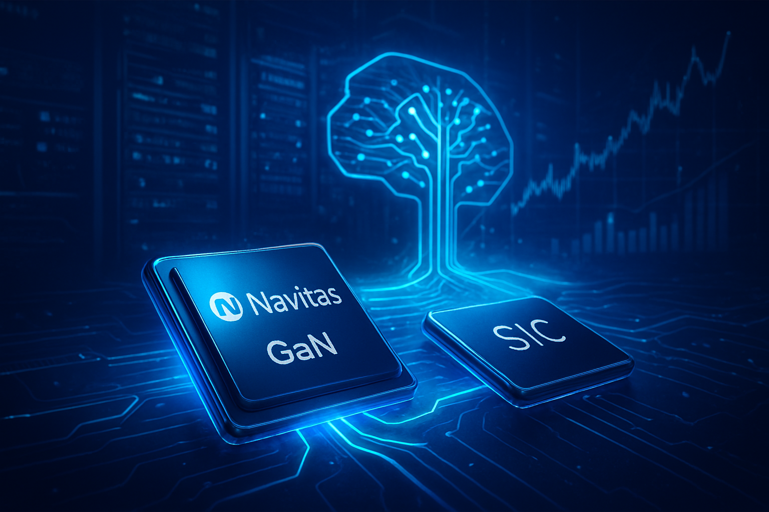
    This technical prowess and ecosystem dominance differentiate NVIDIA significantly from its rivals. While Advanced Micro Devices (AMD) (NASDAQ: AMD) offers its Instinct MI series GPUs (MI300X, upcoming MI350) and the open-source ROCm software platform, ROCm generally has less developer adoption and a less mature ecosystem compared to CUDA. AMD's MI300X has shown competitiveness in AI inference, particularly for LLMs, but often struggles against NVIDIA's H200 and lacks the broad software optimization of CUDA. Similarly, Intel (NASDAQ: INTC), with its Gaudi AI accelerators and Max Series GPUs unified by the oneAPI software stack, aims for cross-architecture portability but faces an uphill battle against NVIDIA's established dominance and developer mindshare. Furthermore, hyperscalers like Google (NASDAQ: GOOGL) with its TPUs, Amazon Web Services (AWS) (NASDAQ: AMZN) with Inferentia/Trainium, and Microsoft (NASDAQ: MSFT) with Maia 100, are developing custom AI chips to optimize for their specific workloads and reduce NVIDIA dependence, but these are primarily for internal cloud use and do not offer the broad general-purpose utility of NVIDIA's GPUs.

    Shifting Sands: Impact on the AI Ecosystem

    NVIDIA's pervasive influence profoundly impacts the entire AI ecosystem, from leading AI labs to burgeoning startups, creating a complex dynamic of reliance, competition, and strategic maneuvering.

    Leading AI companies like OpenAI, Anthropic, and xAI are direct beneficiaries, heavily relying on NVIDIA's powerful GPUs for training and deploying their advanced AI models at scale. NVIDIA strategically reinforces this "virtuous cycle" through investments in these startups, further embedding its technology. However, these companies also grapple with the high cost and scarcity of GPU clusters, exacerbated by NVIDIA's significant pricing power.

    Tech giants, particularly hyperscale cloud service providers such as Microsoft, Alphabet (Google's parent company), Amazon, and Meta (NASDAQ: META), represent NVIDIA's largest customers and, simultaneously, its most formidable long-term competitors. They pour billions into NVIDIA's data center GPUs, with these four giants alone accounting for over 40% of NVIDIA's revenue. Yet, to mitigate dependence and gain greater control over their AI infrastructure, they are aggressively developing their own custom AI chips. This "co-opetition" defines the current landscape, where NVIDIA is both an indispensable partner and a target for in-house disruption.

    Beyond the giants, numerous companies benefit from NVIDIA's expansive ecosystem. Memory manufacturers like Micron Technology (NASDAQ: MU) and SK Hynix see increased demand for High-Bandwidth Memory (HBM). Taiwan Semiconductor Manufacturing Company (TSMC) (NYSE: TSM), NVIDIA's primary foundry, experiences higher utilization of its advanced manufacturing processes. Specialized GPU-as-a-service providers like CoreWeave and Lambda thrive by offering access to NVIDIA's hardware, while data center infrastructure companies and networking providers like Broadcom (NASDAQ: AVGO) and Marvell Technology (NASDAQ: MRVL) also benefit from the AI buildout. NVIDIA's strategic advantages, including its unassailable CUDA ecosystem, its full-stack AI platform approach (from silicon to software, including DGX systems and NVIDIA AI Enterprise), and its relentless innovation, are expected to sustain its influence for the foreseeable future.

    Broader Implications and Historical Parallels

    NVIDIA's commanding position in late 2025 places it at the epicenter of broader AI landscape trends, yet also brings significant concerns regarding market concentration and supply chain vulnerabilities.

    The company's near-monopoly in AI chips (estimated 70-95% market share) has drawn antitrust scrutiny from regulatory bodies in the USA, EU, and China. The proprietary nature of CUDA creates a significant "lock-in" effect for developers and enterprises, potentially stifling the growth of alternative hardware and software solutions. This market concentration has spurred major cloud providers to invest heavily in their own custom AI chips, seeking to diversify their infrastructure and reduce reliance on a single vendor. Despite NVIDIA's strong fundamentals, some analysts voice concerns about an "AI bubble," citing rapid valuation increases and "circular funding deals" where NVIDIA invests in AI companies that then purchase its chips.

    Supply chain vulnerabilities remain a persistent challenge. NVIDIA has faced production delays for advanced products like the GB200 NVL72 due to design complexities and thermal management issues. Demand for Blackwell chips "vastly exceeds supply" well into 2026, indicating potential bottlenecks in manufacturing and packaging, particularly for TSMC's CoWoS technology. Geopolitical tensions and U.S. export restrictions on advanced AI chips to China continue to impact NVIDIA's growth strategy, forcing the development of reduced-compute versions for the Chinese market and leading to inventory write-downs. NVIDIA's aggressive product cadence, with new architectures every six months, also strains its supply chain and manufacturing partners.

    NVIDIA's current influence in AI draws compelling parallels to pivotal moments in technological history. Its invention of the GPU in 1999 and the subsequent launch of CUDA in 2006 were foundational for the rise of modern AI, much like Intel's dominance in CPUs during the PC era or Microsoft's role with Windows. GPUs, initially for gaming, proved perfectly suited for the parallel computations required by deep learning, enabling breakthroughs like AlexNet in 2012 that ignited the modern AI era. While some compare the current AI boom to past speculative bubbles, a key distinction is that NVIDIA is a deeply established, profitable company reinvesting heavily in physical infrastructure, suggesting a more tangible demand compared to some speculative ventures of the past.

    The Horizon: Future Developments and Lingering Challenges

    NVIDIA's future outlook is characterized by continued aggressive innovation and strategic expansion into new AI domains, though significant challenges loom.

    In the near term (late 2025), the company will focus on the sustained deployment of its Blackwell architecture, with half a trillion dollars in orders confirmed for Blackwell and Rubin chips through 2026. The H200 will remain a key offering as Blackwell ramps up, driving "AI factories" – data centers optimized to "manufacture intelligence at scale." The expansion of NVIDIA's software ecosystem, including NVIDIA Inference Microservices (NIM) and NeMo, will be critical for simplifying AI application development. Experts predict an increasing deployment of "AI agents" in enterprises, driving demand for NVIDIA's compute.

    Longer term (beyond 2025), NVIDIA's vision extends to "Physical AI," with robotics identified as "the next phase of AI." Through platforms like Omniverse and Isaac, NVIDIA is investing heavily in an AI-powered robot workforce, developing foundation models like Isaac GR00T N1 for humanoid robotics. The automotive industry remains a key focus, with DRIVE Thor expected to leverage Blackwell architecture for autonomous vehicles. NVIDIA is also exploring quantum computing integration, aiming to link quantum systems with classical supercomputers via NVQLink and CUDA-Q. Potential applications span data centers, robotics, autonomous vehicles, healthcare (e.g., Clara AI Platform for drug discovery), and various enterprise solutions for real-time analytics and generative AI.

    However, NVIDIA faces enduring challenges. Intense competition from AMD and Intel, coupled with the rising tide of custom AI chips from tech giants, could erode its market share in specific segments. Geopolitical risks, particularly export controls to China, remain a significant headwind. Concerns about market saturation in AI training and the long-term durability of demand persist, alongside the inherent supply chain vulnerabilities tied to its reliance on TSMC for advanced manufacturing. NVIDIA's high valuation also makes its stock susceptible to volatility based on market sentiment and earnings guidance.

    Experts predict NVIDIA will maintain its strong leadership through late 2025 and mid-2026, with the AI chip market projected to exceed $150 billion in 2025. They foresee a shift towards liquid cooling in AI data centers and the proliferation of AI agents. While NVIDIA's dominance in AI data center GPUs (estimated 92% market share in 2025) is expected to continue, some analysts anticipate custom AI chips and AMD's offerings to gain stronger traction in 2026 and beyond, particularly for inference workloads. NVIDIA's long-term success will hinge on its continued innovation, its expansion into software and "Physical AI," and its ability to navigate a complex competitive and geopolitical landscape.

    A Legacy Forged in Silicon: The AI Era's Defining Force

    In summary, NVIDIA's competitive landscape in late 2025 is one of unparalleled dominance, driven by its technological prowess in GPU architectures (Hopper, Blackwell, Rubin) and the unyielding power of its CUDA software ecosystem. This full-stack approach has cemented its role as the foundational infrastructure provider for the global AI revolution, enabling breakthroughs across industries and powering the largest AI models. Its financial performance reflects this, with record revenues and an aggressive product roadmap that promises continued innovation.

    NVIDIA's significance in AI history is profound, akin to the foundational impact of Intel in the PC era or Microsoft with operating systems. Its pioneering work in GPU-accelerated computing and the establishment of CUDA as the industry standard were instrumental in igniting the deep learning revolution. This legacy continues to shape the trajectory of AI development, making NVIDIA an indispensable force.

    Looking ahead, NVIDIA's long-term impact will be defined by its ability to push into new frontiers like "Physical AI" through robotics, further entrench its software ecosystem, and maintain its innovation cadence amidst intensifying competition. The challenges of supply chain vulnerabilities, geopolitical tensions, and the rise of custom silicon from hyperscalers will test its resilience. What to watch in the coming weeks and months includes the successful rollout and demand for the Blackwell Ultra chips, NVIDIA's Q4 FY2026 earnings and guidance, the performance and market adoption of competitor offerings from AMD and Intel, and the ongoing efforts of hyperscalers to deploy their custom AI accelerators. Any shifts in TSMC's CoWoS capacity or HBM supply will also be critical indicators of future market dynamics and NVIDIA's pricing power.


    This content is intended for informational purposes only and represents analysis of current AI developments.

    TokenRing AI delivers enterprise-grade solutions for multi-agent AI workflow orchestration, AI-powered development tools, and seamless remote collaboration platforms.
    For more information, visit https://www.tokenring.ai/.

  • India’s Semiconductor Ambition Ignites: Private Investment Fuels Drive for Global Tech Hub Status

    India’s Semiconductor Ambition Ignites: Private Investment Fuels Drive for Global Tech Hub Status

    India is rapidly accelerating its strategic push to establish a robust domestic semiconductor industry, a move poised to fundamentally reshape its economic landscape and solidify its position as a global technology powerhouse. Driven by a proactive government framework and an unprecedented surge in private investment, the nation is transitioning from a consumer of chips to a significant producer, aiming for technological self-reliance and substantial economic growth. This concerted effort marks a pivotal moment, signaling India's intent to become a critical node in the global semiconductor supply chain and a major hub for innovation and electronics manufacturing in the immediate future.

    The immediate significance of this development is profound. India's semiconductor strategy has swiftly transitioned from policy blueprints to active implementation, with three Indian chip facilities anticipated to begin commercial production as early as 2026. This rapid shift to execution, validated by increasing private capital flow alongside government incentives, underscores the effectiveness of India's policy framework in creating a conducive environment for semiconductor manufacturing. It lays a stable foundation for sustained, long-term private sector involvement, addressing the nation's surging domestic demand for chips across critical sectors like mobile devices, IT, automotive, 5G infrastructure, and artificial intelligence, thereby reducing import dependency and fostering a vertically integrated ecosystem.

    India's Chip Blueprint: From Policy to Production

    India's strategic framework to cultivate its domestic semiconductor industry is meticulously designed and spearheaded by the India Semiconductor Mission (ISM), launched in December 2021 with a substantial financial commitment of approximately $10 billion (₹76,000 crore). Operating under the Ministry of Electronics and Information Technology (MeitY), the ISM acts as the nodal agency for investment screening and scheme implementation across the entire semiconductor value chain.

    The core of this strategy involves comprehensive fiscal support, offering significant financial incentives, including up to 50% of the project cost for setting up semiconductor fabrication plants (fabs) and 50% of the capital expenditure for compound semiconductor fabs, silicon photonics, sensors, and Assembly, Testing, Marking, and Packaging (ATMP)/Outsourced Semiconductor Assembly and Test (OSAT) facilities. Notably, recent modifications ensure a 50% subsidy for all node sizes, reflecting a pragmatic approach to initially focus on trailing-edge nodes before progressing towards leading-edge technologies. This flexibility is a key differentiator from earlier, less successful attempts, which often aimed for leading-edge technology without sufficient foundational support.

    Further bolstering this push is the Design Linked Incentive (DLI) Scheme, a vital component of the ISM aimed at fostering a full-stack chip design ecosystem. It provides financial support to semiconductor startups and Micro, Small, and Medium Enterprises (MSMEs) to recover design costs, scale commercialization, and develop intellectual property. As of July 2025, 23 chip design projects have been approved, and 72 companies have gained access to industry-grade Electronic Design Automation (EDA) tools, demonstrating tangible progress. This focus on design, where India already contributes 30% to global chip design, leverages an existing strength to accelerate its position in high-value segments. Initial reactions from the AI research community and industry experts have been largely positive, viewing India's holistic approach – encompassing design, fabrication, and packaging – as a more sustainable and robust strategy compared to fragmented efforts in the past. The commitment to indigenous innovation, exemplified by the expected unveiling of India's first indigenous semiconductor chip, Vikram-32, by late 2025, further reinforces confidence in the nation's long-term vision.

    Corporate Catalysts: How Giants and Startups Are Shaping India's Chip Future

    The burgeoning semiconductor landscape in India is attracting significant investment from both global tech giants and ambitious domestic players, poised to reshape competitive dynamics and create new market opportunities. This influx of capital and expertise signals a powerful endorsement of India's strategic vision and its potential to emerge as a formidable force in the global chip industry.

    Among the most prominent beneficiaries and drivers of this development are companies like Micron Technology (NASDAQ: MU), which in June 2023, announced a substantial investment of approximately $2.71 billion (₹22,516 crore) to establish an advanced Assembly, Testing, Marking, and Packaging (ATMP) facility in Sanand, Gujarat. This facility, already under setup, represents a critical step in building out India's manufacturing capabilities. Similarly, the Tata Group, through Tata Electronics Private Limited, has committed a staggering $10 billion investment in a semiconductor fab, alongside Tata Semiconductor Assembly and Test (TSAT) setting up a $3.3 billion ATMP unit in Morigaon, Assam. These massive investments from established industrial conglomerates underscore the scale of ambition and the confidence in India's long-term semiconductor prospects.

    The competitive implications for major AI labs and tech companies are significant. As India develops its indigenous manufacturing capabilities, it offers a diversified and potentially more resilient supply chain alternative to existing hubs. This could reduce reliance on single regions, a critical factor given recent geopolitical tensions and supply chain disruptions. Companies that partner with or establish operations in India stand to benefit from government incentives, a vast talent pool, and access to a rapidly growing domestic market. The focus on the entire value chain, from design to packaging, also creates opportunities for specialized equipment manufacturers like Applied Materials (NASDAQ: AMAT), which is investing $400 million in an engineering center, and Lam Research (NASDAQ: LRCX), pledging $25 million for a semiconductor training lab. This comprehensive approach ensures that the ecosystem is supported by critical infrastructure and talent development.

    Furthermore, the Design Linked Incentive (DLI) scheme is fostering a vibrant startup ecosystem. Indian semiconductor startups have already garnered $43.9 million in private investment, with companies like Netrasemi, Mindgrove Technologies (developing India's first commercial-grade high-performance microcontroller SoC), and Fermionic Design innovating in areas such as AI, IoT, and satellite communication chips. This surge in homegrown innovation not only creates new market entrants but also positions India as a hub for cutting-edge IP development, potentially disrupting existing product lines and services that rely solely on imported chip designs. The strategic advantages gained by these early movers, both large corporations and nimble startups, will be crucial in shaping their market positioning in the evolving global technology landscape.

    India's Chip Ambition: Reshaping the Global Tech Tapestry

    India's aggressive push into the semiconductor industry is more than just an economic initiative; it's a strategic move that significantly alters the broader AI landscape and global technology trends. By aiming for self-reliance in chip manufacturing, India is addressing a critical vulnerability exposed by recent global supply chain disruptions and geopolitical shifts, positioning itself as a vital alternative in a concentrated market.

    This fits into the broader AI landscape by securing the foundational hardware necessary for advanced AI development and deployment. AI models and applications are inherently compute-intensive, requiring a constant supply of high-performance chips. By building domestic fabrication capabilities, India ensures a stable and secure supply for its rapidly expanding AI sector, from data centers to edge devices. The indigenous development of chips, such as the upcoming Vikram-32, will not only cater to domestic demand but also foster innovation tailored to India's unique market needs and technological aspirations, including applications in smart cities, healthcare, and defense. This move also contributes to the global trend of decentralizing semiconductor manufacturing, moving away from a few dominant regions to a more distributed and resilient model.

    The impacts are multi-faceted. Economically, India's semiconductor market, valued at approximately $38 billion in 2023, is projected to surge to $100-110 billion by 2030, demonstrating a compound annual growth rate (CAGR) of 13.8%. This growth is expected to generate 1 million jobs by 2026, boosting employment and skill development across various technical domains. Geopolitically, India's emergence as a reliable alternative in the global semiconductor supply chain enhances its strategic importance and contributes to global stability by diversifying critical technology sources. However, potential concerns include the immense capital expenditure required, the complexity of establishing a mature ecosystem, and the challenge of attracting and retaining highly specialized talent. Comparisons to previous AI milestones and breakthroughs highlight that while AI software advancements often grab headlines, the underlying hardware infrastructure, like semiconductors, is equally critical. India's strategy acknowledges this foundational truth, ensuring that its AI ambitions are supported by robust, domestically controlled hardware.

    The Road Ahead: India's Semiconductor Horizon

    The future trajectory of India's semiconductor industry is marked by ambitious targets and significant expected developments, poised to further solidify its standing on the global stage. Near-term, the focus remains on operationalizing the approved projects and bringing the first set of facilities into commercial production. The anticipated commencement of production from three Indian chip facilities as early as 2026 will be a critical milestone, demonstrating tangible progress from policy to product.

    In the long term, experts predict that India will continue its strategic progression from trailing-edge to more advanced node technologies, driven by sustained private investment and continuous government support. The goal, as articulated by Union Minister Ashwini Vaishnaw, is for India to achieve semiconductor manufacturing capabilities on par with leading global chipmaking nations like the US and China by 2031-2032. This will involve not just manufacturing but also significant advancements in research and development, fostering indigenous intellectual property, and expanding the design ecosystem. Potential applications and use cases on the horizon are vast, ranging from powering India's burgeoning AI and IoT sectors, enabling advanced 5G and future 6G communication infrastructure, to enhancing automotive electronics and defense technologies. The development of specialized chips for AI accelerators and edge computing will be particularly crucial as AI integration deepens across industries.

    However, several challenges need to be addressed. Securing access to advanced technology licenses, establishing a robust supply chain for critical raw materials and equipment, and continuously upskilling a vast workforce to meet the highly specialized demands of semiconductor manufacturing are paramount. Furthermore, maintaining a competitive incentive structure and ensuring policy stability will be crucial to attract and retain global players. Experts predict that while the initial phase will focus on establishing foundational capabilities, subsequent phases will see India making significant inroads into more complex fabrication processes and specialized chip designs, driven by a growing pool of engineering talent and increasing global collaborations. The continuous evolution of the Design Linked Incentive (DLI) scheme and the active participation of state governments will be key enablers for this growth.

    India's Chip Renaissance: A New Era for Global Tech

    India's strategic pivot to cultivate a robust domestic semiconductor industry represents a monumental shift with far-reaching implications for the global technology landscape. The key takeaways underscore a nation that has moved beyond aspirations to concrete execution, evidenced by substantial government backing through the India Semiconductor Mission and an unprecedented surge in private investment from both international giants and homegrown conglomerates. This combined force is rapidly laying the groundwork for a comprehensive semiconductor ecosystem, spanning design, fabrication, and packaging.

    The significance of this development in AI history cannot be overstated. As AI continues its exponential growth, the demand for sophisticated, high-performance chips will only intensify. By building its own chip manufacturing capabilities, India is not merely diversifying its economy; it is securing the foundational hardware necessary to power its AI ambitions and contribute to the global AI revolution. This self-reliance ensures resilience against future supply chain shocks and positions India as a strategic partner in the development of cutting-edge AI technologies. The long-term impact will see India emerge not just as a consumer, but as a critical producer and innovator in the global semiconductor and AI arenas, fostering indigenous IP and creating a vast pool of highly skilled talent.

    In the coming weeks and months, the world will be watching for several key indicators: the progress of the Micron and Tata facilities towards commercial production, further announcements of private investments, and the unveiling of indigenous chip designs. The success of the DLI scheme in nurturing startups and the continued evolution of state-level policies will also be crucial barometers of India's sustained momentum. India's chip renaissance is not just an economic story; it's a testament to national ambition, technological foresight, and a determined push to redefine its role in shaping the future of global technology.


    This content is intended for informational purposes only and represents analysis of current AI developments.

    TokenRing AI delivers enterprise-grade solutions for multi-agent AI workflow orchestration, AI-powered development tools, and seamless remote collaboration platforms.
    For more information, visit https://www.tokenring.ai/.

  • TSMC Rocked by Alleged 2nm and A16 Secret Leak: Former Executive Under Scrutiny

    Hsinchu, Taiwan – November 20, 2025 – Taiwan Semiconductor Manufacturing Company (TSMC) (NYSE: TSM), the world's leading contract chipmaker, finds itself embroiled in a high-stakes investigation following the suspected leak of its most advanced manufacturing secrets. The alleged breach centers on highly coveted 2-nanometer (2nm), A16, and A14 process technologies, critical for the next generation of high-performance computing and artificial intelligence. This incident has sent ripples through the global semiconductor industry, raising urgent questions about intellectual property protection and the intense competition for technological supremacy.

    The allegations primarily target Lo Wei-jen, a former Senior Vice President for Corporate Strategy Development at TSMC, who retired in July 2025 after a distinguished 21-year career with the company. Prosecutors officially launched an investigation on November 19, 2025, into claims that Lo Wei-jen may have taken confidential documents related to these cutting-edge processes, potentially transferring them to Intel (NASDAQ: INTC), a company he reportedly joined in late October 2025. This development comes on the heels of earlier internal suspicions at TSMC and a broader crackdown on industrial espionage in Taiwan's critical semiconductor sector.

    Unpacking the Alleged Breach: The Crown Jewels of Chipmaking at Risk

    The core of the alleged leak involves TSMC's 2nm, A16, and A14 process technologies, representing the pinnacle of semiconductor manufacturing. The 2nm process, in particular, is a game-changer, promising unprecedented transistor density, power efficiency, and performance gains crucial for powering advanced AI accelerators, high-end mobile processors, and data center infrastructure. These technologies are not merely incremental improvements; they are foundational advancements that dictate the future trajectory of computing power and innovation across industries.

    While specific technical specifications of the allegedly leaked information remain under wraps due to the ongoing investigation, the sheer significance of 2nm technology lies in its ability to pack more transistors into a smaller area, enabling more complex and powerful chips with reduced energy consumption. This leap in miniaturization is achieved through novel transistor architectures and advanced lithography techniques, differentiating it significantly from existing 3nm or 4nm processes currently in mass production. The A16 and A14 processes further extend this technological lead, indicating TSMC's roadmap for continued dominance. Initial reactions from the AI research community and industry experts, though cautious due to the lack of confirmed details, underscore the potential competitive advantage such information could confer. The consensus is that any insight into these proprietary processes could shave years off development cycles for competitors, particularly in the race to develop more powerful and efficient AI hardware.

    This incident differs markedly from typical employee departures, where knowledge transfer is often limited to general strategic insights. The allegations suggest a systematic attempt to extract detailed technical documentation, reportedly involving requests for comprehensive briefings on advanced technologies prior to retirement and the physical removal of a significant volume of data. This level of alleged misconduct points to a calculated effort to compromise TSMC's technological lead, rather than an incidental transfer of general expertise.

    Competitive Whirlwind: Reshaping the Semiconductor Landscape

    The potential leak of TSMC's 2nm, A16, and A14 process technologies carries profound implications for AI companies, tech giants, and startups alike. If the allegations prove true, Intel (NASDAQ: INTC), the company Lo Wei-jen allegedly joined, stands to potentially benefit from this development. Access to TSMC's advanced process know-how could significantly accelerate Intel's efforts to catch up in the foundry space and bolster its own manufacturing capabilities, particularly as it aims to reclaim its leadership in chip technology and become a major contract chipmaker. This could directly impact its ability to produce competitive AI chips and high-performance CPUs.

    The competitive implications for major AI labs and tech companies are immense. Companies like NVIDIA (NASDAQ: NVDA), Apple (NASDAQ: AAPL), and Qualcomm (QCOM), which rely heavily on TSMC's cutting-edge manufacturing for their AI accelerators and mobile processors, could face a more diversified and potentially more competitive foundry landscape in the long run. While TSMC's immediate market position as the dominant advanced foundry remains strong, any erosion of its unique technological advantage could lead to increased pressure on pricing and lead times. For startups in the AI hardware space, a more competitive foundry market could offer more options, but also introduces uncertainty regarding the future availability and pricing of the most advanced nodes.

    Potential disruption to existing products or services could manifest if competitors leverage the leaked information to rapidly close the technology gap, forcing TSMC's customers to reassess their supply chain strategies. This scenario could lead to a reshuffling of orders and a more fragmented market for advanced chip manufacturing. TSMC's strategic advantage has long been its unparalleled process technology leadership. A successful breach of these core secrets could undermine that advantage, impacting its market positioning and potentially altering the competitive dynamics between pure-play foundries and integrated device manufacturers (IDMs).

    Broader Ramifications: A Wake-Up Call for IP Protection

    This alleged leak fits into a broader, escalating trend of industrial espionage and intellectual property theft within the global technology sector, particularly concerning critical national technologies like semiconductors. Taiwan, a global leader in chip manufacturing, has been increasingly vigilant against such threats, especially given the geopolitical significance of its semiconductor industry. The incident underscores the immense value placed on advanced chipmaking know-how and the lengths to which competitors or state-backed actors might go to acquire it.

    The impacts extend beyond mere corporate competition. Such leaks raise significant concerns about supply chain security and national economic resilience. If core technologies of a critical industry leader like TSMC can be compromised, it could have cascading effects on global technology supply chains, impacting everything from consumer electronics to defense systems. This incident also draws comparisons to previous AI milestones and breakthroughs where proprietary algorithms or architectural designs were fiercely protected, highlighting that the battle for technological supremacy is fought not just in research labs but also in the realm of corporate espionage.

    Potential concerns include the long-term erosion of trust within the industry, increased costs for security measures, and a more protectionist stance from technology-leading nations. The incident serves as a stark reminder that as AI and other advanced technologies become more central to economic and national security, the safeguarding of the underlying intellectual property becomes paramount.

    The Road Ahead: Navigating Uncertainty and Bolstering Defenses

    In the near-term, the focus will be on the ongoing investigation by Taiwanese prosecutors. The outcome of this probe, including any indictments and potential legal ramifications for Lo Wei-jen and others involved, will be closely watched. TSMC is expected to double down on its internal security protocols and intellectual property protection measures, potentially implementing even stricter access controls, monitoring systems, and employee agreements. The company's "zero-tolerance policy" for IP violations will likely be reinforced with more robust enforcement mechanisms.

    Long-term developments could see a re-evaluation of industry practices regarding employee mobility, particularly for senior executives with access to highly sensitive information. There might be increased calls for stricter non-compete clauses and extended cooling-off periods for individuals transitioning between rival companies, especially across national borders. Potential applications and use cases on the horizon for TSMC include further advancements in 2nm and beyond, catering to the ever-increasing demands of AI and high-performance computing. However, challenges that need to be addressed include maintaining talent while preventing knowledge transfer, balancing innovation with security, and navigating a complex geopolitical landscape where technological leadership is a strategic asset.

    Experts predict that this incident will serve as a significant catalyst for the entire semiconductor industry to review and strengthen its IP protection strategies. It's also likely to intensify the global competition for top engineering talent, as companies seek to innovate internally while simultaneously safeguarding their existing technological advantages.

    A Critical Juncture for Semiconductor Security

    The suspected leak of TSMC's core technical secrets marks a critical juncture in the ongoing battle for technological supremacy in the semiconductor industry. The allegations against former executive Lo Wei-jen, involving the company's most advanced 2nm, A16, and A14 process technologies, underscore the immense value of intellectual property in today's high-tech landscape. The incident highlights not only the internal vulnerabilities faced by even the most secure companies but also the broader implications for national security and global supply chains.

    The significance of this development in AI history cannot be overstated. As AI applications become more sophisticated, they demand increasingly powerful and efficient underlying hardware. Any compromise of the foundational manufacturing processes that enable such hardware could have far-reaching consequences, potentially altering competitive dynamics, delaying technological progress, and impacting the availability of cutting-edge AI solutions.

    What to watch for in the coming weeks and months includes the progress of the judicial investigation, any official statements from TSMC or Intel, and the industry's response in terms of tightening security measures. This event serves as a potent reminder that in the race for AI dominance, the protection of intellectual property is as crucial as the innovation itself.


    This content is intended for informational purposes only and represents analysis of current AI developments.

    TokenRing AI delivers enterprise-grade solutions for multi-agent AI workflow orchestration, AI-powered development tools, and seamless remote collaboration platforms.
    For more information, visit https://www.tokenring.ai/.

  • Nvidia’s AI Reign Intensifies: Record Earnings Ignite Global Semiconductor and AI Markets

    Nvidia’s AI Reign Intensifies: Record Earnings Ignite Global Semiconductor and AI Markets

    San Francisco, CA – November 20, 2025 – Nvidia Corporation (NASDAQ: NVDA) sent seismic waves through the global technology landscape yesterday, November 19, 2025, with the release of its Q3 Fiscal Year 2026 earnings report. The semiconductor giant not only shattered analyst expectations but also provided an exceptionally bullish outlook, reinforcing its indispensable role in the accelerating artificial intelligence revolution. This landmark report has reignited investor confidence, propelling Nvidia's stock and triggering a significant rally across the broader semiconductor and AI markets worldwide.

    The stellar financial performance, overwhelmingly driven by an insatiable demand for Nvidia's cutting-edge AI chips and data center solutions, immediately dispelled lingering concerns about a potential "AI bubble." Instead, it validated the massive capital expenditures by tech giants and underscored the sustained, exponential growth trajectory of the AI sector. Nvidia's results are a clear signal that the world is in the midst of a fundamental shift towards AI-centric computing, with the company firmly positioned as the primary architect of this new era.

    Blackwell Architecture Fuels Unprecedented Data Center Dominance

    Nvidia's Q3 FY2026 earnings report painted a picture of extraordinary growth, with the company reporting a record-breaking revenue of $57 billion, a staggering 62% increase year-over-year and a 22% rise from the previous quarter. This significantly surpassed the anticipated $54.89 billion to $55.4 billion. Diluted earnings per share (EPS) also outperformed, reaching $1.30 against an expected $1.25 or $1.26, while net income surged by 65% to $31.9 billion. The overwhelming driver of this success was Nvidia's Data Center segment, which alone generated a record $51.2 billion in revenue, marking a 66% year-over-year increase and a 25% sequential jump, now accounting for approximately 90% of the company's total revenue.

    At the heart of this data center explosion lies Nvidia's revolutionary Blackwell architecture. Chips like the GB200 and B200 represent a monumental leap over the previous Hopper generation (H100, H200), designed explicitly for the demands of massive Generative AI and agentic AI workloads. Built on TSMC's (NYSE: TSM) custom 4NP process, Blackwell GPUs feature a staggering 208 billion transistors—2.5 times more than Hopper's 80 billion. The B200 GPU, for instance, utilizes a unified dual-die design linked by an ultra-fast 10 TB/s chip-to-chip interconnect, allowing it to function as a single, powerful CUDA GPU. Blackwell also introduces NVFP4 precision, a new 4-bit floating-point format that can double inference performance while reducing memory consumption compared to Hopper's FP8, delivering up to 20 petaflops of AI performance (FP4) from a single B200 GPU.

    Further enhancing its capabilities, Blackwell incorporates a second-generation Transformer Engine optimized for FP8 and the new FP4 precision, crucial for accelerating transformer model training and inference. With up to 192 GB of HBM3e memory and approximately 8 TB/s of bandwidth, alongside fifth-generation NVLink offering 1.8 TB/s of bidirectional bandwidth per GPU, Blackwell provides unparalleled data processing power. Nvidia CEO Jensen Huang emphatically stated that "Blackwell sales are off the charts, and cloud GPUs are sold out," underscoring the insatiable demand. He further elaborated that "Compute demand keeps accelerating and compounding across training and inference — each growing exponentially," indicating that the company has "entered the virtuous cycle of AI." This sold-out status and accelerating demand validate the continuous and massive investment in AI infrastructure by hyperscalers and cloud providers, providing strong long-term revenue visibility, with Nvidia already securing over $500 billion in cumulative orders for its Blackwell and Rubin chips through the end of calendar 2026.

    Industry experts have reacted with overwhelming optimism, viewing Nvidia's performance as a strong validation of the AI sector's "explosive growth potential" and a direct rebuttal to the "AI bubble" narrative. Analysts emphasize Nvidia's structural advantages, including its robust ecosystem of partnerships and dominant market position, which makes it a "linchpin" in the AI sector. Despite the bullish sentiment, some caution remains regarding geopolitical risks, such as U.S.-China export restrictions, and rising competition from hyperscalers developing custom AI accelerators. However, the sheer scale of Blackwell's technical advancements and market penetration has solidified Nvidia's position as the leading enabler of the AI revolution.

    Reshaping the AI Landscape: Beneficiaries, Competitors, and Disruption

    Nvidia's strong Q3 FY2026 earnings, fueled by the unprecedented demand for Blackwell AI chips and data center growth, are profoundly reshaping the competitive landscape across AI companies, tech giants, and startups. The ripple effect of this success is creating direct and indirect beneficiaries while intensifying competitive pressures and driving significant market disruptions.

    Direct Beneficiaries: Nvidia Corporation (NASDAQ: NVDA) itself stands as the primary beneficiary, solidifying its near-monopoly in AI chips and infrastructure. Major hyperscalers and cloud service providers (CSPs) like Microsoft (NASDAQ: MSFT) (Azure), Amazon (NASDAQ: AMZN) (AWS), Google (NASDAQ: GOOGL) (Google Cloud), and Meta Platforms (NASDAQ: META), along with Oracle Corporation (NYSE: ORCL), are massive purchasers of Blackwell chips, investing billions to expand their AI infrastructure. Key AI labs and foundation model developers such as OpenAI, Anthropic, and xAI are deploying Nvidia's platforms to train their next-generation AI models. Furthermore, semiconductor manufacturing and supply chain companies, most notably Taiwan Semiconductor Manufacturing Company (NYSE: TSM), and high-bandwidth memory (HBM) suppliers like Micron Technology (NASDAQ: MU), are experiencing a surge in demand. Data center infrastructure providers, including Super Micro Computer (NASDAQ: SMCI), also benefit significantly.

    Competitive Implications: Nvidia's performance reinforces its near-monopoly in the AI chip market, particularly for AI training workloads. Blackwell's superior performance (up to 30 times faster for AI inference than its predecessors) and energy efficiency set a new benchmark, making it exceedingly challenging for competitors to catch up. The company's robust CUDA software ecosystem creates a powerful "moat," making it difficult and costly for developers to switch to alternative hardware. While Advanced Micro Devices (NASDAQ: AMD) with its Instinct GPUs and Intel Corporation (NASDAQ: INTC) with its Gaudi chips are making strides, they face significant disparities in market presence and technological capabilities. Hyperscalers' custom chips (e.g., Google TPUs, AWS Trainium) are gaining market share in the inference segment, but Nvidia continues to dominate the high-margin training market, holding over 90% market share for AI training accelerator deployments. Some competitors, like AMD and Intel, are even supporting Nvidia's MGX architecture, acknowledging the platform's ubiquity.

    Potential Disruption: The widespread adoption of Blackwell chips and the surge in data center demand are driving several key disruptions. The immense computing power enables the training of vastly larger and more complex AI models, accelerating progress in fields like natural language processing, computer vision, and scientific simulation, leading to more sophisticated AI products and services across all sectors. Nvidia CEO Jensen Huang notes a fundamental global shift from traditional CPU-reliant computing to AI-infused systems heavily dependent on GPUs, meaning existing software and hardware not optimized for AI acceleration may become less competitive. This also facilitates the development of more autonomous and capable AI agents, potentially disrupting various industries by automating complex tasks and improving decision-making.

    Nvidia's Q3 FY2026 performance solidifies its market positioning as the "engine" of the AI revolution and an "essential infrastructure provider" for the next computing era. Its consistent investment in R&D, powerful ecosystem lock-in through CUDA, and strategic partnerships with major tech giants ensure continued demand and integration of its technology, while robust supply chain management allows it to maintain strong gross margins and pricing power. This validates the massive capital expenditures by tech giants and reinforces the long-term growth trajectory of the AI market.

    The AI Revolution's Unstoppable Momentum: Broader Implications and Concerns

    Nvidia's phenomenal Q3 FY2026 earnings and the unprecedented demand for its Blackwell AI chips are not merely financial triumphs; they are a resounding affirmation of AI's transformative power, signaling profound technological, economic, and societal shifts. This development firmly places AI at the core of global innovation, while also bringing to light critical challenges that warrant careful consideration.

    The "off the charts" demand for Blackwell chips and Nvidia's optimistic Q4 FY2026 guidance of $65 billion underscore a "virtuous cycle of AI," where accelerating compute demand across training and inference is driving exponential growth across industries and countries. Nvidia's Blackwell platform is rapidly becoming the leading architecture for all customer categories, from cloud hyperscalers to sovereign AI initiatives, pushing a new wave of performance and efficiency upgrades. This sustained momentum validates the immense capital expenditure flowing into AI infrastructure, with Nvidia's CEO Jensen Huang suggesting that total revenue for its Blackwell and upcoming Rubin platforms could exceed the previously announced $500 billion target through 2026.

    Overall Impacts: Technologically, Blackwell's superior processing speed and reduced power consumption per watt are enabling the creation of more complex AI models and applications, fostering breakthroughs in medicine, scientific research, and advanced robotics. Economically, the AI boom, heavily influenced by Nvidia, is projected to be a significant engine of productivity and global GDP growth, with Goldman Sachs predicting a 7% annual boost over a decade. However, this transformation also carries disruptive effects, including potential job displacement in repetitive tasks and market polarization, necessitating significant workforce retraining. Societally, AI promises advancements in healthcare and education, but also raises concerns about misinformation, blanket surveillance, and critical ethical considerations around bias, privacy, transparency, and accountability.

    Potential Concerns: Nvidia's near-monopoly in the AI chip market, particularly for large-scale AI model training, raises significant concerns about market concentration. While this dominance fuels its growth, it also poses questions about competition and the potential for a few companies to control the core infrastructure of the AI revolution. Another pressing issue is the immense energy consumption of AI models. Training these models with thousands of GPUs running continuously for months leads to high electricity consumption, with data centers potentially reaching 20% of global electricity use by 2030–2035, straining power grids and demanding advanced cooling solutions. While newer chips like Blackwell offer increased performance per watt, the sheer scale of AI deployment requires substantial energy infrastructure investment and sustainable practices.

    Comparison to Previous AI Milestones: The current AI boom, driven by advancements like large language models and highly capable GPUs such as Blackwell, represents a seismic shift comparable to, and in some aspects exceeding, previous technological revolutions. Unlike earlier AI eras limited by computational power, or the deep learning era of the 2010s focused on specific tasks, the modern AI boom (2020s-present) is characterized by unparalleled breadth of application and pervasive integration into daily life. This era, powered by chips like Blackwell, differs in its potential for accelerated scientific progress, profound economic restructuring affecting both manual and cognitive tasks, and complex ethical and societal dilemmas that necessitate a fundamental re-evaluation of work and human-AI interaction. Nvidia's latest earnings are not just a financial success; they are a clear signal of AI's accelerating, transformative power, solidifying its role as a general-purpose technology set to reshape our world on an unprecedented scale.

    The Horizon of AI: From Agentic Systems to Sustainable Supercomputing

    Nvidia's robust Q3 FY2026 earnings and the sustained demand for its Blackwell AI chips are not merely a reflection of current market strength but a powerful harbinger of future developments across the AI and semiconductor industries. This momentum is driving an aggressive roadmap for hardware and software innovation, expanding the horizon of potential applications, and necessitating proactive solutions to emerging challenges.

    In the near term, Nvidia is maintaining an aggressive one-year cadence for new GPU architectures. Following the Blackwell architecture, which is currently shipping, the company plans to introduce the Blackwell Ultra GPU in the second half of 2025, promising about 1.5 times faster performance. Looking further ahead, the Rubin family of GPUs is slated for release in the second half of 2026, with an Ultra version expected in 2027, potentially delivering up to 30 times faster AI inferencing performance than their Blackwell predecessors. These next-generation chips aim for massive model scaling and significant reductions in cost and energy consumption, emphasizing multi-die architectures, advanced GPU pairing for seamless memory sharing, and a unified "One Architecture" approach to support model training and deployment across diverse hardware and software environments. Beyond general-purpose GPUs, the industry will see a continued proliferation of specialized AI chips, including Neural Processing Units (NPUs) and custom Application-Specific Integrated Circuits (ASICs) developed by cloud providers, alongside significant innovations in high-speed interconnects and 3D packaging.

    These hardware advancements are paving the way for a new generation of transformative AI applications. Nvidia CEO Jensen Huang has introduced the concept of "agentic AI," focusing on new reasoning models optimized for longer thought processes to deliver more accurate, context-aware responses across multiple modalities. This shift towards AI that "thinks faster" and understands context will broaden AI's applicability, leading to highly sophisticated generative AI applications across content creation, customer operations, software engineering, and scientific R&D. Enhanced data centers and cloud computing, driven by the integration of Nvidia's Grace Blackwell Superchips, will democratize access to advanced AI tools. Significant advancements are also expected in autonomous systems and robotics, with Nvidia making open-sourced foundational models available to accelerate robot development. Furthermore, AI adoption is driving substantial growth in AI-enabled PCs and smartphones, which are expected to become the standard for large businesses by 2026, incorporating more NPUs, GPUs, and advanced connectivity for AI-driven features.

    However, this rapid expansion faces several critical challenges. Supply chain disruptions, high production costs for advanced fabs, and the immense energy consumption and heat dissipation of AI workloads remain persistent hurdles. Geopolitical risks, talent shortages in AI hardware design, and data scarcity for model training also pose significant challenges. Experts predict a sustained market growth, with the global semiconductor industry revenue projected to reach $800 billion in 2025 and AI chips achieving sales of $400 billion by 2027. AI is becoming the primary driver for semiconductors, shifting capital expenditure from consumer markets to AI data centers. The future will likely see a balance of supply and demand for advanced chips by 2025 or 2026, a proliferation of domain-specific accelerators, and a shift towards hybrid AI architectures combining GPUs, CPUs, and ASICs. Growing concerns about environmental impact are also driving an increased focus on sustainability, with the industry exploring novel materials and energy solutions. Jensen Huang's prediction that all companies will operate two types of factories—one for manufacturing and one for mathematics—encapsulates the profound economic paradigm shift being driven by AI.

    The Dawn of a New Computing Era: A Comprehensive Wrap-Up

    Nvidia's Q3 Fiscal Year 2026 earnings report, delivered yesterday, November 19, 2025, stands as a pivotal moment, not just for the company but for the entire technology landscape. The record-breaking revenue of $57 billion, overwhelmingly fueled by the insatiable demand for its Blackwell AI chips and data center solutions, has cemented Nvidia's position as the undisputed architect of the artificial intelligence revolution. This report has effectively silenced "AI bubble" skeptics, validating the unprecedented capital investment in AI infrastructure and igniting a global rally across semiconductor and AI stocks.

    The key takeaway is clear: Nvidia is operating in a "virtuous cycle of AI," where accelerating compute demand across both training and inference is driving exponential growth. The Blackwell architecture, with its superior performance, energy efficiency, and advanced interconnects, is the indispensable engine powering the next generation of AI models and applications. Nvidia's strategic partnerships with hyperscalers, AI labs like OpenAI, and sovereign AI initiatives ensure its technology is at the core of the global AI build-out. The market's overwhelmingly positive reaction underscores strong investor confidence in the long-term sustainability and transformative power of AI.

    In the annals of AI history, this development marks a new era. Unlike previous milestones, the current AI boom, powered by Nvidia's relentless innovation, is characterized by its pervasive integration across all sectors, its potential to accelerate scientific discovery at an unprecedented rate, and its profound economic and societal restructuring. The long-term impact on the tech industry will be a complete reorientation towards AI-centric computing, driving continuous innovation in hardware, software, and specialized accelerators. For society, it promises advancements in every facet of life, from healthcare to autonomous systems, while simultaneously presenting critical challenges regarding market concentration, energy consumption, and ethical AI deployment.

    In the coming weeks and months, all eyes will remain on Nvidia's ability to maintain its aggressive growth trajectory and meet its ambitious Q4 FY2026 guidance. Monitoring the production ramp and sales figures for the Blackwell and upcoming Rubin platforms will be crucial indicators of sustained demand. The evolving competitive landscape, particularly the advancements from rival chipmakers and in-house efforts by tech giants, will shape the future market dynamics. Furthermore, the industry's response to the escalating energy demands of AI and its commitment to sustainable practices will be paramount. Nvidia's Q3 FY2026 report is not just a financial success; it is a powerful affirmation that we are at the dawn of a new computing era, with AI at its core, poised to reshape our world in ways we are only just beginning to comprehend.


    This content is intended for informational purposes only and represents analysis of current AI developments.

    TokenRing AI delivers enterprise-grade solutions for multi-agent AI workflow orchestration, AI-powered development tools, and seamless remote collaboration platforms.
    For more information, visit https://www.tokenring.ai/.

  • Semiconductor Insiders Cash Out: A Signal of Caution Amidst AI Hype?

    Semiconductor Insiders Cash Out: A Signal of Caution Amidst AI Hype?

    The semiconductor industry, the foundational bedrock for the burgeoning artificial intelligence revolution, is witnessing a notable trend: a surge in insider stock sales. This movement, particularly highlighted by a recent transaction from an Executive Vice President at Alpha & Omega Semiconductor (NASDAQ: AOSL), is prompting analysts and investors alike to question whether a wave of caution is sweeping through executive suites amidst the otherwise euphoric AI landscape. While often pre-planned, the cumulative volume of these sales suggests a potential hedging strategy against future uncertainties or a belief that current valuations might be reaching a peak.

    On November 14, 2025, Xue Bing, the Executive Vice President of Worldwide Sales & Business Development at Alpha & Omega Semiconductor Ltd., executed a sale of 1,845 shares of AOSL common stock at $18.16 per share, totaling $33,505. This transaction, carried out under a Rule 10b5-1 trading plan established in August 2025, occurred amidst a period of significant volatility for AOSL, with the stock experiencing a substantial year-to-date decline and a recent downgrade from analysts. This individual sale, while relatively modest, contributes to a broader pattern of insider selling across the semiconductor sector, raising questions about the sustainability of current market optimism, particularly concerning the aggressive growth projections tied to AI.

    Executive Exits and Technical Trends in the Chip Sector

    The recent insider transactions in the semiconductor industry paint a picture of executives de-risking their portfolios, even as public enthusiasm for AI-driven growth remains high. Xue Bing's sale at Alpha & Omega Semiconductor (NASDAQ: AOSL) on November 14, 2025, saw the EVP divest 1,845 shares for $18.16 each. While this specific sale was pre-scheduled under a Rule 10b5-1 plan, its timing coincided with a challenging period for AOSL, which had seen its stock plunge 27.6% in the week prior to November 9, 2025, and a 44.4% year-to-date drop. The company's cautious guidance and a downgrade by B.Riley, citing mixed first-quarter results and delays in its AI segment, underscore the context of this insider activity.

    Beyond AOSL, the trend of insider selling is pervasive across the semiconductor landscape. Companies like ON Semiconductor (NASDAQ: ON) have seen insiders offload over 89,350 shares, totaling more than $6.3 million, over the past two years, with CEO Hassane El-Khoury making a significant sale in August 2025. Similarly, Micron Technology (NASDAQ: MU) insiders have sold over $33.79 million in shares over the preceding 12 months as of September 2025, with no reported purchases. Even at Monolithic Power Systems (NASDAQ: MPWR), CEO Michael Hsing sold 55,000 shares for approximately $28 million in November 2025. These sales, while often framed as routine liquidity management or diversification through 10b5-1 plans, collectively represent a substantial outflow of executive holdings.

    This pattern differs from periods of strong bullish sentiment where insider purchases often balance or even outweigh sales, signaling deep confidence in future prospects. The current environment, marked by a high volume of sales—September 2025 recorded $691.5 million in insider sales for the sector—and a general absence of significant insider buying, suggests a more cautious stance. The technical implication is that while AI demand is undeniable, insiders might perceive current stock prices as having incorporated much of the future growth, leading them to lock in profits. The AI research community and industry experts are closely watching these movements, acknowledging the long-term potential of AI but also recognizing the potential for market corrections or a re-evaluation of high-flying valuations.

    Initial reactions from the AI research community and industry experts are nuanced. While the fundamental demand for advanced semiconductors driven by AI training and inference remains robust, the pace of market capitalization growth for some chip companies has outstripped immediate revenue and earnings growth. Experts caution that while AI is a transformative force, the market's enthusiasm might be leading to a "bubble-like" environment, reminiscent of past tech booms. Insider selling, even if pre-planned, can amplify these concerns, suggesting that those closest to the operational realities and future pipelines are taking a pragmatic approach to their personal holdings.

    Competitive Implications and Market Positioning in the AI Era

    The recent wave of insider selling in the semiconductor sector, while not a direct indicator of AI's future, certainly casts a shadow on the near-term market confidence and carries significant competitive implications for companies deeply entrenched in the AI ecosystem. Companies like NVIDIA (NASDAQ: NVDA), a dominant force in AI accelerators, and other chipmakers supplying the foundational hardware for AI development, stand to benefit from the continued demand for high-performance computing. However, a cautious sentiment among insiders could signal a re-evaluation of the aggressive growth trajectories priced into these stocks.

    For major AI labs and tech giants like Google (NASDAQ: GOOGL), Microsoft (NASDAQ: MSFT), and Amazon (NASDAQ: AMZN) that are heavily investing in AI infrastructure, the insider sales in the semiconductor sector could be a mixed signal. On one hand, it might suggest that the cost of acquiring cutting-edge chips could stabilize or even decrease if market valuations temper, potentially benefiting their massive capital expenditures. On the other hand, a broader loss of confidence in the semiconductor supply chain, even if temporary, could impact their ability to scale AI operations efficiently and cost-effectively, potentially disrupting their ambitious AI development roadmaps and service offerings.

    Startups in the AI space, particularly those reliant on external funding and market sentiment, could face increased scrutiny. Investor caution stemming from insider activity in the foundational semiconductor sector might lead to tighter funding conditions or more conservative valuations for AI-focused ventures. This could significantly impact their ability to compete with well-capitalized tech giants, potentially slowing down innovation in niche areas. The competitive landscape could shift, favoring companies with robust cash flows and diversified revenue streams that can weather potential market corrections, over those solely dependent on speculative growth.

    Moreover, the market positioning of various players is at stake. Companies that can demonstrate clear, tangible revenue streams from their AI-related semiconductor products, rather than just future potential, may gain an advantage. The perceived caution from insiders might force a greater emphasis on profitability and sustainable growth models, rather than solely on market share or technological breakthroughs. This could lead to a strategic repositioning across the industry, with companies focusing more on immediate returns and less on long-term, high-risk ventures if the investment climate becomes more conservative.

    Broader Significance and Historical Parallels in the AI Landscape

    The current trend of insider selling in the semiconductor sector, especially when juxtaposed against the backdrop of an unprecedented AI boom, holds broader significance for the entire technological landscape. It suggests a potential re-calibration of expectations within the industry, even as the transformative power of AI continues to unfold. This phenomenon fits into the broader AI landscape as a cautionary counterpoint to the prevailing narrative of limitless growth. While the fundamental drivers for AI adoption—data explosion, advanced algorithms, and increasing computational power—remain robust, the market's reaction to these drivers may be entering a more mature, and potentially more volatile, phase.

    The impacts of such insider movements can be far-reaching. Beyond immediate stock price fluctuations, a sustained pattern of executive divestment can erode investor confidence, making it harder for companies to raise capital for future AI-related R&D or expansion. It could also influence mergers and acquisitions, with potential acquirers becoming more conservative in their valuations. A key concern is that this could signal an "unwind of AI mania," a phrase some market commentators are using, drawing parallels to the dot-com bubble of the late 1990s. While AI's foundational technology is far more tangible and impactful than many of the speculative ventures of that era, the rapid escalation of valuations and the sheer volume of capital pouring into the sector could be creating similar conditions of over-exuberance.

    Comparisons to previous AI milestones and breakthroughs reveal a crucial difference. Earlier breakthroughs, such as the ImageNet moment or the advent of transformer models, generated excitement but were often met with a more measured market response, allowing for organic growth and deeper integration. The current AI cycle, however, has seen an almost instantaneous and exponential surge in market capitalization for companies perceived to be at the forefront. The insider selling could be interpreted as a natural, albeit concerning, response to this rapid ascent, with executives taking profits off the table before a potential market correction.

    This trend forces a critical examination of the "smart money" perspective. While individual insider sales are often explained by personal financial planning, the aggregated data points to a collective sentiment. If those with the most intimate knowledge of a company's prospects and the broader industry are choosing to sell, it suggests a tempered outlook, regardless of the public narrative. This doesn't necessarily mean AI is a bubble, but rather that the market's current valuation of AI's future impact might be running ahead of current realities or potential near-term headwinds.

    The Road Ahead: Navigating AI's Future Amidst Market Signals

    Looking ahead, the semiconductor sector, and by extension the entire AI industry, is poised for both continued innovation and potential market adjustments. In the near term, we can expect a heightened focus on the fundamentals of semiconductor companies, with investors scrutinizing revenue growth, profitability, and tangible returns on AI-related investments more closely. The market may become less tolerant of speculative growth stories, demanding clearer pathways to commercialization and sustainable business models for AI hardware and software providers. This could lead to a period of consolidation, where companies with strong intellectual property and robust customer pipelines thrive, while those with less differentiation struggle.

    Potential applications and use cases on the horizon for AI remain vast and transformative. We anticipate further advancements in specialized AI chips, such as neuromorphic processors and quantum computing components, which could unlock new levels of efficiency and capability for AI. Edge AI, enabling intelligent processing closer to the data source, will likely see significant expansion, driving demand for low-power, high-performance semiconductors. In the long term, AI's integration into every facet of industry, from healthcare to autonomous systems, will continue to fuel demand for advanced silicon, ensuring the semiconductor sector's critical role.

    However, several challenges need to be addressed. The escalating cost of developing and manufacturing cutting-edge chips, coupled with geopolitical tensions affecting global supply chains, poses ongoing risks. Furthermore, the ethical implications of advanced AI and the need for robust regulatory frameworks will continue to shape public perception and market dynamics. Experts predict that while the long-term trajectory for AI and semiconductors is undeniably upward, the market may experience periods of volatility and re-evaluation. The current insider selling trend could be a precursor to such a period, prompting a more cautious, yet ultimately more sustainable, growth path for the industry.

    What experts predict will happen next is a divergence within the semiconductor space. Companies that successfully pivot to highly specialized AI hardware, offering significant performance per watt advantages, will likely outperform. Conversely, those that rely on more general-purpose computing or face intense competition in commoditized segments may struggle. The market will also closely watch for any significant insider buying activity, as a strong signal of renewed confidence could help assuage current concerns. The coming months will be critical in determining whether the recent insider sales are merely routine financial planning or a harbinger of a more significant market shift.

    A Prudent Pause? Assessing AI's Trajectory

    The recent flurry of insider stock sales in the semiconductor sector, notably including the transaction by Alpha & Omega Semiconductor's (NASDAQ: AOSL) EVP, serves as a significant marker in the ongoing narrative of the AI revolution. The key takeaway is a nuanced message: while the long-term potential of artificial intelligence remains undisputed, the immediate market sentiment among those closest to the industry might be one of caution. These sales, even when executed under pre-planned arrangements, collectively suggest that executives are taking profits and potentially hedging against what they perceive as high valuations or impending market corrections, especially after a period of explosive growth fueled by AI hype.

    This development's significance in AI history is twofold. Firstly, it highlights the increasing maturity of the AI market, moving beyond pure speculative excitement towards a more rigorous evaluation of fundamentals and sustainable growth. Secondly, it offers a crucial reminder of the cyclical nature of technological booms, urging investors and industry participants to balance enthusiasm with pragmatism. The current trend can be seen as a healthy, albeit sometimes unsettling, mechanism for the market to self-correct and re-align expectations with reality.

    Looking at the long-term impact, if this cautious sentiment leads to a more measured investment environment, it could ultimately foster more sustainable innovation in AI. Companies might prioritize tangible product development and profitability over purely speculative ventures, leading to a stronger, more resilient AI ecosystem. However, a prolonged period of market skepticism could also slow down the pace of investment in foundational AI research and infrastructure, potentially impacting the speed of future breakthroughs.

    In the coming weeks and months, it will be crucial to watch for several indicators. Further insider selling, particularly from key executives in leading AI chip companies, could reinforce the cautious sentiment. Conversely, any significant insider buying, especially outside of pre-planned schedules, would signal renewed confidence. Additionally, market reactions to upcoming earnings reports from semiconductor companies and AI-focused tech giants will provide further insights into whether the industry is indeed entering a phase of re-evaluation or if the current insider activity is merely a temporary blip in the relentless march of AI progress. The interplay between technological advancement and market sentiment will define the next chapter of the AI revolution.


    This content is intended for informational purposes only and represents analysis of current AI developments.

    TokenRing AI delivers enterprise-grade solutions for multi-agent AI workflow orchestration, AI-powered development tools, and seamless remote collaboration platforms.
    For more information, visit https://www.tokenring.ai/.

  • Insider Sales Cast Shadow: Navitas Semiconductor’s Stock Offering by Selling Stockholders Raises Investor Questions

    Insider Sales Cast Shadow: Navitas Semiconductor’s Stock Offering by Selling Stockholders Raises Investor Questions

    Navitas Semiconductor (NASDAQ: NVTS), a prominent player in gallium nitride (GaN) and silicon carbide (SiC) power semiconductors, has been under the spotlight not just for its technological advancements but also for significant activity from its selling stockholders. While the company aggressively pursues expansion into high-growth markets like AI data centers, a series of stock offerings by existing shareholders and notable insider sales have prompted investors to scrutinize the implications for Navitas's valuation and future trajectory within the highly competitive AI and semiconductor industry.

    This trend of selling stockholder activity, particularly observed in mid-2025, comes at a crucial juncture for Navitas. As the company navigates a strategic pivot towards higher-power, higher-margin opportunities, the divestment of shares by insiders and early investors presents a complex signal. It forces a closer look at whether these sales reflect profit-taking after significant stock appreciation, a lack of confidence in near-term prospects, or simply routine portfolio management, all while the broader market keenly watches Navitas's ability to capitalize on the burgeoning demand for efficient power solutions in the AI era.

    Unpacking the Selling Spree: Details and Market Reaction

    The activity from selling stockholders at Navitas Semiconductor is multifaceted, stemming from various points in the company's journey. A significant mechanism for these sales has been the resale registration statements, initially filed in November 2021 and updated in December 2023, which allow a substantial number of shares (over 87 million Class A common stock and warrants) held by early investors and those from the GeneSiC acquisition to be sold into the public market over time. While not a direct capital raise for Navitas, these registrations provide liquidity for existing holders, potentially increasing the float and creating downward pressure on the stock price depending on market demand.

    More specifically, the period leading up to and including mid-2025 saw notable insider selling. For instance, Director Brian Long had a planned sale of 500,000 shares of Class A Common Stock on August 27, 2025, following previous substantial sales totaling approximately 4.49 million shares, generating $31.85 million. This individual action, while not a corporate offering, is significant as it signals the sentiment of a key company figure. Furthermore, around June 16, 2025, following an announcement of a collaboration with NVIDIA (NASDAQ: NVDA) that initially sent Navitas's stock soaring, insiders collectively sold approximately 15 million NVTS shares, representing about a quarter of their beneficial interest, at an average price of around $6.50. This surge in selling after positive news can be interpreted as insiders capitalizing on a price spike, potentially raising questions about their long-term conviction or simply reflecting strategic portfolio rebalancing.

    These selling activities contrast with the company's own efforts to raise capital. For example, in November 2025, Navitas undertook a private placement to raise $100 million for working capital and its "Navitas 2.0" transformation, specifically targeting AI data centers and other high-power markets. This distinction is crucial: while the company is raising funds for growth, existing shareholders are simultaneously divesting. The market's reaction to this confluence of events has been mixed. Navitas's stock experienced a significant plunge of 21.7% following its Q3 2025 results, attributed to sluggish performance and a tepid outlook, despite being up 170.3% year-to-date as of November 11, 2025. The insider selling, particularly after positive news, often contributes to market apprehension and can be seen as a potential red flag, even if the company's underlying technology and market strategy remain promising.

    Competitive Implications in the AI and Semiconductor Arena

    The ongoing selling activity by Navitas's stockholders, juxtaposed with the company's strategic pivot, carries significant competitive implications within the AI and semiconductor industry. Navitas (NASDAQ: NVTS), with its focus on GaN and SiC power ICs, is positioned to benefit from the increasing demand for energy-efficient power conversion in AI data centers, electric vehicles, and renewable energy infrastructure. The collaboration with NVIDIA, for example, highlights the critical role Navitas's technology could play in improving power delivery for AI accelerators, a segment experiencing explosive growth.

    However, the consistent insider selling, particularly after positive news or during periods of stock appreciation, could impact investor confidence and, by extension, the company's ability to attract and retain capital. In a sector where massive R&D investments and rapid innovation are key, a perceived lack of long-term conviction from early investors or insiders could make it harder for Navitas to compete with tech giants like Infineon (ETR: IFX, OTCQX: IFNNY), STMicroelectronics (NYSE: STM), and Wolfspeed (NYSE: WOLF), which also have strong positions in power semiconductors. These larger players possess deeper pockets and broader market reach, allowing them to weather market fluctuations and invest heavily in next-generation technologies.

    For AI companies and tech giants relying on advanced power solutions, Navitas's continued innovation in GaN and SiC is a positive. However, the financial signals from its selling stockholders could introduce an element of uncertainty regarding the company's stability or future growth trajectory. Startups in the power semiconductor space might view this as both a cautionary tale and an opportunity: demonstrating strong insider confidence can be a crucial differentiator when competing for funding and market share. The market positioning of Navitas hinges not only on its superior technology but also on the perception of its long-term financial health and investor alignment, which can be swayed by significant selling pressure from its own stakeholders.

    Broader Significance: Navitas's Role in the Evolving AI Landscape

    The dynamics surrounding Navitas Semiconductor's (NASDAQ: NVTS) stock offerings by selling stockholders are more than just a corporate finance event; they offer a lens into the broader trends and challenges shaping the AI and semiconductor landscape. As AI workloads become more demanding, the need for highly efficient power delivery systems grows exponentially. Navitas's GaN and SiC technologies are at the forefront of addressing this demand, promising smaller, lighter, and more energy-efficient power solutions crucial for AI data centers, which are massive energy consumers.

    The insider selling, while potentially a routine part of a public company's lifecycle, can also be viewed in the context of market exuberance and subsequent recalibration. The semiconductor industry, particularly those segments tied to AI, has seen significant valuation spikes. Selling by early investors or insiders might reflect a pragmatic approach to lock in gains, especially when valuation metrics suggest a stock might be overvalued, as was the case for Navitas around November 2025 with a P/S ratio of 30.04. This behavior highlights the inherent tension between long-term strategic growth and short-term market opportunities for stakeholders.

    Impacts of such selling can include increased stock volatility and a potential dampening of investor enthusiasm, even when the company's technological prospects remain strong. It can also raise questions about the internal outlook on future growth, especially if the selling is not offset by new insider purchases. Comparisons to previous AI milestones reveal that periods of rapid technological advancement are often accompanied by significant capital movements, both into and out of promising ventures. While Navitas's technology is undoubtedly critical for the future of AI, the selling stockholder activity serves as a reminder that market confidence is a complex interplay of innovation, financial performance, and stakeholder behavior.

    Charting the Course Ahead: Future Developments and Challenges

    Looking ahead, Navitas Semiconductor (NASDAQ: NVTS) is firmly focused on its "Navitas 2.0" strategy, which aims to accelerate its momentum into higher-power markets such as AI data centers, performance computing, energy and grid infrastructure, and industrial electrification. This strategic pivot is critical for the company's long-term growth, moving beyond its initial success in mobile fast chargers to address more lucrative and demanding applications. The recent $100 million private placement in November 2025 underscores the company's commitment to funding this expansion, particularly its efforts to integrate its GaN and SiC power ICs into the complex power delivery systems required by advanced AI processors and data center infrastructure.

    Expected near-term developments include further product introductions tailored for high-power applications and continued collaborations with leading players in the AI and data center ecosystem, similar to its partnership with NVIDIA. Long-term, Navitas aims to establish itself as a dominant provider of next-generation power semiconductors, leveraging its proprietary technology to offer superior efficiency and power density compared to traditional silicon-based solutions. The company's success will hinge on its ability to execute this strategy effectively, converting technological superiority into market share and sustained profitability.

    However, several challenges need to be addressed. The competitive landscape is intense, with established semiconductor giants continually innovating. Navitas must demonstrate consistent financial performance and a clear path to profitability, especially given its recent Q3 2025 results and outlook. The ongoing insider selling could also pose a challenge to investor sentiment if it continues without clear justification or is perceived as a lack of confidence. Experts predict that the demand for efficient power solutions in AI will only grow, creating a vast opportunity for companies like Navitas. However, to fully capitalize on this, Navitas will need to manage its capital structure prudently, maintain strong investor relations, and consistently deliver on its technological promises, all while navigating the volatile market dynamics influenced by stakeholder actions.

    A Critical Juncture: Navitas's Path Forward

    The recent activity surrounding Navitas Semiconductor's (NASDAQ: NVTS) Class A common stock offerings by selling stockholders represents a critical juncture for the company and its perception within the AI and semiconductor industries. While Navitas stands on the cusp of significant technological breakthroughs with its GaN and SiC power ICs, crucial for the energy demands of the AI revolution, the consistent selling pressure from insiders and early investors introduces a layer of complexity to its narrative. The key takeaway for investors is the need to differentiate between the company's strategic vision and the individual financial decisions of its stakeholders.

    This development holds significant importance in AI history as it underscores the financial realities and investor behavior that accompany rapid technological advancements. As companies like Navitas seek to enable the next generation of AI, their market valuations and capital structures become just as important as their technological prowess. The selling activity, whether for profit-taking or other reasons, serves as a reminder that even in the most promising sectors, market sentiment and stakeholder confidence are fluid and can influence a company's trajectory.

    In the coming weeks and months, investors should closely watch Navitas's execution of its "Navitas 2.0" strategy, particularly its progress in securing design wins and revenue growth in the AI data center and high-power markets. Monitoring future insider trading activity, alongside the company's financial results and guidance, will be crucial. The ability of Navitas to effectively communicate its long-term value proposition and demonstrate consistent progress will be key to overcoming any lingering skepticism fueled by recent selling stockholder activity and solidifying its position as a leader in the indispensable power semiconductor market for AI.


    This content is intended for informational purposes only and represents analysis of current AI developments.

    TokenRing AI delivers enterprise-grade solutions for multi-agent AI workflow orchestration, AI-powered development tools, and seamless remote collaboration platforms.
    For more information, visit https://www.tokenring.ai/.

  • Malaysia’s Ambitious Leap: Forging a New Era in Global Semiconductor Design and Advanced Manufacturing

    Malaysia’s Ambitious Leap: Forging a New Era in Global Semiconductor Design and Advanced Manufacturing

    Malaysia is rapidly recalibrating its position in the global semiconductor landscape, embarking on an audacious strategic push to ascend the value chain beyond its traditional stronghold in assembly, testing, and packaging (ATP). This concerted national effort, backed by substantial investments and a visionary National Semiconductor Strategy (NSS), signifies a pivotal shift towards becoming a comprehensive semiconductor hub encompassing integrated circuit (IC) design, advanced manufacturing, and high-end wafer fabrication. The immediate significance of this pivot is profound, positioning Malaysia as a critical player in fostering a more resilient and diversified global chip supply chain amidst escalating geopolitical tensions and an insatiable demand for advanced silicon.

    The nation's ambition is not merely to be "Made in Malaysia" but to foster a "Designed by Malaysia" ethos, cultivating indigenous innovation and intellectual property. This strategic evolution is poised to attract a new wave of high-tech investments, create knowledge-based jobs, and solidify Malaysia's role as a trusted partner in the burgeoning era of artificial intelligence and advanced computing. With a clear roadmap and robust governmental support, Malaysia is proactively shaping its future as a high-value semiconductor ecosystem, ready to meet the complex demands of the 21st-century digital economy.

    The Technical Blueprint: From Backend to Brainpower

    Malaysia's strategic shift is underpinned by a series of concrete technical advancements and investment commitments designed to propel it into the forefront of advanced semiconductor capabilities. The National Semiconductor Strategy (NSS), launched in May 2024, acts as a dynamic three-phase roadmap, with Phase 1 focusing on modernizing existing outsourced semiconductor assembly and test (OSAT) capabilities and attracting high-end manufacturing equipment, while Phase 2 aims to attract foreign direct investment (FDI) in advanced chip manufacturing and develop local champions, ultimately leading to Phase 3's goal of establishing higher-end wafer fabrication facilities. This phased approach demonstrates a methodical progression towards full-spectrum semiconductor prowess.

    A cornerstone of this technical transformation is the aggressive development of Integrated Circuit (IC) design capabilities. The Malaysia Semiconductor IC Design Park in Puchong, launched in August 2024, stands as Southeast Asia's largest, currently housing over 200 engineers from 14 companies and providing state-of-the-art CAD tools, prototyping labs, and simulation environments. This initiative has already seen seven companies within the park actively involved in ARM CSS and AFA Design Token initiatives, with the ambitious target of developing Malaysia's first locally designed chip by 2027 or 2028. Further reinforcing this commitment, a second IC Design Park in Cyberjaya (IC Design Park 2) was launched in November 2025, featuring an Advanced Chip Testing Centre and training facilities under the Advanced Semiconductor Malaysia Academy (ASEM), backed by significant government funding and global partners like Arm, Synopsys, (NASDAQ: SNPS) Amazon Web Services (AWS), and Keysight (NYSE: KEYS).

    This differs significantly from Malaysia's historical role, which predominantly focused on the backend of the semiconductor process. By investing in IC design parks, securing advanced chip design blueprints from Arm Holdings (NASDAQ: ARM), and fostering local innovation, Malaysia is actively moving upstream, aiming to create intellectual property rather than merely assembling it. The RM3 billion facility expansion in Sarawak, launched in September 2025, boosting wafer production capacity from 30,000 to 40,000 units per month for automotive, medical, and industrial applications, further illustrates this move towards higher-value manufacturing. Initial reactions from the AI research community and industry experts have been largely positive, recognizing Malaysia's potential to become a crucial node in the global chip ecosystem, particularly given the increasing demand for specialized chips for AI, automotive, and IoT applications.

    Competitive Implications and Market Positioning

    Malaysia's strategic push carries significant competitive implications for major AI labs, tech giants, and startups alike. Companies like AMD (NASDAQ: AMD) are already planning advanced packaging and design operations in Penang, signaling a move beyond traditional backend work. Infineon Technologies AG (XTRA: IFX) is making a colossal €5 billion investment to build one of the world's largest silicon carbide power fabs in Kulim, a critical component for electric vehicles and industrial applications. Intel Corporation (NASDAQ: INTC) continues to expand its operations with a $7 billion advanced chip packaging plant in Malaysia. Other global players such as Micron Technology, Inc. (NASDAQ: MU), AT&S Austria Technologie & Systemtechnik AG (VIE: ATS), Texas Instruments Incorporated (NASDAQ: TXN), NXP Semiconductors N.V. (NASDAQ: NXPI), and Syntiant Corp. are also investing or expanding, particularly in advanced packaging and specialized chip production.

    These developments stand to benefit a wide array of companies. For established tech giants, Malaysia offers a stable and expanding ecosystem for diversifying their supply chains and accessing skilled talent for advanced manufacturing and design. For AI companies, the focus on developing local chip design capabilities, including the partnership with Arm to produce seven high-end chip blueprints for Malaysian companies, means a potential for more localized and specialized AI hardware development, potentially leading to cost efficiencies and faster innovation cycles. Startups in the IC design space are particularly poised to gain from the new design parks, incubators like the Penang Silicon Research and Incubation Space (PSD@5KM+), and funding initiatives such as the Selangor Semiconductor Fund, which aims to raise over RM100 million for high-potential local semiconductor design and technology startups.

    This strategic pivot could disrupt existing market dynamics by offering an alternative to traditional manufacturing hubs, fostering greater competition and potentially driving down costs for specialized components. Malaysia's market positioning is strengthened by its neutrality in geopolitical tensions, making it an attractive investment destination for companies seeking to de-risk their supply chains. The emphasis on advanced packaging and design also provides a strategic advantage, allowing Malaysia to capture a larger share of the value created in the semiconductor lifecycle, moving beyond its historical role as primarily an assembly point.

    Broader Significance and Global Trends

    Malaysia's aggressive foray into higher-value semiconductor activities fits seamlessly into the broader global AI landscape and prevailing technological trends. The insatiable demand for AI-specific hardware, from powerful GPUs to specialized AI accelerators, necessitates diversified and robust supply chains. As AI models grow in complexity and data processing requirements, the need for advanced packaging and efficient chip design becomes paramount. Malaysia's investments in these areas directly address these critical needs, positioning it as a key enabler for future AI innovation.

    The impacts of this strategy are far-reaching. It contributes to global supply chain resilience, reducing over-reliance on a few geographical regions for critical semiconductor components. This diversification is particularly crucial in an era marked by geopolitical uncertainties and the increasing weaponization of technology. Furthermore, by fostering local design capabilities and talent, Malaysia is contributing to a more distributed global knowledge base in semiconductor technology, potentially accelerating breakthroughs and fostering new collaborations.

    Potential concerns, however, include the intense global competition for skilled talent and the immense capital expenditure required for high-end wafer fabrication. While Malaysia is actively addressing talent development with ambitious training programs (e.g., 10,000 engineers in advanced chip design), sustaining this pipeline and attracting top-tier global talent will be an ongoing challenge. The comparison to previous AI milestones reveals a pattern: advancements in AI are often gated by the underlying hardware capabilities. By strengthening its semiconductor foundation, Malaysia is not just building chips; it's building the bedrock for the next generation of AI innovation, mirroring the foundational role played by countries like Taiwan and South Korea in previous computing eras.

    Future Developments and Expert Predictions

    In the near-term, Malaysia is expected to see continued rapid expansion in its IC design ecosystem, with the two major design parks in Puchong and Cyberjaya becoming vibrant hubs for innovation. The partnership with Arm is projected to yield its first locally designed high-end chips within the next two to three years (by 2027 or 2028), marking a significant milestone. We can also anticipate further foreign direct investment in advanced packaging and specialized manufacturing, as companies seek to leverage Malaysia's growing expertise and supportive ecosystem. The Advanced Semiconductor Malaysia Academy (ASEM) will likely ramp up its training programs, churning out a new generation of skilled engineers and technicians crucial for sustaining this growth.

    Longer-term developments, particularly towards Phase 3 of the NSS, will focus on attracting and establishing higher-end wafer fabrication facilities. While capital-intensive, the success in design and advanced packaging could create the necessary momentum and infrastructure for this ambitious goal. Potential applications and use cases on the horizon include specialized AI chips for edge computing, automotive AI, and industrial automation, where Malaysia's focus on power semiconductors and advanced packaging will be particularly relevant.

    Challenges that need to be addressed include maintaining a competitive edge in a rapidly evolving global market, ensuring a continuous supply of highly skilled talent, and navigating the complexities of international trade and technology policies. Experts predict that Malaysia's strategic push will solidify its position as a key player in the global semiconductor supply chain, particularly for niche and high-growth segments like silicon carbide and advanced packaging. The collaborative ecosystem, spearheaded by initiatives like the ASEAN Integrated Semiconductor Supply Chain Framework, suggests a future where regional cooperation further strengthens Malaysia's standing.

    A New Dawn for Malaysian Semiconductors

    Malaysia's strategic push in semiconductor manufacturing represents a pivotal moment in its economic history and a significant development for the global technology landscape. The key takeaways are clear: a determined shift from a backend-centric model to a comprehensive ecosystem encompassing IC design, advanced packaging, and a long-term vision for wafer fabrication. Massive investments, both domestic and foreign (exceeding RM63 billion or US$14.88 billion secured as of March 2025), coupled with a robust National Semiconductor Strategy and the establishment of state-of-the-art IC design parks, underscore the seriousness of this ambition.

    This development holds immense significance in AI history, as it directly addresses the foundational hardware requirements for the next wave of artificial intelligence innovation. By fostering a "Designed by Malaysia" ethos, the nation is not just participating but actively shaping the future of silicon, creating intellectual property and high-value jobs. The long-term impact is expected to transform Malaysia into a resilient and self-sufficient semiconductor hub, capable of supporting cutting-edge AI, automotive, and industrial applications.

    In the coming weeks and months, observers should watch for further announcements regarding new investments, the progress of companies within the IC design parks, and the tangible outcomes of the talent development programs. The successful execution of the NSS, particularly the development of locally designed chips and the expansion of advanced manufacturing capabilities, will be critical indicators of Malaysia's trajectory towards becoming a global leader in the advanced semiconductor sector. The world is witnessing a new dawn for Malaysian semiconductors, poised to power the innovations of tomorrow.


    This content is intended for informational purposes only and represents analysis of current AI developments.

    TokenRing AI delivers enterprise-grade solutions for multi-agent AI workflow orchestration, AI-powered development tools, and seamless remote collaboration platforms.
    For more information, visit https://www.tokenring.ai/.

  • Patent Pruning: Intel’s Strategic Move in the High-Stakes Semiconductor IP Game

    Patent Pruning: Intel’s Strategic Move in the High-Stakes Semiconductor IP Game

    The semiconductor industry, a crucible of innovation and immense capital investment, thrives on the relentless pursuit of technological breakthroughs. At the heart of this competitive landscape lies intellectual property (IP), with patents serving as the bedrock for protecting groundbreaking research and development (R&D), securing market dominance, and fostering future innovation. In a significant strategic maneuver, Intel Corporation (NASDAQ: INTC), a titan in the chip manufacturing world, has been actively engaged in a comprehensive patent pruning exercise, a move that underscores the evolving role of IP in maintaining industry leadership and competitive advantage.

    This strategic divestment of non-core patent assets, prominently highlighted by a major sale in August 2022 and ongoing activities, signals a broader industry trend where companies are meticulously optimizing their IP portfolios. Far from merely shedding outdated technology, Intel's actions reflect a calculated effort to streamline operations, maximize revenue from non-core assets, and sharpen its focus on pivotal areas of innovation, thereby reinforcing its "freedom to operate" in a fiercely contested global market. As of November 2025, Intel continues to be recognized as a leading figure in this patent optimization trend, setting a precedent for how established tech giants manage their vast IP estates in an era of rapid technological shifts.

    The Calculated Trimming of an an IP Giant

    Intel's recent patent pruning activities represent a sophisticated approach to IP management, moving beyond the traditional accumulation of patents to a more dynamic strategy of portfolio optimization. The most significant public divestment occurred in August 2022, when Intel offloaded a substantial portfolio of over 5,000 patents to IPValue Management Group. These patents were not niche holdings but spanned a vast array of semiconductor technologies, including foundational elements like microprocessors, application processors, logic devices, computing systems, memory and storage, connectivity, communications, packaging, semiconductor architecture and design, and manufacturing processes. The formation of Tahoe Research, a new entity under IPValue Management Group, specifically tasked with licensing these patents, further illustrates the commercial intent behind this strategic move.

    This divestment was not an isolated incident but part of a larger pattern of strategic asset optimization. Preceding this, Intel had already divested its smartphone modem business, including its associated IP, to Apple (NASDAQ: AAPL) in 2019, and its NAND flash and SSD business units to SK Hynix (KRX: 000660) in 2020. These actions collectively demonstrate a deliberate shift away from non-core or underperforming segments, allowing Intel to reallocate resources and focus on its primary strategic objectives, particularly in the highly competitive foundry space.

    The rationale behind such extensive patent pruning is multi-faceted. Primarily, it's about maximizing revenue from assets that, while valuable, may no longer align with the company's core strategic direction or cutting-edge R&D. By transferring these patents to specialized IP management firms, Intel can generate licensing revenue without expending internal resources on their active management. This strategy also enhances the company's "freedom to operate," allowing it to concentrate its considerable R&D budget and engineering talent on developing next-generation technologies crucial for future leadership. Furthermore, these divestments serve a critical financial purpose, generating much-needed cash flow and establishing new revenue streams, especially in challenging economic climates. The August 2022 sale, for instance, followed an "underwhelming quarter" for Intel, highlighting the financial impetus behind optimizing its asset base. This proactive management of its IP portfolio distinguishes Intel's current approach, marking a departure from a purely defensive patent accumulation strategy towards a more agile and financially driven model.

    Repercussions Across the Semiconductor Landscape

    Intel's strategic patent pruning reverberates throughout the semiconductor industry, influencing competitive dynamics, market positioning, and the strategic advantages of various players. This shift is poised to benefit Intel by allowing it to streamline its operations and focus capital and talent on its core foundry business and advanced chip development. By monetizing older or non-core patents, Intel gains financial flexibility, which is crucial for investing in the next generation of semiconductor technology and competing effectively with rivals like Taiwan Semiconductor Manufacturing Company (TSMC) (NYSE: TSM) and Samsung Electronics (KRX: 005930). This refined focus can lead to more efficient innovation cycles and a stronger competitive stance in areas deemed most critical for future growth.

    For major AI labs and tech companies, particularly those heavily reliant on semiconductor innovation, Intel's actions have several implications. The availability of a broader portfolio of licensed patents through entities like IPValue Management Group could potentially lower barriers to entry or reduce R&D costs for some smaller players or startups, provided they can secure favorable licensing terms. However, for direct competitors, Intel's enhanced focus on core IP could intensify the race for cutting-edge patents in critical areas like AI accelerators, advanced packaging, and novel transistor architectures. This could lead to an increased emphasis on internal IP generation and more aggressive patenting strategies among rivals, as companies vie to protect their innovations and ensure "freedom to operate."

    The potential disruption to existing products or services stemming from Intel's patent pruning is likely minimal in the short term, given that the divested patents are generally non-core or older technologies. However, the long-term impact could be significant. As Intel sharpens its focus, it might accelerate its development in specific high-growth areas, potentially leading to more advanced and competitive products that could disrupt existing market leaders in those segments. Conversely, the increased licensing activity around the divested patents could also create new opportunities for companies looking to integrate proven technologies without the burden of extensive in-house R&D. This strategic advantage lies in Intel's ability to pivot resources towards areas where it sees the most substantial market opportunity and competitive differentiation, thereby recalibrating its market positioning and reinforcing its strategic advantages in the global semiconductor ecosystem.

    IP's Enduring Role in the Broader AI Landscape

    Intel's strategic patent pruning, while specific to the semiconductor sector, offers a compelling case study on the broader significance of intellectual property within the rapidly evolving AI landscape. In an era where AI innovation is a primary driver of technological progress, the management and leverage of IP are becoming increasingly critical. This move by Intel (NASDAQ: INTC) highlights how even established tech giants are recalibrating their IP strategies to align with current market dynamics and future technological trends. It underscores that a vast patent portfolio is not merely about quantity but about strategic relevance, quality, and the ability to monetize non-core assets to fuel core innovation.

    The impact of such IP strategies extends beyond individual companies, influencing the entire AI ecosystem. Robust patent protection encourages significant investment in AI research and development, as companies are assured a period of exclusivity to recoup their R&D costs and profit from their breakthroughs. Without such protection, the incentive for costly and risky AI innovation would diminish, potentially slowing the pace of advancements. However, there's also a delicate balance to strike. Overly aggressive patenting or broad foundational patents could stifle innovation by creating "patent thickets" that make it difficult for new entrants or smaller players to develop and deploy AI solutions without facing infringement claims. This could lead to consolidation in the AI industry, favoring those with extensive patent portfolios or the financial means to navigate complex licensing landscapes.

    Comparisons to previous AI milestones and breakthroughs reveal a consistent pattern: significant technological leaps are often accompanied by intense IP battles. From early computing architectures to modern machine learning algorithms, the protection of underlying innovations has always been a key differentiator. Intel's current strategy can be seen as a sophisticated evolution of this historical trend, moving beyond simple accumulation to active management and monetization. Potential concerns, however, include the risk of "patent trolls" acquiring divested portfolios and using them primarily for litigation, which could divert resources from innovation to legal battles. Furthermore, the strategic pruning of patents, if not carefully managed, could inadvertently expose companies to future competitive vulnerabilities if technologies deemed "non-core" suddenly become critical due to unforeseen market shifts. This intricate dance between protecting innovation, fostering competition, and generating revenue through IP remains a central challenge and opportunity in the broader AI and tech landscape.

    The Future of Semiconductor IP: Agility and Monetization

    The future trajectory of intellectual property in the semiconductor industry, particularly in light of strategies like Intel's patent pruning, points towards an increasingly agile and monetized approach. In the near term, we can expect to see more companies, especially large tech entities with extensive legacy portfolios, actively reviewing and optimizing their IP assets. This will likely involve further divestments of non-core patents to specialized IP management firms, creating new opportunities for licensing and revenue generation from technologies that might otherwise lie dormant. The focus will shift from simply accumulating patents to strategically curating a portfolio that directly supports current business objectives and future innovation roadmaps.

    Long-term developments will likely include a greater emphasis on "smart patenting," where companies strategically file patents that offer broad protection for foundational AI and semiconductor technologies, while also being open to licensing to foster ecosystem growth. This could lead to the emergence of more sophisticated IP-sharing models, potentially including collaborative patent pools for specific industry standards or open-source initiatives with carefully defined patent grants. The rise of AI itself will also impact patenting, with AI-driven tools assisting in patent drafting, prior art searches, and even identifying infringement, thereby accelerating the patent lifecycle and making IP management more efficient.

    Potential applications and use cases on the horizon include the leveraging of divested patent portfolios to accelerate innovation in emerging markets or for specialized applications where the core technology might be mature but still highly valuable. Challenges that need to be addressed include navigating the complexities of international patent law, combating patent infringement in a globalized market, and ensuring that IP strategies do not inadvertently stifle innovation by creating overly restrictive barriers. Experts predict that the semiconductor industry will continue to be a hotbed for IP activity, with a growing emphasis on defensive patenting, cross-licensing agreements, and the strategic monetization of IP assets as a distinct revenue stream. The trend of companies like Intel (NASDAQ: INTC) proactively managing their IP will likely become the norm, rather than the exception, as the industry continues its rapid evolution.

    A New Era of Strategic IP Management

    Intel's recent patent pruning activities serve as a powerful testament to the evolving significance of intellectual property in the semiconductor industry, marking a pivotal shift from mere accumulation to strategic optimization and monetization. This move underscores that in the high-stakes world of chip manufacturing, a company's IP portfolio is not just a shield against competition but a dynamic asset that can be actively managed to generate revenue, streamline operations, and sharpen focus on core innovation. The August 2022 divestment of over 5,000 patents, alongside earlier sales of business units and their associated IP, highlights a calculated effort by Intel (NASDAQ: INTC) to enhance its "freedom to operate" and secure its competitive edge in a rapidly changing technological landscape.

    This development holds profound significance in AI history and the broader tech industry. It illustrates how leading companies are adapting their IP strategies to fuel future breakthroughs, particularly in AI and advanced semiconductor design. By shedding non-core assets, Intel can reinvest resources into cutting-edge R&D, potentially accelerating the development of next-generation AI hardware and foundational technologies. This strategic agility is crucial for maintaining leadership in an industry where innovation cycles are constantly shrinking. However, it also raises questions about the balance between protecting innovation and fostering a competitive ecosystem, and the potential for increased patent monetization to impact smaller players.

    Looking ahead, the industry will undoubtedly witness more sophisticated IP management strategies, with a greater emphasis on the strategic value and monetization potential of patent portfolios. What to watch for in the coming weeks and months includes how other major semiconductor players respond to this trend, whether new IP licensing models emerge, and how these strategies ultimately impact the pace and direction of AI innovation. Intel's actions provide a crucial blueprint for navigating the complex interplay of technology, competition, and intellectual property in the 21st century, setting the stage for a new era of strategic IP management in the global tech arena.


    This content is intended for informational purposes only and represents analysis of current AI developments.

    TokenRing AI delivers enterprise-grade solutions for multi-agent AI workflow orchestration, AI-powered development tools, and seamless remote collaboration platforms.
    For more information, visit https://www.tokenring.ai/.

  • Intel’s Strategic Patent Pruning: A Calculated Pivot in the AI Era

    Intel’s Strategic Patent Pruning: A Calculated Pivot in the AI Era

    Intel Corporation (NASDAQ: INTC), a venerable giant in the semiconductor industry, is undergoing a profound transformation of its intellectual property (IP) strategy, marked by aggressive patent pruning activities. This calculated move signals a deliberate shift from a broad, defensive patent accumulation to a more focused, offensive, and monetized approach, strategically positioning the company for leadership in the burgeoning fields of Artificial Intelligence (AI) and advanced semiconductor manufacturing. This proactive IP management is not merely about cost reduction but a fundamental reorientation designed to fuel innovation, sharpen competitive edge, and secure Intel's relevance in the next era of computing.

    Technical Nuances of a Leaner IP Portfolio

    Intel's patent pruning is a sophisticated, data-driven strategy aimed at creating a lean, high-value, and strategically aligned IP portfolio. This approach deviates significantly from traditional patent management, which often prioritized sheer volume. Instead, Intel emphasizes the value and strategic alignment of its patents with evolving business goals.

    A pivotal moment in this strategy occurred in August 2022, when Intel divested a portfolio of nearly 5,000 patents to Tahoe Research Limited, a newly formed company within the IPValue Management Group. These divested patents, spanning over two decades of innovation, covered a wide array of technologies, including microprocessors, application processors, logic devices, computing systems, memory and storage, connectivity and communications, packaging, semiconductor architecture and design, and manufacturing processes. The primary criteria for such divestment include a lack of strategic alignment with current or future business objectives, the high cost of maintaining patents with diminishing value, and the desire to mitigate litigation risks associated with obsolete IP.

    Concurrently with this divestment, Intel has vigorously pursued new patent filings in critical areas. Between 2010 and 2020, the company more than doubled its U.S. patent filings, concentrating on energy-efficient computing systems, advanced semiconductor packaging techniques, wireless communication technologies, thermal management for semiconductor devices, and, crucially, artificial intelligence. This "layered" patenting approach, covering manufacturing processes, hardware architecture, and software integration, creates robust IP barriers that make it challenging for competitors to replicate Intel's innovations easily. The company also employs Non-Publication Requests (NPRs) for critical innovations to strategically delay public disclosure, safeguarding market share until optimal timing for foreign filings or commercial agreements. This dynamic optimization, rather than mere accumulation, represents a proactive and data-informed approach to IP management, moving away from automatic renewals towards a strategic focus on core innovation.

    Reshaping the Competitive Landscape: Winners and Challengers

    Intel's evolving patent strategy, characterized by both the divestment of older, non-core patents and aggressive investment in new AI-centric intellectual property, is poised to significantly impact AI companies, tech giants, and startups within the semiconductor industry, reshaping competitive dynamics and market positioning.

    Smaller AI companies and startups could emerge as beneficiaries. Intel's licensing of older patents through IPValue Management might provide these entities with access to foundational technologies, fostering innovation without direct competition from Intel on cutting-edge IP. Furthermore, Intel's development of specialized hardware and processor architectures that accelerate AI training and reduce development costs could make AI more accessible and efficient for smaller players. The company's promotion of open standards and its Intel Developer Cloud, offering early access to AI infrastructure and toolkits, also aims to foster broader ecosystem innovation.

    However, direct competitors in the AI hardware space, most notably NVIDIA Corporation (NASDAQ: NVDA) and Advanced Micro Devices, Inc. (NASDAQ: AMD), face intensified competition. Intel is aggressively developing new AI accelerators, such as the Gaudi family and the new Crescent Island GPU, aiming to offer compelling price-for-performance alternatives in generative AI. Intel's "AI everywhere" vision, encompassing comprehensive hardware and software solutions from cloud to edge, directly challenges specialized offerings from other tech giants. The expansion of Intel Foundry Services (IFS) and its efforts to attract major customers for custom AI chip manufacturing directly challenge leading foundries like Taiwan Semiconductor Manufacturing Company Limited (NYSE: TSM). Intel's spin-off of Articul8, an enterprise generative AI software firm optimized for both Intel's and competitors' chips, positions it as a direct contender in the enterprise AI software market, potentially disrupting existing offerings.

    Ultimately, Intel's patent strategy aims to regain and strengthen its technology leadership. By owning foundational IP, Intel not only innovates but also seeks to shape the direction of entire markets, often introducing standards that others follow. Its patents frequently influence the innovation efforts of peers, with patent examiners often citing Intel's existing patents when reviewing competitor applications. This aggressive IP management and innovation push will likely lead to significant disruptions and a dynamic reshaping of market positioning throughout the AI and semiconductor landscape.

    Wider Significance: A New Era of IP Management

    Intel's patent pruning strategy is a profound indicator of the broader shifts occurring within the AI and semiconductor industries. It reflects a proactive response to the "patent boom" in AI and a recognition that sustained leadership requires a highly focused and agile IP portfolio.

    This strategy aligns with the broader AI landscape, where rapid innovation demands constant resource reallocation. By divesting older patents, Intel can concentrate its financial and human capital on core innovations in AI and related fields, such as quantum computing and bio-semiconductors. Intel's aggressive pursuit of IP in areas like energy-efficient computing, advanced semiconductor packaging for AI, and wireless communication technologies underscores its commitment to future market needs. The focus extends beyond foundational AI technology to encompass AI applications and uses, recognizing the vast and adaptable capabilities of AI across various sectors.

    However, this strategic pivot is not without potential concerns. The divestment of older patents to IP management firms like IPValue Management raises the specter of "patent trolls" – Non-Practicing Entities (NPEs) who acquire patents primarily for licensing or litigation. While such firms claim to "reward and fuel innovation," their monetization strategies can lead to increased legal costs and an unpredictable IP landscape for operating companies, including Intel's partners or even Intel itself. Furthermore, while Intel's strategy aims to create robust IP barriers, this can also pose challenges for smaller players and open-source initiatives seeking to access foundational technologies. The microelectronics industry is characterized by "patent thickets," where designing modern chips often necessitates licensing numerous patented technologies.

    Comparing this to previous technological revolutions, such as the advent of the steam engine or electricity, highlights a significant shift in IP strategy. Historically, the focus was on patenting core foundational technologies. In the AI era, however, experts advocate prioritizing the patenting of applications and uses of AI engines, shifting from protecting the "engine" to protecting the "solutions" it creates. The sheer intensity of AI patent filings, representing the fastest-growing central technology area, also distinguishes the current era, demanding new approaches to IP management and potentially new AI-specific legislation to address challenges like AI-generated inventions.

    The Road Ahead: Navigating the AI Supercycle

    Intel's patent strategy points towards a dynamic future for the semiconductor and AI industries. Expected near-term and long-term developments will likely see Intel further sharpen its focus on foundational AI and semiconductor innovations, proactive portfolio management, and adept navigation of complex legal and ethical landscapes.

    In the near term, Intel is set to continue its aggressive U.S. patent filings in semiconductors, AI, and data processing, solidifying its market position. Key areas of investment include energy-efficient computing systems, advanced semiconductor packaging, wireless communication technologies, thermal management, and emerging fields like automotive AI. The company's "layered" patenting approach will remain crucial for creating robust IP barriers. In the long term, the reuse of IP is expected to be elevated to "chiplets," influencing patent filing strategies in response to the evolving semiconductor landscape and merger and acquisition activities.

    Intel's AI-related IP is poised to enable a wide array of applications. This includes hardware optimization for personalized AI, dynamic resource allocation for individualized tasks, and processor architectures optimized for parallel processing to accelerate AI training. In data centers, Intel is extending its roadmap for Infrastructure Processing Units (IPUs) through 2026 to enhance efficiency by offloading networking control, storage management, and security. The company is also investing in "responsible AI" through patents for explainable AI, bias prevention, and real-time verification of AI model integrity to combat tampering or hallucination. Edge AI and autonomous systems will also benefit, with patents for real-time detection and correction of compromised sensors using deep learning for robotics and autonomous vehicles.

    However, significant challenges lie ahead. Patent litigation, particularly from Non-Practicing Entities (NPEs), will remain a constant concern, requiring robust IP defenses and strategic legal maneuvers. The evolving ethical landscape of AI, encompassing algorithmic bias, the "black box" problem, and the lack of global consensus on ethical principles, presents complex dilemmas. Global IP complexities, including navigating diverse international legal systems and responding to strategic pushes by regions like the European Union (EU) Chips Act, will also demand continuous adaptation. Intel also faces the challenge of catching up to competitors like NVIDIA and TSMC in the burgeoning AI and mobile chip markets, a task complicated by past delays and recent financial pressures. Addressing the energy consumption and sustainability challenges of high-performance AI chips and data centers through innovative, energy-efficient designs will also be paramount.

    Experts predict a sustained "AI Supercycle," driving unprecedented efficiency and innovation across the semiconductor value chain. This will lead to a diversification of AI hardware, with AI capabilities pervasively integrated into daily life, emphasizing energy efficiency. Intel's turnaround strategy hinges significantly on its foundry services, with an ambition to become the second-largest foundry by 2030. Strategic partnerships and ecosystem collaborations are also anticipated to accelerate improvements in cloud-based services and AI applications. While the path to re-leadership is uncertain, a focus on "greener chips" and continued strategic IP management are seen as crucial differentiators for Intel in the coming years.

    A Comprehensive Wrap-Up: Redefining Leadership

    Intel's patent pruning is not an isolated event but a calculated maneuver within a larger strategy to reinvent itself. It represents a fundamental shift from a broad, defensive patent strategy to a more focused, offensive, and monetized approach, essential for competing in the AI-driven, advanced manufacturing future of the semiconductor industry. As of November 2025, Intel stands out as the most active patent pruner in the semiconductor industry, a clear indication of its commitment to this strategic pivot.

    The key takeaway is that Intel is actively streamlining its vast IP portfolio to reduce costs, generate revenue from non-core assets, and, most importantly, reallocate resources towards high-growth areas like AI and advanced foundry services. This signifies a conscious reorientation away from legacy technologies to address its past struggles in keeping pace with the soaring demand for AI-specific processors. By divesting older patents and aggressively filing new ones in critical AI domains, Intel aims to shape future industry standards and establish a strong competitive moat.

    The significance of this development in AI and semiconductor history is profound. It marks a shift from a PC-centric era to one of distributed intelligence, where IP management is not just about accumulation but strategic monetization and defense. Intel's "IDM 2.0" strategy, with its emphasis on Intel Foundry Services (IFS), relies heavily on a streamlined, high-quality IP portfolio to offer cutting-edge process technologies and manage licensing complexities.

    In the long term, this strategy is expected to accelerate core innovation within Intel, leading to higher quality breakthroughs in AI and advanced semiconductor packaging. While the licensing of divested patents could foster broader technology adoption, it also introduces the potential for more licensing disputes. Competition in AI and foundry services will undoubtedly intensify, driving faster technological advancements across the industry. Intel's move sets a precedent for active patent portfolio management, potentially encouraging other companies to similarly evaluate and monetize their non-core IP.

    In the coming weeks and months, several key areas will indicate the effectiveness and future direction of Intel's IP management and market positioning. Watch for announcements regarding new IFS customers, production ramp-ups, and progress on advanced process nodes (e.g., Intel 18A). The launch and adoption rates of Intel's new AI-focused processors and accelerators will be critical indicators of its ability to gain traction against competitors like NVIDIA. Further IP activity, including strategic acquisitions or continued pruning, along with new partnerships and alliances, particularly in the foundry space, will also be closely scrutinized. Finally, Intel's financial performance and the breakdown of its R&D investments will provide crucial insights into whether its strategic shifts are translating into improved profitability and sustained market leadership.


    This content is intended for informational purposes only and represents analysis of current AI developments.

    TokenRing AI delivers enterprise-grade solutions for multi-agent AI workflow orchestration, AI-powered development tools, and seamless remote collaboration platforms.
    For more information, visit https://www.tokenring.ai/.

  • ASML Supercharges South Korea: New Headquarters and EUV R&D Cement Global Lithography Leadership

    ASML Supercharges South Korea: New Headquarters and EUV R&D Cement Global Lithography Leadership

    In a monumental strategic maneuver, ASML Holding N.V. (NASDAQ: ASML), the Dutch technology giant and the world's sole manufacturer of extreme ultraviolet (EUV) lithography machines, has significantly expanded its footprint in South Korea. This pivotal move, centered around the establishment of a comprehensive new headquarters campus in Hwaseong and a massive joint R&D initiative with Samsung Electronics (KRX: 005930), is set to profoundly bolster global lithography capabilities and solidify South Korea's indispensable role in the advanced semiconductor ecosystem. As of November 2025, the Hwaseong campus is fully operational, providing crucial localized support, while the groundbreaking R&D collaboration with Samsung is actively progressing, albeit with a re-evaluated location strategy for optimal acceleration.

    This expansion is far more than a simple investment; it represents a deep commitment to the future of advanced chip manufacturing, which is the bedrock of artificial intelligence, high-performance computing, and next-generation technologies. By bringing critical repair, training, and cutting-edge research facilities closer to its major customers, ASML is not only enhancing the resilience of the global semiconductor supply chain but also accelerating the development of the ultra-fine processes essential for the sub-2 nanometer era, directly impacting the capabilities of AI hardware worldwide.

    Unpacking the Technical Core: Localized Support Meets Next-Gen EUV Innovation

    ASML's strategic build-out in South Korea is multifaceted, addressing both immediate operational needs and long-term technological frontiers. The new Hwaseong campus, a 240 billion won (approximately $182 million) investment, became fully operational by the end of 2024. This expansive facility houses a Local Repair Center (LRC), also known as a Remanufacturing Center, designed to service ASML's highly complex equipment using an increasing proportion of domestically produced parts—aiming to boost local sourcing from 10% to 50%. This localized repair capability drastically reduces downtime for crucial lithography machines, a critical factor for chipmakers like Samsung and SK Hynix (KRX: 000660).

    Complementing this is a state-of-the-art Global Training Center, which, along with a second EUV training center inaugurated in Yongin City, is set to increase ASML's global EUV lithography technician training capacity by 30%. These centers are vital for cultivating a skilled workforce capable of operating and maintaining the highly sophisticated EUV and DUV (Deep Ultraviolet) systems. An Experience Center also forms part of the Hwaseong campus, engaging the local community and showcasing semiconductor technology.

    The spearhead of ASML's innovation push in South Korea is the joint R&D initiative with Samsung Electronics, a monumental 1 trillion won ($760 million) investment focused on developing "ultra-microscopic" level semiconductor production technology using next-generation EUV equipment. While initial plans for a specific Hwaseong site were re-evaluated in April 2025, ASML and Samsung are actively exploring alternative locations, potentially within an existing Samsung campus, to expedite the establishment of this critical R&D hub. This center is specifically geared towards High-NA EUV (EXE systems), which boast a numerical aperture (NA) of 0.55, a significant leap from the 0.33 NA of previous NXE systems. This enables the etching of circuits 1.7 times finer, achieving an 8 nm resolution—a dramatic improvement over the 13 nm resolution of older EUV tools. This technological leap is indispensable for manufacturing chips at the 2 nm node and beyond, pushing the boundaries of what's possible in chip density and performance. Samsung has already deployed its first High-NA EUV equipment (EXE:5000) at its Hwaseong campus in March 2025, with plans for two more by mid-2026, while SK Hynix has also installed High-NA EUV systems at its M16 fabrication plant.

    These advancements represent a significant departure from previous industry reliance on centralized support from ASML's headquarters in the Netherlands. The localized repair and training capabilities minimize logistical hurdles and foster indigenous expertise. More profoundly, the joint R&D center signifies a deeper co-development partnership, moving beyond a mere customer-supplier dynamic to accelerate innovation cycles for advanced nodes, ensuring the rapid deployment of technologies like High-NA EUV that are critical for future high-performance computing. Initial reactions from the AI research community and industry experts have been overwhelmingly positive, recognizing these developments as fundamental enablers for the next generation of AI chips and a crucial step towards the sub-2nm manufacturing era.

    Reshaping the AI and Tech Landscape: Beneficiaries and Competitive Shifts

    ASML's deepened presence in South Korea is poised to create a ripple effect across the global technology industry, directly benefiting key players and reshaping competitive dynamics. Unsurprisingly, the most immediate and substantial beneficiaries are ASML's primary South Korean customers, Samsung Electronics (KRX: 005930) and SK Hynix (KRX: 000660). These companies, which collectively account for a significant portion of ASML's worldwide sales, gain priority access to the latest EUV and High-NA EUV technologies, direct collaboration with ASML engineers, and enhanced local support and training. This accelerated access is paramount for their ability to produce advanced logic chips and high-bandwidth memory (HBM), both of which are critical components for cutting-edge AI applications. Samsung, in particular, anticipates a significant edge in the race for next-generation chip production through this partnership, aiming for 2nm commercialization by 2025. Furthermore, SK Hynix's collaboration with ASML on hydrogen recycling technology for EUV systems underscores a growing industry focus on energy efficiency, a crucial factor for power-intensive AI data centers.

    Beyond the foundries, global AI chip designers such as Nvidia, Intel (NASDAQ: INTC), and Qualcomm (NASDAQ: QCOM) will indirectly benefit immensely. As these companies rely on advanced foundries like Samsung (and TSMC) to fabricate their sophisticated AI chips, ASML's enhanced capabilities in South Korea contribute to a more robust and advanced manufacturing ecosystem, enabling faster development and production of their cutting-edge AI silicon. Similarly, major cloud providers and hyperscalers like Google (NASDAQ: GOOGL), Amazon Web Services (NASDAQ: AMZN), and Microsoft (NASDAQ: MSFT), which are increasingly developing custom AI chips (e.g., Google's TPUs, AWS's Trainium/Inferentia, Microsoft's Azure Maia/Cobalt), will find their efforts bolstered. ASML's technology, facilitated through its foundry partners, empowers the production of these specialized AI solutions, leading to more powerful, efficient, and cost-effective computing resources for AI development and deployment. The invigorated South Korean semiconductor ecosystem, driven by ASML's investments, also creates a fertile ground for local AI and deep tech startups, fostering a vibrant innovation environment.

    Competitively, ASML's expansion further entrenches its near-monopoly on EUV lithography, solidifying its position as an "indispensable enabler" and "arbiter of progress" in advanced chip manufacturing. By investing in next-generation High-NA EUV development and strengthening ties with key customers in South Korea—now ASML's largest market, accounting for 40% of its Q1 2025 revenue—ASML raises the entry barriers for any potential competitor, securing its central role in the AI revolution. This move also intensifies foundry competition, particularly in the ongoing rivalry between Samsung, TSMC, and Intel for leadership in producing sub-2nm chips. The localized availability of ASML's most advanced lithography tools will accelerate the design and production cycles of specialized AI chips, fueling an "AI-driven ecosystem" and an "unprecedented semiconductor supercycle." Potential disruptions include the accelerated obsolescence of current hardware as High-NA EUV enables sub-2nm chips, and a potential shift towards custom AI silicon by tech giants, which could impact the market share of general-purpose GPUs for specific AI workloads.

    Wider Significance: Fueling the AI Revolution and Global Tech Sovereignty

    ASML's strategic expansion in South Korea transcends mere corporate investment; it is a critical development that profoundly shapes the broader AI landscape and global technological trends. Advanced chips are the literal building blocks of the AI revolution, enabling the massive computational power required for large language models, complex neural networks, and myriad AI applications from autonomous vehicles to personalized medicine. By accelerating the availability and refinement of cutting-edge lithography, ASML is directly fueling the progress of AI, making smaller, faster, and more energy-efficient AI processors a reality. This fits perfectly into the current trajectory of AI, which demands ever-increasing computational density and power efficiency to achieve new breakthroughs.

    The impacts are far-reaching. Firstly, it significantly enhances global semiconductor supply chain resilience. The establishment of local repair and remanufacturing centers in South Korea reduces reliance on a single point of failure (the Netherlands) for critical maintenance, a lesson learned from recent geopolitical and logistical disruptions. Secondly, it fosters vital talent development. The new training centers are cultivating a highly skilled workforce within South Korea, ensuring a continuous supply of expertise for the highly specialized semiconductor and AI industries. This localized talent pool is crucial for sustaining leadership in advanced manufacturing. Thirdly, ASML's investment carries significant geopolitical weight. It strengthens the "semiconductor alliance" between South Korea and the Netherlands, reinforcing technological sovereignty efforts among allied nations and serving as a strategic move for geographical diversification amidst ongoing global trade tensions and export restrictions.

    Compared to previous AI milestones, such as the development of early neural networks or the rise of deep learning, ASML's contribution is foundational. While AI algorithms and software drive intelligence, it is the underlying hardware, enabled by ASML's lithography, that provides the raw processing power. This expansion is a milestone in hardware enablement, arguably as critical as any software breakthrough, as it dictates the physical limits of what AI can achieve. Concerns, however, remain around the concentration of such critical technology in a single company, and the potential for geopolitical tensions to impact supply chains despite diversification efforts. The sheer cost and complexity of EUV technology also present high barriers to entry, further solidifying ASML's near-monopoly and the competitive advantage it bestows upon its primary customers.

    The Road Ahead: Future Developments and AI's Next Frontier

    Looking ahead, ASML's strategic investments in South Korea lay the groundwork for several key developments in the near and long term. In the near term, the full operationalization of the Hwaseong campus's repair and training facilities will lead to immediate improvements in chip production efficiency for Samsung and SK Hynix, reducing downtime and accelerating throughput. The ongoing joint R&D initiative with Samsung, despite the relocation considerations, is expected to make significant strides in developing and deploying next-generation High-NA EUV for sub-2nm processes. This means we can anticipate the commercialization of even more powerful and efficient chips in the very near future, potentially driving new generations of AI accelerators and specialized processors.

    Longer term, ASML plans to open an additional office in Yongin by 2027, focusing on technical support, maintenance, and repair near the SK Semiconductor Industrial Complex. This further decentralization of support will enhance responsiveness for another major customer. The continuous advancements in EUV technology, particularly the push towards High-NA EUV and beyond, will unlock new frontiers in chip design, enabling even denser and more complex integrated circuits. These advancements will directly translate into more powerful AI models, more efficient edge AI deployments, and entirely new applications in fields like quantum computing, advanced robotics, and personalized healthcare.

    However, challenges remain. The intense demand for skilled talent in the semiconductor industry will necessitate continued investment in education and training programs, both by ASML and its partners. Maintaining the technological lead in lithography requires constant innovation and significant R&D expenditure. Experts predict that the semiconductor market will continue its rapid expansion, projected to double within a decade, driven by AI, automotive innovation, and energy transition. ASML's proactive investments are designed to meet this escalating global demand, ensuring it remains the "foundational enabler" of the digital economy. The next few years will likely see a fierce race to master the 2nm and sub-2nm nodes, with ASML's South Korean expansion playing a pivotal role in this technological arms race.

    A New Era for Global Chipmaking and AI Advancement

    ASML's strategic expansion in South Korea marks a pivotal moment in the history of advanced semiconductor manufacturing and, by extension, the trajectory of artificial intelligence. The completion of the Hwaseong campus and the ongoing, high-stakes joint R&D with Samsung represent a deep, localized commitment that moves beyond traditional customer-supplier relationships. Key takeaways include the significant enhancement of localized support for critical lithography equipment, a dramatic acceleration in the development of next-generation High-NA EUV technology, and the strengthening of South Korea's position as a global semiconductor and AI powerhouse.

    This development's significance in AI history cannot be overstated. It directly underpins the physical capabilities required for the exponential growth of AI, enabling the creation of the faster, smaller, and more energy-efficient chips that power everything from advanced neural networks to sophisticated data centers. Without these foundational lithography advancements, the theoretical breakthroughs in AI would lack the necessary hardware to become practical realities. The long-term impact will be seen in the continued miniaturization and increased performance of all electronic devices, pushing the boundaries of what AI can achieve and integrating it more deeply into every facet of society.

    In the coming weeks and months, industry observers will be closely watching the progress of the joint R&D center with Samsung, particularly regarding its finalized location and the initial fruits of its ultra-fine process development. Further deployments of High-NA EUV systems by Samsung and SK Hynix will also be key indicators of the pace of advancement into the sub-2nm era. ASML's continued investment in global capacity and R&D, epitomized by this South Korean expansion, underscores its indispensable role in shaping the future of technology and solidifying its position as the arbiter of progress in the AI-driven world.


    This content is intended for informational purposes only and represents analysis of current AI developments.

    TokenRing AI delivers enterprise-grade solutions for multi-agent AI workflow orchestration, AI-powered development tools, and seamless remote collaboration platforms.
    For more information, visit https://www.tokenring.ai/.