Tag: Semiconductor

  • Fabless Innovation: How Contract Manufacturing Empowers Semiconductor Design

    Fabless Innovation: How Contract Manufacturing Empowers Semiconductor Design

    The semiconductor industry is currently undergoing a profound transformation, driven by the ascendancy of the fabless business model and its symbiotic reliance on specialized contract manufacturers, or foundries. This strategic separation of chip design from capital-intensive fabrication has not only reshaped the economic landscape of silicon production but has become the indispensable engine powering the rapid advancements in Artificial Intelligence (AI) as of late 2025. This model allows companies to channel their resources into groundbreaking design and innovation, while outsourcing the complex and exorbitantly expensive manufacturing processes to a select few, highly advanced foundries. The immediate significance of this trend is the accelerated pace of innovation in AI chips, enabling the development of increasingly powerful and specialized hardware essential for the next generation of AI applications, from generative models to autonomous systems.

    This paradigm shift has democratized access to cutting-edge manufacturing capabilities, lowering the barrier to entry for numerous innovative firms. By shedding the multi-billion-dollar burden of maintaining state-of-the-art fabrication plants, fabless companies can operate with greater agility, allocate significant capital to research and development (R&D), and respond swiftly to the dynamic demands of the AI market. As a result, the semiconductor ecosystem is witnessing an unprecedented surge in specialized AI hardware, pushing the boundaries of computational power and energy efficiency, which are critical for sustaining the ongoing "AI Supercycle."

    The Technical Backbone of AI: Specialization in Silicon

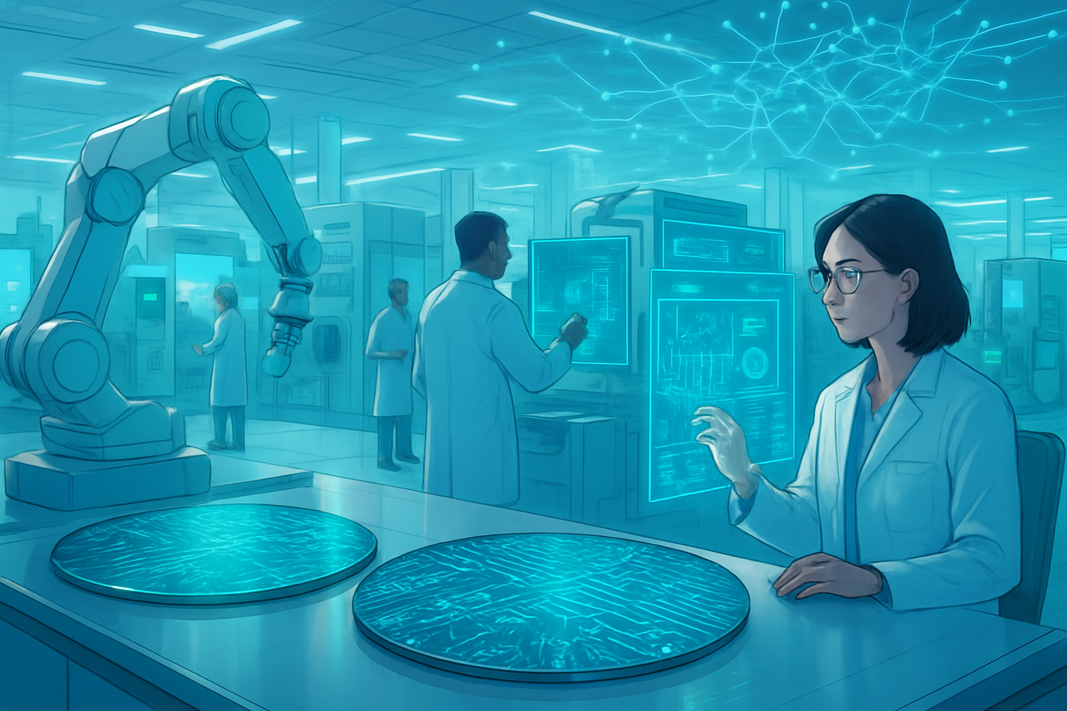
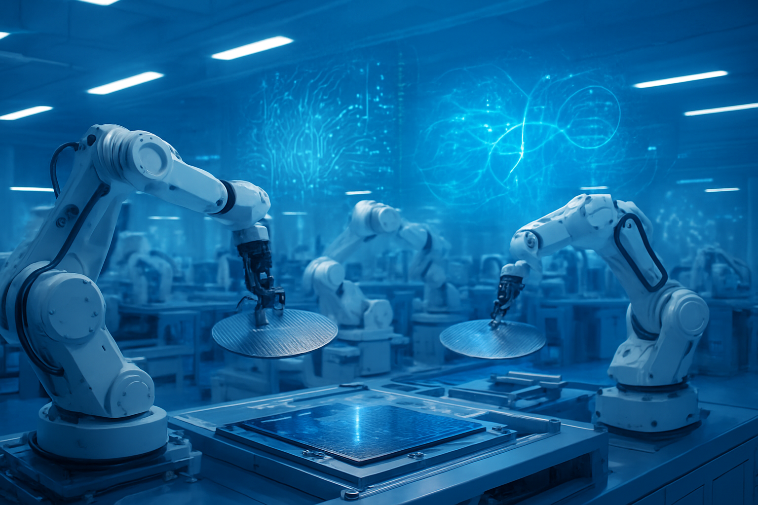
    The fabless model's technical prowess lies in its ability to foster extreme specialization. Fabless companies, such as NVIDIA Corporation (NASDAQ: NVDA), Advanced Micro Devices, Inc. (NASDAQ: AMD), Broadcom Inc. (NASDAQ: AVGO), Qualcomm Incorporated (NASDAQ: QCOM), MediaTek Inc. (TPE: 2454), and Apple Inc. (NASDAQ: AAPL), focus entirely on the intricate art of chip architecture and design. This involves defining chip functions, optimizing performance objectives, and creating detailed blueprints using sophisticated Electronic Design Automation (EDA) tools. By leveraging proprietary designs alongside off-the-shelf intellectual property (IP) cores, they craft highly optimized silicon for specific AI workloads. Once designs are finalized, they are sent to pure-play foundries like Taiwan Semiconductor Manufacturing Company (NYSE: TSM), Samsung Foundry (KRX: 005930), and GlobalFoundries Inc. (NASDAQ: GFS), which possess the advanced equipment and processes to manufacture these designs on silicon wafers.

    As of late 2025, this model is driving significant technical advancements. The industry is aggressively pursuing smaller process nodes, with 5nm, 3nm, and 2nm technologies becoming standard or entering mass production for high-performance AI chips. TSMC is leading the charge with trial production of its 2nm process using Gate-All-Around (GAA) transistor architecture, aiming for mass production in the latter half of 2025. This miniaturization allows for more transistors per chip, leading to faster, smaller, and more energy-efficient processors crucial for the explosive growth of generative AI. Beyond traditional scaling, advanced packaging technologies are now paramount. Techniques like chiplets, 2.5D packaging (e.g., TSMC's CoWoS), and 3D stacking (connected by Through-Silicon Vias or TSVs) are overcoming Moore's Law limitations by integrating multiple dies—logic, high-bandwidth memory (HBM), and even co-packaged optics (CPO)—into a single, high-performance package. This dramatically increases interconnect density and bandwidth, vital for the memory-intensive demands of AI.

    The distinction from traditional Integrated Device Manufacturers (IDMs) like Intel Corporation (NASDAQ: INTC) (though Intel is now adopting a hybrid foundry model) is stark. IDMs control the entire vertical chain from design to manufacturing, requiring colossal capital investments in fabs and process technology development. Fabless companies, conversely, avoid these direct manufacturing capital costs, allowing them to reinvest more heavily in design innovation and access the most cutting-edge process technologies developed by foundries. This horizontal specialization grants fabless firms greater agility and responsiveness to market shifts. The AI research community and industry experts largely view this fabless model as an indispensable enabler, recognizing that the "AI Supercycle" is driven by an insatiable demand for computational power that only specialized, rapidly innovated chips can provide. AI-powered EDA tools, such as Synopsys' (NASDAQ: SNPS) DSO.ai and Cadence Design Systems' (NASDAQ: CDNS) Cerebrus, are further compressing design cycles, accelerating the race for next-generation AI silicon.

    Reshaping the AI Competitive Landscape

    The fabless semiconductor model is fundamentally reshaping the competitive dynamics for AI companies, tech giants, and startups alike. Leading fabless chip designers like NVIDIA, with its dominant position in AI accelerators, and AMD, rapidly gaining ground with its MI300 series, are major beneficiaries. They can focus intensely on designing high-performance GPUs and custom SoCs optimized for AI workloads, leveraging the advanced manufacturing capabilities of foundries without the financial burden of owning fabs. This strategic advantage allows them to maintain leadership in specialized AI hardware, which is critical for training and deploying large AI models.

    Pure-play foundries, especially TSMC, are arguably the biggest winners in this scenario. TSMC's near-monopoly in advanced nodes (projected to exceed 90% in sub-5nm by 2025) grants it immense pricing power. The surging demand for AI chips has led to accelerated production schedules and significant price increases, particularly for advanced nodes and packaging technologies like CoWoS, which can increase costs for downstream companies. This concentration of manufacturing power creates a critical reliance on these foundries, prompting tech giants to secure long-term capacity and even explore in-house chip design. Companies like Alphabet Inc.'s (NASDAQ: GOOGL) Google (with its TPUs), Amazon.com Inc.'s (NASDAQ: AMZN) Amazon (with Trainium/Inferentia), Microsoft Corporation (NASDAQ: MSFT) (with Maia 100), and Meta Platforms, Inc. (NASDAQ: META) are increasingly designing their own custom AI silicon. This "in-house" trend allows them to optimize chips for proprietary AI workloads, reduce dependency on external suppliers, and potentially gain cost advantages, challenging the market share of traditional fabless leaders.

    For AI startups, the fabless model significantly lowers the barrier to entry, fostering a vibrant ecosystem of innovation. Startups can focus on niche AI chip designs for specific applications, such as edge AI devices, without the prohibitive capital expenditure of building a fab. This agility enables them to bring specialized AI chips to market faster. However, the intense demand and capacity crunch for advanced nodes mean these startups often face higher prices and longer lead times from foundries. The competitive landscape is further complicated by geopolitical influences, with the "chip war" between the U.S. and China driving efforts for indigenous chip development and supply chain diversification, forcing companies to navigate not just technological competition but also strategic supply chain resilience. This dynamic environment leads to strategic partnerships and ecosystem building, as companies aim to secure advanced node capacity and integrate their AI solutions across various applications.

    A Cornerstone in the Broader AI Landscape

    The fabless semiconductor model, and its reliance on contract manufacturing, stands as a fundamental cornerstone in the broader AI landscape of late 2025, fitting seamlessly into prevailing trends while simultaneously shaping future directions. It is the hardware enabler for the "AI Supercycle," allowing for the continuous development of specialized AI accelerators and processors that power everything from cloud-based generative AI to on-device edge AI. This model's emphasis on specialization has directly fueled the shift towards purpose-built AI chips (ASICs and NPUs) alongside general-purpose GPUs, optimizing for efficiency and performance in specific AI tasks. The adoption of chiplet and 3D packaging technologies, driven by fabless innovation, is critical for integrating diverse components and overcoming traditional silicon scaling limits, essential for the performance demands of complex AI models.

    The impacts are far-reaching. Societally, the proliferation of AI chips enabled by this model is integrating AI into an ever-growing array of devices and systems, promising advancements in healthcare, transportation, and daily life. Economically, it has fueled unprecedented growth in the semiconductor industry, with the AI segment being a primary driver, projected to reach approximately $150 billion in 2025. However, this economic boom also sees value largely concentrated among a few key suppliers, creating competitive pressures and raising concerns about market volatility due to geopolitical tensions and export controls. Technologically, the model fosters rapid advancement, not just in chip design but also in manufacturing, with AI-driven Electronic Design Automation (EDA) tools drastically reducing design cycles and AI enhancing manufacturing processes through predictive maintenance and real-time optimization.

    However, significant concerns persist. The geographic concentration of advanced semiconductor manufacturing, particularly in East Asia, creates a major supply chain vulnerability susceptible to geopolitical tensions, natural disasters, and unforeseen disruptions. The "chip war" between the U.S. and China has made semiconductors a geopolitical flashpoint, driving efforts for indigenous chip development and supply chain diversification through initiatives like the U.S. CHIPS and Science Act. While these efforts aim for resilience, they can lead to market fragmentation and increased production costs. Compared to previous AI milestones, which often focused on software breakthroughs (e.g., expert systems, machine learning algorithms, transformer architecture), the current era, enabled by the fabless model, marks a critical shift towards hardware. It's the ability to translate these algorithmic advances into tangible, high-performance, and energy-efficient hardware that distinguishes this period, making dedicated silicon infrastructure as critical as software for realizing AI's widespread potential.

    The Horizon: What Comes Next for Fabless AI

    Looking ahead from late 2025, the fabless semiconductor model, contract manufacturing, and AI chip design are poised for a period of dynamic evolution. In the near term (2025-2027), we can expect intensified specialization and customization of AI accelerators, with a continued reliance on advanced packaging solutions like chiplets and 3D stacking to achieve higher integration density and performance. AI-powered EDA tools will become even more ubiquitous, drastically cutting design timelines and optimizing power, performance, and area (PPA) for complex AI chip designs. Strategic partnerships between fabless companies, foundries, and IP providers will deepen to navigate advanced node manufacturing and secure supply chain resilience amidst ongoing capacity expansion and regionalization efforts by foundries. The global foundry capacity is forecasted to grow significantly, with Mainland China projected to hold 30% of global capacity by 2030.

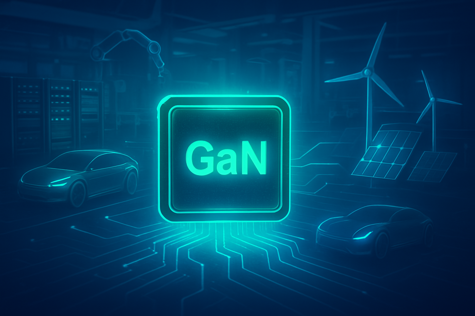
    Longer term (2028 and beyond), the trend of heterogeneous and vertical scaling will become standard for advanced data center computing and high-performance applications, disaggregating System-on-Chips (SoCs) into specialized chiplets. Research into materials beyond silicon, such as carbon and Gallium Nitride (GaN), will continue, promising more efficient power conversion. Experts predict the rise of "AI that Designs AI" by 2026, leading to modular and self-adaptive AI ecosystems. Neuromorphic computing, inspired by the human brain, is expected to gain significant traction for ultra-low power edge computing, robotics, and real-time decision-making, potentially powering 30% of edge AI devices by 2030. Beyond this, "Physical AI," encompassing autonomous robots and humanoids, will require purpose-built chipsets and sustained production scaling.

    Potential applications on the horizon are vast. Near-term, AI-enabled PCs and smartphones integrating Neural Processing Units (NPUs) are set for a significant market kick-off in 2025, transforming devices with on-device AI and personalized companions. Smart manufacturing, advanced automotive systems (especially EVs and autonomous driving), and the expansion of AI infrastructure in data centers will heavily rely on these advancements. Long-term, truly autonomous systems, advanced healthcare devices, renewable energy systems, and even space-grade semiconductors will be powered by increasingly efficient and intelligent AI chips. Challenges remain, including the soaring costs and capital intensity of advanced node manufacturing, persistent geopolitical tensions and supply chain vulnerabilities, a significant shortage of skilled engineers, and the critical need for robust power and thermal management solutions for ever more powerful AI chips. Experts predict a "semiconductor supercycle" driven by AI, with global semiconductor revenues potentially exceeding $1 trillion by 2030, largely due to AI transformation.

    A Defining Era for AI Hardware

    The fabless semiconductor model, underpinned by its essential reliance on specialized contract manufacturing, has unequivocally ushered in a defining era for AI hardware innovation. This strategic separation has proven to be the most effective mechanism for fostering rapid advancements in AI chip design, allowing companies to hyper-focus on intellectual property and architectural breakthroughs without the crippling capital burden of fabrication facilities. The synergistic relationship with leading foundries, which pour billions into cutting-edge process nodes (like TSMC's 2nm) and advanced packaging solutions, has enabled the creation of the powerful, energy-efficient AI accelerators that are indispensable for the current "AI Supercycle."

    The significance of this development in AI history cannot be overstated. It has democratized access to advanced manufacturing, allowing a diverse ecosystem of companies—from established giants like NVIDIA and AMD to nimble AI startups—to innovate at an unprecedented pace. This "design-first, factory-second" approach has been instrumental in translating theoretical AI breakthroughs into tangible, high-performance computing capabilities that are now permeating every sector of the global economy. The long-term impact will be a continuously accelerating cycle of innovation, driving the proliferation of AI into more sophisticated applications and fundamentally reshaping industries. However, this future also necessitates addressing critical vulnerabilities, particularly the geographic concentration of advanced manufacturing and the intensifying geopolitical competition for technological supremacy.

    In the coming weeks and months, several key indicators will shape this evolving landscape. Watch closely for the operational efficiency and ramp-up of TSMC's 2nm (N2) process node, expected by late 2025, and the performance of its new overseas facilities. Intel Foundry Services' progress with its 18A process and its ability to secure additional high-profile AI chip contracts will be a critical gauge of competition in the foundry space. Further innovations in advanced packaging technologies, beyond current CoWoS solutions, will be crucial for overcoming future bottlenecks. The ongoing impact of government incentives, such as the CHIPS Act, on establishing regional manufacturing hubs and diversifying the supply chain will be a major strategic development. Finally, observe the delicate balance between surging AI chip demand and supply dynamics, as any significant shifts in foundry pricing or inventory builds could signal changes in the market's current bullish trajectory. The fabless model remains the vital backbone, and its continued evolution will dictate the future pace and direction of AI itself.


    This content is intended for informational purposes only and represents analysis of current AI developments.

    TokenRing AI delivers enterprise-grade solutions for multi-agent AI workflow orchestration, AI-powered development tools, and seamless remote collaboration platforms.
    For more information, visit https://www.tokenring.ai/.

  • Forging the Future: ManpowerGroup and Maricopa Colleges Ignite Semiconductor Talent Pipeline for AI Era

    Forging the Future: ManpowerGroup and Maricopa Colleges Ignite Semiconductor Talent Pipeline for AI Era

    PHOENIX, AZ – November 11, 2025 – In a landmark move poised to reshape the landscape of advanced manufacturing and fuel the relentless advance of artificial intelligence, ManpowerGroup (NYSE: MAN) and the Maricopa Community Colleges today announced a strategic partnership. This collaboration aims to cultivate a robust pipeline of skilled talent for the rapidly expanding semiconductor industry, directly addressing a critical workforce shortage that threatens to bottleneck innovation in AI and other high-tech sectors. The initiative, centered in Arizona, is designed to provide rapid, industry-aligned training, creating direct pathways to high-demand careers and bolstering the nation's technological competitiveness.

    This strategic alliance comes at a pivotal moment, as the global demand for advanced semiconductors—the foundational hardware for nearly all AI applications—continues to surge. By uniting ManpowerGroup's expertise in workforce solutions and talent strategy with Maricopa Community Colleges' extensive educational infrastructure, the partnership seeks to deliver scalable and inclusive training programs. The immediate goal is to prepare an additional 300 individuals for careers as semiconductor technicians in Arizona, with a broader vision to train thousands more in the coming years, ensuring a steady flow of skilled workers for new and expanding fabrication plants.

    Technical Foundations: Rapid-Response Training for a High-Tech Future

    The ManpowerGroup and Maricopa Community Colleges partnership is characterized by its pragmatic, industry-driven approach to workforce development, offering a suite of programs tailored to accelerate individuals into semiconductor manufacturing roles. At the forefront are the Semiconductor Technician Quick Start program and the newly launched Maricopa Accelerated Semiconductor Training (MAST) program, complemented by more extensive academic pathways like Certificates of Completion (CCL) and an Associate in Applied Science (AAS) in Semiconductor Manufacturing.

    The Quick Start program is a prime example of this accelerated approach. This intensive 10-day course provides essential, hands-on learning in industrial technology specifically for the semiconductor industry. Its curriculum covers critical areas such as electrical theory, circuits, schematics, proper use of hand tools for maintenance, stringent workplace safety practices, clean room protocols and gowning, model-based problem solving (MBPS), lean manufacturing, and vacuum technology. Students engage with mechatronics training stations and delve into the chemistry and physics of vacuum technology. Designed for individuals with no prior experience, it culminates in an industry-relevant certification and college credits, successfully attracting a diverse demographic including people of color and first-generation college students. The MAST program, supported by a $1.7 million grant from the NSTC Workforce Partners Alliance by Natcast, aims to further expand these offerings with similar accelerated, industry-aligned content. Longer-term CCL and AAS programs provide more in-depth scientific principles and practical skills for those seeking broader career advancement.

    This collaborative model significantly diverges from traditional, often slower, educational paradigms. Its key differentiators include rapid, industry-informed curricula co-created with major employers like Intel (NASDAQ: INTC) and Taiwan Semiconductor Manufacturing Company (NYSE: TSM), ensuring direct alignment with real-time job requirements. The emphasis on hands-on, practical training, including clean room simulations and equipment troubleshooting, directly prepares students for the demanding realities of a fabrication plant. By offering compressed learning periods and direct connections to hiring employers, the partnership acts as a vital conduit, rapidly bridging the critical skills gap. While specific reactions from the AI research community were not immediately available, the broader industry and government response has been overwhelmingly positive, with government officials endorsing Quick Start as a national model and major semiconductor companies actively collaborating to address the urgent labor shortage.

    Catalyzing Growth: Impact on AI Companies, Tech Giants, and Startups

    The strategic partnership between ManpowerGroup and Maricopa Community Colleges holds profound implications for AI companies, tech giants, and startups alike. The availability of a highly skilled workforce in semiconductor manufacturing is not merely an operational convenience; it is a foundational pillar for the continued acceleration and innovation within the entire technology ecosystem, particularly in AI.

    For leading AI companies and major tech giants such as NVIDIA (NASDAQ: NVDA), Intel (NASDAQ: INTC), Samsung Electronics (KRX: 005930), TSMC (NYSE: TSM), Google (NASDAQ: GOOGL), Meta (NASDAQ: META), and Microsoft (NASDAQ: MSFT), a steady supply of talent capable of designing, manufacturing, and operating cutting-edge chips is non-negotiable. The existing skills gap has intensified the talent war, driving up labor costs and potentially delaying the development and deployment of next-generation AI hardware. This partnership directly aims to alleviate these pressures, ensuring the efficient operation of multi-billion-dollar fabrication plants, thereby reducing operational costs and accelerating innovation in AI hardware, from generative AI chips to high-performance computing accelerators. Companies like Intel, as an explicit partner, stand to directly benefit from a pipeline of technicians trained to their specific standards, while TSMC, which faced delays in its Arizona factory due to worker shortages, will find a much-needed local talent boost.

    The competitive landscape is also set to shift. A larger, better-trained talent pool can ease the intense competition for semiconductor professionals, potentially lowering recruitment costs and making it easier for companies of all sizes to find necessary expertise. This directly translates into increased innovation capacity and faster product development cycles, leading to quicker breakthroughs in AI capabilities. While dominant players like NVIDIA currently hold a strong lead in AI hardware, an improved talent pipeline could enable competitors like AMD (NASDAQ: AMD) and emerging startups focused on niche AI silicon to become more competitive, fostering a more diversified and dynamic market. This initiative primarily serves as a positive disruption, mitigating the negative impacts of talent shortages by accelerating the development of more powerful and efficient AI chips, potentially leading to faster AI advancements and more affordable AI hardware across the board.

    Broader Horizons: AI's Infrastructure and Societal Resonance

    The ManpowerGroup and Maricopa Community Colleges partnership transcends local workforce development; it is a critical investment in the very infrastructure that underpins the global AI revolution. This initiative directly addresses the foundational requirement for advanced AI: the sophisticated hardware that powers it. The relentless demand for processing speed and energy efficiency, driven by increasingly complex AI models like large language models, has created an insatiable need for specialized semiconductors—a demand that cannot be met without a robust and skilled manufacturing workforce.

    This partnership fits squarely into the broader AI landscape by tackling the most tangible bottleneck to AI progress: the physical production of its enabling technology. While AI milestones have historically focused on algorithmic breakthroughs (e.g., Deep Blue, deep learning, generative AI), this initiative represents a crucial foundational enabling milestone. It's not an AI breakthrough in itself, but rather a vital investment in the human capital necessary to design, build, and maintain the "picks and shovels" of the AI gold rush. Without a sufficient supply of advanced semiconductors and the skilled workforce to produce them, even the most innovative AI algorithms cannot be developed, trained, or deployed at scale. This effort reinforces Arizona's strategic goal of becoming a prominent semiconductor and advanced manufacturing hub, directly supporting national CHIPS Act objectives and bolstering the U.S.'s competitive advantage in the global race for AI leadership.

    The societal impacts are far-reaching and largely positive. The programs create accessible pathways to high-paying, high-tech careers, fostering economic growth and opportunity for diverse populations. By enabling AI advancements, the initiative indirectly contributes to tools that can automate repetitive tasks, allowing human workers to focus on higher-value activities. However, potential concerns include the broader trend of AI-driven job displacement, necessitating continuous reskilling efforts, and the massive energy consumption of AI data centers and manufacturing processes, which raises significant environmental challenges. The ethical implications of widespread AI adoption—such as bias, privacy, and accountability—also remain critical considerations that must be addressed in parallel with technological progress.

    The Road Ahead: Anticipating Future AI and Workforce Evolution

    The strategic partnership between ManpowerGroup and Maricopa Community Colleges marks a significant step, but it is merely the beginning of a sustained effort to secure the future of semiconductor manufacturing and, by extension, the advancement of AI. Near-term developments will see the continued expansion of programs like Quick Start and MAST, with Maricopa Community Colleges aiming to train between 4,000 and 6,000 semiconductor technicians in the coming years. ManpowerGroup will closely monitor key metrics, including enrollment numbers, job placement rates, and the continued engagement of major industry players.

    Looking further ahead, the long-term vision for the semiconductor talent pipeline is one of continuous evolution and expansion. Experts predict the global semiconductor industry will need over one million additional skilled workers by 2030, with the U.S. facing a deficit of up to 146,000 workers by 2029. This necessitates diversified talent sourcing, continuous upskilling and reskilling programs, and robust strategic workforce planning. Governments and industry will continue their collaborative efforts, driven by initiatives like the U.S. CHIPS and Science Act, to bolster domestic manufacturing and research. In parallel, AI hardware itself will continue its rapid evolution, with near-term developments focusing on even more specialized AI chips (NPUs, TPUs), an "arms race" in High-Bandwidth Memory (HBM), and the increased integration of AI into chip design and manufacturing processes for optimization.

    On the horizon, five to ten years out, we can expect transformative advancements such as photonic computing, in-memory computing, and neuromorphic computing, which promise significant gains in speed and energy efficiency for AI workloads. Quantum computing, while nascent, holds the potential for revolutionary AI processing. These hardware innovations, coupled with a highly trained workforce, will unlock advanced applications in autonomous systems, smart manufacturing, edge AI, healthcare, and clean energy. However, challenges persist: the intensifying talent shortage, the need to keep pace with rapid technological change, the high costs of innovation, the energy consumption of AI, and geopolitical risks all demand ongoing attention. Experts predict that AI will augment human engineers rather than replace them, creating new roles in managing complex AI and automated systems. The future of AI will increasingly hinge on hardware innovation, with a strong emphasis on sustainable practices and ethical considerations. The ability to identify, recruit, and develop the necessary workforce cannot rely on historical methods, making partnerships like this critical for sustained progress.

    A New Era: Securing AI's Foundation

    The partnership between ManpowerGroup and Maricopa Community Colleges represents a critical inflection point in the narrative of artificial intelligence. While AI often captures headlines with its dazzling algorithmic breakthroughs and ever-more sophisticated models, the truth remains that these advancements are fundamentally tethered to the physical world—to the silicon chips that power them. This collaboration is a powerful testament to the understanding that securing the future of AI means first securing the human talent capable of building its very foundation.

    This initiative's significance in AI history is not as a new algorithm or a computational feat, but as a vital, pragmatic investment in the human capital and infrastructure that will enable countless future AI milestones. It addresses a real-world constraint—the skilled labor shortage—that, left unchecked, could severely impede the pace of innovation. By creating accessible, accelerated pathways to high-tech careers, it not only strengthens the domestic semiconductor supply chain but also fosters economic opportunity and diversity within a crucial industry. As the demand for AI continues its exponential climb, the long-term impact of such partnerships will be measured in the resilience of our technological ecosystem, the speed of our innovation, and the inclusivity of our workforce.

    In the coming weeks and months, the tech world will be watching closely as these programs scale. Key indicators will include enrollment numbers, job placement rates, and the continued engagement of major industry players. The success of this model in Arizona could well serve as a blueprint for similar initiatives nationwide, signaling a collective commitment to building a robust, future-ready workforce for the AI era. The message is clear: the future of AI is not just about smarter algorithms, but about smarter strategies for developing the talent that brings those algorithms to life.


    This content is intended for informational purposes only and represents analysis of current AI developments.

    TokenRing AI delivers enterprise-grade solutions for multi-agent AI workflow orchestration, AI-powered development tools, and seamless remote collaboration platforms.
    For more information, visit https://www.tokenring.ai/.

  • Tower Semiconductor Soars: AI Data Center Demand Fuels Unprecedented Growth and Stock Surge

    Tower Semiconductor Soars: AI Data Center Demand Fuels Unprecedented Growth and Stock Surge

    Tower Semiconductor (NASDAQ: TSEM) is currently experiencing a remarkable period of expansion and investor confidence, with its stock performance surging on the back of a profoundly positive outlook. This ascent is not merely a fleeting market trend but a direct reflection of the company's strategic positioning within the burgeoning artificial intelligence (AI) and high-speed data center markets. As of November 10, 2025, Tower Semiconductor has emerged as a critical enabler of the AI supercycle, with its specialized foundry services, particularly in silicon photonics (SiPho) and silicon germanium (SiGe), becoming indispensable for the next generation of AI infrastructure.

    The company's recent financial reports underscore this robust trajectory, with third-quarter 2025 results exceeding analyst expectations and an optimistic outlook projected for the fourth quarter. This financial prowess, coupled with aggressive capacity expansion plans, has propelled Tower Semiconductor's valuation to new heights, nearly doubling its market value since the Intel acquisition attempt two years prior. The semiconductor industry, and indeed the broader tech landscape, is taking notice of Tower's pivotal role in supplying the foundational technologies that power the ever-increasing demands of AI.

    The Technical Backbone: Silicon Photonics and Silicon Germanium Drive AI Revolution

    At the heart of Tower Semiconductor's current success lies its mastery of highly specialized process technologies, particularly Silicon Photonics (SiPho) and Silicon Germanium (SiGe). These advanced platforms are not just incremental improvements; they represent a fundamental shift in how data is processed and transmitted within AI and high-speed data center environments, offering unparalleled performance, power efficiency, and scalability.

    Tower's SiPho platform, exemplified by its PH18 offering, is purpose-built for high-volume photonics foundry applications crucial for data center interconnects. Technically, this platform integrates low-loss silicon and silicon nitride waveguides, advanced Mach-Zehnder Modulators (MZMs), and efficient on-chip heater elements, alongside integrated Germanium PIN diodes. A significant differentiator is its support for an impressive 200 Gigabits per second (Gbps) per lane, enabling current 1.6 Terabits per second (Tbps) products and boasting a clear roadmap to 400 Gbps per lane for future 3.2 Tbps optical modules. This capability is critical for hyperscale data centers, as it dramatically reduces the number of external optical components, often halving the lasers required per module, thereby simplifying design, improving cost-efficiency, and streamlining the supply chain for AI applications. Unlike traditional electrical interconnects, SiPho offers optical solutions that inherently provide higher bandwidth and lower power consumption, a non-negotiable requirement for the ever-growing demands of AI workloads. The transition towards co-packaged optics (CPO), where the optical interface is integrated closer to the compute unit, is a key trend enabled by SiPho, fundamentally transforming the switching layer in AI networks.

    Complementing SiPho, Tower's Silicon Germanium (SiGe) BiCMOS (Bipolar-CMOS) platform is optimized for high-frequency wireless communications and high-speed networking. This technology features SiGe Heterojunction Bipolar Transistors (HBTs) with remarkable Ft/Fmax speeds exceeding 340/450 GHz, offering ultra-low noise and high linearity vital for RF applications. Tower's popular SBC18H5 SiGe BiCMOS process is particularly suited for optical fiber transceiver components like Trans-impedance Amplifiers (TIAs) and Laser Drivers (LDs), supporting data rates up to 400Gb/s and beyond, now being adopted for next-generation 800 Gb/s data networks. SiGe's ability to offer significantly lower power consumption and higher integration compared to alternative materials like Gallium Arsenide (GaAs) makes it ideal for beam-forming ICs in 5G, satellite communication, and even aerospace and defense, enabling highly agile electronically steered antennas (ESAs) that displace bulkier mechanical counterparts.

    Initial reactions from the AI research community and industry experts, as of November 2025, have been overwhelmingly positive. Tower Semiconductor's aggressive expansion into AI-focused production using these technologies has garnered significant investor confidence, leading to a surge in its valuation. Experts widely acknowledge Tower's market leadership in SiGe and SiPho for optical transceivers as critical for AI and data centers, predicting continued strong demand. Analysts view Tower as having a competitive edge over even larger players like TSMC (TPE: 2330) and Intel (NASDAQ: INTC), who are also venturing into photonics, due to Tower's specialized focus and proven capabilities. The substantial revenue growth in the SiPho segment, projected to double again in 2025 after tripling in 2024, along with strategic partnerships with companies like Innolight and Alcyon Photonics, further solidify Tower's pivotal role in the AI and high-speed data revolution.

    Reshaping the AI Landscape: Beneficiaries, Competitors, and Disruption

    Tower Semiconductor's burgeoning success in Silicon Photonics (SiPho) and Silicon Germanium (SiGe) is sending ripples throughout the AI and semiconductor industries, fundamentally altering the competitive dynamics and offering unprecedented opportunities for various players. As of November 2025, Tower's impressive $10 billion valuation, driven by its strategic focus on AI-centric production, highlights its pivotal role in providing the foundational technologies that underpin the next generation of AI computing.

    The primary beneficiaries of Tower's advancements are hyperscale data center operators and cloud providers, including tech giants like Alphabet (NASDAQ: GOOGL) (with its TPUs), Amazon (NASDAQ: AMZN) (with Inferentia and Trainium), and Microsoft (NASDAQ: MSFT). These companies are heavily investing in custom AI chips and infrastructure, and Tower's SiPho and SiGe technologies provide the critical high-speed, energy-efficient interconnects necessary for their rapidly expanding AI-driven data centers. Optical transceiver manufacturers, such as Innolight, are also direct beneficiaries, leveraging Tower's SiPho platform to mass-produce next-generation optical modules (400G/800G, 1.6T, and future 3.2T), gaining superior performance, cost efficiency, and supply chain resilience. Furthermore, a burgeoning ecosystem of AI hardware innovators and startups like Luminous Computing, Lightmatter, Celestial AI, Xscape Photonics, Oriole Networks, and Salience Labs are either actively using or poised to benefit from Tower's advanced foundry services. These companies are developing groundbreaking AI computers and accelerators that rely on silicon photonics to eliminate data movement bottlenecks and reduce power consumption, leveraging Tower's open SiPho platform to bring their innovations to market. Even NVIDIA (NASDAQ: NVDA), a dominant force in AI GPUs, is exploring silicon photonics and co-packaged optics, signaling the industry's collective shift towards these advanced interconnect solutions.

    Competitively, Tower Semiconductor's specialization creates a distinct advantage. While general-purpose foundries and tech giants like Intel (NASDAQ: INTC) and TSMC (TPE: 2330) are also entering the photonics arena, Tower's focused expertise and market leadership in SiGe and SiPho for optical transceivers provide a significant edge. Companies that continue to rely on less optimized, traditional electrical interconnects risk being outmaneuvered, as the superior energy efficiency and bandwidth offered by photonic and SiGe solutions become increasingly crucial for managing the escalating power consumption of AI workloads. This trend also reinforces the move by tech giants to develop their own custom AI chips, creating a symbiotic relationship where they still rely on specialized foundry partners like Tower for critical components.

    The potential for disruption to existing products and services is substantial. Tower's technologies directly address the "power wall" and data movement bottlenecks that have traditionally limited the scalability and performance of AI. By enabling ultra-high bandwidth and low-latency communication with significantly reduced power consumption, SiPho and SiGe allow AI systems to achieve unprecedented capabilities, potentially disrupting the cost structures of operating large AI data centers. The simplified design and integration offered by Tower's platforms—for instance, reducing the number of external optical components and lasers—streamlines the development of high-speed interconnects, making advanced AI infrastructure more accessible and efficient. This fundamental shift also paves the way for entirely new AI architectures, blurring the lines between computing, communication, and sensing, and enabling novel AI products and services that are not currently feasible with conventional technologies. Tower's aggressive capacity expansion and strategic partnerships further solidify its market positioning at the core of the AI supercycle.

    A New Era for AI Infrastructure: Broader Impacts and Paradigm Shifts

    Tower Semiconductor's breakthroughs in Silicon Photonics (SiPho) and Silicon Germanium (SiGe) extend far beyond its balance sheet, marking a significant inflection point in the broader AI landscape and the future of computational infrastructure. As of November 2025, the company's strategic investments and technological leadership are directly addressing the most pressing challenges facing the exponential growth of artificial intelligence: data bottlenecks and energy consumption.

    The wider significance of Tower's success lies in its ability to overcome the "memory wall" – the critical bottleneck where traditional electrical interconnects can no longer keep pace with the processing power of modern AI accelerators like GPUs. By leveraging light for data transmission, SiPho and SiGe provide inherently faster, more energy-efficient, and scalable solutions for connecting CPUs, GPUs, memory units, and entire data centers. This enables unprecedented data throughput, reduced power consumption, and smaller physical footprints, allowing hyperscale data centers to operate more efficiently and economically while supporting the insatiable demands of large language models (LLMs) and generative AI. Furthermore, these technologies are paving the way for entirely new AI architectures, including advancements in neuromorphic computing and high-speed optical I/O, blurring the lines between computing, communication, and sensing. Beyond data centers, the high integration, low cost, and compact size of SiPho, due to its CMOS compatibility, are crucial for emerging AI applications such as LiDAR sensors in autonomous vehicles and quantum photonic computing.

    However, this transformative potential is not without its considerations. The development and scaling of advanced fabrication facilities for SiPho and SiGe demand substantial capital expenditure and R&D investment, a challenge Tower is actively addressing with its $300-$350 million capacity expansion plan. The inherent technical complexity of heterogeneously integrating optical and electrical components on a single chip also presents ongoing engineering hurdles. While Tower holds a leadership position, it operates in a fiercely competitive market against major players like TSMC (TPE: 2330) and Intel (NASDAQ: INTC), who are also investing heavily in photonics. Furthermore, the semiconductor industry's susceptibility to global supply chain disruptions remains a persistent concern, and the substantial capital investments could become a short-term risk if the anticipated demand for these advanced solutions does not materialize as expected. Beyond the hardware layer, the broader AI ecosystem continues to grapple with challenges such as data quality, bias mitigation, lack of in-house expertise, demonstrating clear ROI, and navigating complex data privacy and regulatory compliance.

    Comparing this to previous AI milestones reveals a significant paradigm shift. While earlier breakthroughs often centered on algorithmic advancements (e.g., expert systems, backpropagation, Deep Blue, AlphaGo), or the foundational theories of AI, Tower's current contributions focus on the physical infrastructure necessary to truly unleash the power of these algorithms. This era marks a move beyond simply scaling transistor counts (Moore's Law) towards overcoming physical and economic limitations through innovative heterogeneous integration and the use of photonics. It emphasizes building intelligence more directly into physical systems, a hallmark of the "AI supercycle." This focus on the interconnect layer is a crucial next step to fully leverage the computational power of modern AI accelerators, potentially enabling neuromorphic photonic systems to achieve PetaMac/second/mm2 processing speeds, leading to ultrafast learning and significantly expanding AI applications.

    The Road Ahead: Innovations and Challenges on the Horizon

    The trajectory of Tower Semiconductor's Silicon Photonics (SiPho) and Silicon Germanium (SiGe) technologies points towards a future where data transfer is faster, more efficient, and seamlessly integrated, profoundly impacting the evolution of AI. As of November 2025, the company's aggressive roadmap and strategic investments signal a period of continuous innovation, albeit with inherent challenges.

    In the near-term (2025-2027), Tower's SiPho platform is set to push the boundaries of data rates, with a clear roadmap to 400 Gbps per lane, enabling 3.2 Terabits per second (Tbps) optical modules. This will be coupled with enhanced integration and efficiency, further reducing external optical components and halving the required lasers per module, thereby simplifying design and improving cost-effectiveness for AI and data center applications. Collaborations with partners like OpenLight are expected to bring hybrid integrated laser versions to market, further solidifying SiPho's capabilities. For SiGe, near-term developments focus on continued optimization of high-speed transistors with Ft/Fmax speeds exceeding 340/450 GHz, ensuring ultra-low noise and high linearity for advanced RF applications, and supporting bandwidths up to 800 Gbps systems, with advancements towards 1.6 Tbps. Tower's 300mm wafer process, upgrading from its existing 200mm production, will allow for monolithic integration of SiPho with CMOS and SiGe BiCMOS, streamlining production and enhancing performance.

    Looking into the long-term (2028-2030 and beyond), the industry is bracing for widespread adoption of Co-Packaged Optics (CPO), where optical transceivers are integrated directly with switch ASICs or processors, bringing the optical interface closer to the compute unit. This will offer unmatched customization and scalability for AI infrastructure. Tower's SiPho platform is a key enabler of this transition. For SiGe, long-term advancements include 3D integration of SiGe layers in stacked architectures for enhanced device performance and miniaturization, alongside material innovations to further improve its properties for even higher performance and new functionalities.

    These technologies unlock a myriad of potential applications and use cases. SiPho will remain crucial for AI and data center interconnects, addressing the "memory wall" and energy consumption bottlenecks. Its role will expand into high-performance computing (HPC), emerging sensor applications like LiDAR for autonomous vehicles, and eventually, quantum computing and neuromorphic systems that mimic the human brain's neural structure for more energy-efficient AI. SiGe, meanwhile, will continue to be vital for high-speed communication within AI infrastructure, optical fiber transceiver components, and advanced wireless applications like 5G, 6G, and satellite communications (SatCom), including low-earth orbit (LEO) constellations. Its low-power, high-frequency capabilities also make it ideal for edge AI and IoT devices.

    However, several challenges need to be addressed. The integration complexity of combining optical components with existing electronic systems, especially in CPO, remains a significant technical hurdle. High R&D costs, although mitigated by leveraging established CMOS fabrication and economies of scale, will persist. Managing power and thermal aspects in increasingly dense AI systems will be a continuous engineering challenge. Furthermore, like all global foundries, Tower Semiconductor is susceptible to geopolitical challenges, trade restrictions, and supply chain disruptions. Operational execution risks also exist in converting and repurposing fabrication capacities.

    Despite these challenges, experts are highly optimistic. The silicon photonics market is projected for rapid growth, reaching over $8 billion by 2030, with a Compound Annual Growth Rate (CAGR) of 25.8%. Analysts see Tower as leading rivals in SiPho and SiGe production, holding over 50% market share in Trans-impedance Amplifiers (TIAs) and drivers for datacom optical transceivers. The company's SiPho segment revenue, which tripled in 2024 and is expected to double again in 2025, underscores this confidence. Industry trends, including the shift from AI model training to inference and the increasing adoption of CPO by major players like NVIDIA (NASDAQ: NVDA), further validate Tower's strategic direction. Experts predict continued aggressive investment by Tower in capacity expansion and R&D through 2025-2026 to meet accelerating demand from AI, data centers, and 5G markets.

    Tower Semiconductor: Powering the AI Supercycle's Foundation

    Tower Semiconductor's (NASDAQ: TSEM) journey, marked by its surging stock performance and positive outlook, is a testament to its pivotal role in the ongoing artificial intelligence supercycle. The company's strategic mastery of Silicon Photonics (SiPho) and Silicon Germanium (SiGe) technologies has not only propelled its financial growth but has also positioned it as an indispensable enabler for the next generation of AI and high-speed data infrastructure.

    The key takeaways are clear: Tower is a recognized leader in SiGe and SiPho for optical transceivers, demonstrating robust financial growth with its SiPho revenue tripling in 2024 and projected to double again in 2025. Its technological innovations, such as the 200 Gbps per lane SiPho platform with a roadmap to 3.2 Tbps, and SiGe BiCMOS with over 340/450 GHz Ft/Fmax speeds, are directly addressing the critical bottlenecks in AI data processing. The company's commitment to aggressive capacity expansion, backed by an additional $300-$350 million investment, underscores its intent to meet escalating demand. A significant breakthrough involves technology that dramatically reduces external optical components and halves the required lasers per module, enhancing cost-efficiency and supply chain resilience.

    In the grand tapestry of AI history, Tower Semiconductor's contributions represent a crucial shift. It signifies a move beyond traditional transistor scaling, emphasizing heterogeneous integration and photonics to overcome the physical and economic limitations of current AI hardware. By enabling ultra-fast, energy-efficient data communication, Tower is fundamentally transforming the switching layer in AI networks and driving the transition to Co-Packaged Optics (CPO). This empowers not just tech giants but also fosters innovation among AI companies and startups, diversifying the AI hardware landscape. The significance lies in providing the foundational infrastructure that allows the complex algorithms of modern AI, especially generative AI, to truly flourish.

    Looking at the long-term impact, Tower's innovations are set to guide the industry towards a future where optical and high-frequency analog components are seamlessly integrated with digital processing units. This integration is anticipated to pave the way for entirely new AI architectures and capabilities, further blurring the lines between computing, communication, and sensing. With ambitious long-term goals of achieving $2.7 billion in annual revenues, Tower's strategic focus on high-value analog solutions and robust partnerships are poised to sustain its success in powering the next generation of AI.

    In the coming weeks and months, investors and industry observers should closely watch Tower Semiconductor's Q4 2025 financial results, which are projected to show record revenue. The execution and impact of its substantial capacity expansion investments across its fabs will be critical. Continued acceleration of SiPho revenue, the transition towards CPO, and concrete progress on 3.2T optical modules will be key indicators of market adoption. Finally, new customer engagements and partnerships, particularly in advanced optical module production and RF infrastructure growth, will signal the ongoing expansion of Tower's influence in the AI-driven semiconductor landscape. Tower Semiconductor is not just riding the AI wave; it's building the surfboard.


    This content is intended for informational purposes only and represents analysis of current AI developments.

    TokenRing AI delivers enterprise-grade solutions for multi-agent AI workflow orchestration, AI-powered development tools, and seamless remote collaboration platforms.
    For more information, visit https://www.tokenring.ai/.

  • GlobalFoundries and TSMC Forge Landmark GaN Alliance, Reshaping US Power Chip Manufacturing

    GlobalFoundries and TSMC Forge Landmark GaN Alliance, Reshaping US Power Chip Manufacturing

    In a pivotal development set to redefine the landscape of power semiconductor manufacturing, GlobalFoundries (NASDAQ: GFS) announced on November 10, 2025, a significant technology licensing agreement with Taiwan Semiconductor Manufacturing Company (NYSE: TSM). This strategic partnership focuses on advanced Gallium Nitride (GaN) technology, specifically 650V and 80V platforms, and is poised to dramatically accelerate GlobalFoundries' development and U.S.-based production of next-generation GaN power chips. The immediate significance lies in fortifying the domestic supply chain for critical power components, addressing burgeoning demand across high-growth sectors.

    This collaboration emerges at a crucial juncture, as TSMC, a global foundry leader, prepares to strategically exit its broader GaN foundry services by July 2027 to intensify its focus on advanced-node silicon for AI applications and advanced packaging. GlobalFoundries' acquisition of this proven GaN expertise not only ensures the continued availability and advancement of the technology but also strategically positions its Burlington, Vermont, facility as a vital hub for U.S.-manufactured GaN semiconductors, bolstering national efforts towards semiconductor independence and resilience.

    Technical Prowess: Unpacking the Advanced GaN Technology

    The licensed technology from TSMC encompasses both 650V and 80V GaN-on-Silicon (GaN-on-Si) capabilities. GlobalFoundries will leverage its existing high-voltage GaN-on-Silicon expertise at its Burlington facility to integrate and scale this technology, with a strong focus on 200mm (8-inch) wafer manufacturing for high-volume production. This move is particularly impactful as TSMC had previously developed robust second-generation GaN-on-Si processes, and GlobalFoundries is now gaining access to this established and validated technology.

    GaN technology offers substantial performance advantages over traditional silicon-based semiconductors in power applications due to its wider bandgap. Key differentiators include significantly higher energy efficiency and power density, enabling smaller, more compact designs. GaN devices boast faster switching speeds—up to 10 times faster than silicon MOSFETs and 100 times faster than IGBTs—which allows for higher operating frequencies and smaller passive components. Furthermore, GaN exhibits superior thermal performance, efficiently dissipating heat and reducing the need for complex cooling systems.

    Unlike previous approaches that relied heavily on silicon, which is reaching its performance limits in terms of efficiency and power density, GaN provides a critical leap forward. While Silicon Carbide (SiC) is another wide bandgap material, GaN-on-Silicon offers a cost-effective solution for operating voltages below 1000V by utilizing existing silicon manufacturing infrastructure. Initial reactions from the semiconductor research community and industry experts have been largely positive, viewing this as a strategic win for GlobalFoundries and a significant step towards strengthening the U.S. domestic semiconductor ecosystem, especially given TSMC's strategic pivot.

    The technology is targeted for high-performance, energy-efficient applications across various sectors, including power management solutions for data centers, industrial power applications, and critical components for electric vehicles (EVs) such as onboard chargers and DC-DC converters. It also holds promise for renewable energy systems, fast-charging electronics, IoT devices, and even aerospace and defense applications requiring robust RF and high-power control. GlobalFoundries emphasizes a holistic approach to GaN reliability, designing for harsh environments to ensure robustness and longevity.

    Market Ripple Effects: Impact on the Semiconductor Industry

    This strategic partnership carries profound implications for semiconductor companies, tech giants, and startups alike. GlobalFoundries (NASDAQ: GFS) stands as the primary beneficiary, gaining rapid access to proven GaN technology that will significantly accelerate its GaN roadmap and bolster its position as a leading contract manufacturer. This move allows GF to address the growing demand for higher efficiency and power density in power systems, offering a crucial U.S.-based manufacturing option for GaN-on-silicon semiconductors.

    For other semiconductor companies, the landscape is shifting. Companies that previously relied on TSMC (NYSE: TSM) for GaN foundry services, such as Navitas Semiconductor (NASDAQ: NVTS) and ROHM (TSE: 6963), have already begun seeking alternative manufacturing partners due to TSMC's impending exit. GlobalFoundries, with its newly acquired technology and planned U.S. production, is now poised to become a key alternative foundry, potentially capturing a significant portion of this reallocated business. This intensifies competition for established players like Infineon Technologies (OTC: IFNNY) and Innoscience, which are also major forces in the power semiconductor and GaN markets.

    Tech giants involved in cloud computing, electric vehicles, and advanced industrial equipment stand to benefit from a more diversified and robust GaN supply chain. The increased manufacturing capacity and technological expertise at GlobalFoundries will lead to a wider availability of GaN power devices, enabling these companies to integrate more energy-efficient and compact designs into their products. For startups focused on innovative GaN-based power management solutions, GlobalFoundries' entry provides a reliable manufacturing partner, potentially lowering barriers to entry and accelerating time-to-market.

    The primary disruption stems from TSMC's withdrawal from GaN foundry services, which necessitates a transition for its current GaN customers. However, GlobalFoundries' timely entry with licensed TSMC technology can mitigate some of this disruption by offering a familiar and proven process. This development significantly bolsters U.S.-based manufacturing capabilities for advanced semiconductors, enhancing market positioning and strategic advantages for GlobalFoundries by offering U.S.-based GaN capacity to a global customer base, aligning with national initiatives to strengthen domestic chip production.

    Broader Significance: A New Era for Power Electronics

    The GlobalFoundries and TSMC GaN technology licensing agreement signifies a critical juncture in the broader semiconductor manufacturing landscape, underscoring a decisive shift towards advanced materials and enhanced supply chain resilience. This partnership accelerates the adoption of GaN, a "third-generation" semiconductor material, which offers superior performance characteristics over traditional silicon, particularly in high-power and high-frequency applications. Its ability to deliver higher efficiency, faster switching speeds, and better thermal management is crucial as silicon-based CMOS technologies approach their fundamental limits.

    This move fits perfectly into current trends driven by the surging demand from next-generation technologies such as 5G telecommunications, electric vehicles, data centers, and renewable energy systems. The market for GaN semiconductor devices is projected for substantial growth, with some estimates predicting the power GaN market to reach approximately $3 billion by 2030. The agreement's emphasis on establishing U.S.-based GaN capacity directly addresses pressing concerns about supply chain resilience, especially given the geopolitical sensitivity surrounding raw materials like gallium. Diversifying manufacturing locations for critical components is a top priority for national security and economic stability.

    The impacts on global chip production are multifaceted. It promises increased availability and competition in the GaN market, offering customers an additional U.S.-based manufacturing option that could reduce lead times and geopolitical risks. This expanded capacity will enable more widespread integration of GaN into new product designs across various industries, leading to more efficient and compact electronic systems. While intellectual property (IP) is always a concern in such agreements, the history of cross-licensing and cooperation between TSMC and GlobalFoundries suggests a framework for managing such issues, allowing both companies freedom to operate and innovate.

    Comparisons to previous semiconductor industry milestones are apt. This shift from silicon to GaN for specific applications mirrors the earlier transition from germanium to silicon in the early days of transistors, driven by superior material properties. It represents a "vertical" advancement in material capability, distinct from the "horizontal" scaling achieved through lithography advancements, promising to enable new generations of power-efficient devices. This strategic collaboration also highlights the industry's evolving approach to IP, where licensing agreements facilitate technological progress rather than being bogged down by disputes.

    The Road Ahead: Future Developments and Challenges

    The GlobalFoundries and TSMC GaN partnership heralds significant near-term and long-term developments for advanced GaN power chips. In the near term, development of the licensed technology is slated to commence in early 2026 at GlobalFoundries' Burlington, Vermont facility, with initial production expected to ramp up later that year. This rapid integration aims to quickly bring high-performance GaN solutions to market, leveraging GlobalFoundries' existing expertise and significant federal funding (over $80 million since 2020) dedicated to advancing GaN-on-silicon manufacturing in the U.S.

    Long-term, the partnership is set to deliver GaN chips that will address critical power gaps across mission-critical applications in data centers, automotive, and industrial sectors. The comprehensive GaN portfolio GlobalFoundries is developing, designed for harsh environments and emphasizing reliability, will solidify GaN's role as a next-generation solution for achieving higher efficiency, power density, and compactness where traditional silicon CMOS technologies approach their limits.

    Potential applications and use cases for these advanced GaN power chips are vast and transformative. In Artificial Intelligence (AI), GaN is crucial for meeting the exponential energy demands of AI data centers, enabling power supplies to evolve for higher computational power within reduced footprints. For Electric Vehicles (EVs), GaN promises extended range and faster charging capabilities through smaller, lighter, and more efficient power conversion systems in onboard chargers and DC-DC converters, with future potential in traction inverters. In Renewable Energy, GaN will enhance energy conversion efficiency in solar inverters, wind turbine systems, and overall grid infrastructure, contributing to grid stability and decarbonization efforts.

    Despite its promising future, GaN technology faces challenges, particularly concerning U.S.-based manufacturing capabilities. These include the higher initial cost of GaN components, the complexities of manufacturing scalability and yield (such as lattice mismatch defects when growing GaN on silicon), and ensuring long-term reliability in harsh operating environments. A critical challenge for the U.S. is the current lack of sufficient domestic epitaxy capacity, a crucial step in GaN production, necessitating increased investment to secure the supply chain.

    Experts predict a rapid expansion of the GaN market, with significant growth projected through 2030 and beyond, driven by AI and electrification. GaN is expected to displace legacy silicon in many high-power applications, becoming ubiquitous in power conversion stages from consumer devices to grid-scale energy storage. Future innovations will focus on increased integration, with GaN power FETs combined with control, drive, sensing, and protection circuitry into single, high-performance GaN ICs. The transition to larger wafer sizes (300mm) and advancements in vertical GaN technology are also anticipated to further enhance efficiency and cost-effectiveness.

    A New Chapter in US Chip Independence

    The GlobalFoundries and TSMC GaN technology licensing agreement marks a monumental step, not just for the companies involved, but for the entire semiconductor industry and the broader global economy. The key takeaway is the strategic acceleration of U.S.-based GaN manufacturing, driven by a world-class technology transfer. This development is profoundly significant in the context of semiconductor manufacturing history, representing a critical shift towards advanced materials and a proactive approach to supply chain resilience.

    Its long-term impact on U.S. chip independence and technological advancement is substantial. By establishing a robust domestic hub for advanced GaN production at GlobalFoundries' Vermont facility, the U.S. gains greater control over the manufacturing of essential components for strategic sectors like defense, electric vehicles, and renewable energy. This not only enhances national security but also fosters innovation within the U.S. semiconductor ecosystem, driving economic growth and creating high-tech jobs.

    In the coming weeks and months, industry observers and consumers should closely watch for GlobalFoundries' qualification and production milestones at its Vermont facility in early 2026, followed by the availability of initial products later that year. Monitor customer adoption and design wins, particularly in the data center, industrial, and automotive sectors, as these will be crucial indicators of market acceptance. Keep an eye on the evolving GaN market pricing and competition, especially with TSMC's exit and the continued pressure from other global players. Finally, continued U.S. government support and broader technological advancements in GaN, such as larger wafer sizes and new integration techniques, will be vital to watch for as this partnership unfolds and shapes the future of power electronics.


    This content is intended for informational purposes only and represents analysis of current AI developments.

    TokenRing AI delivers enterprise-grade solutions for multi-agent AI workflow orchestration, AI-powered development tools, and seamless remote collaboration platforms.
    For more information, visit https://www.tokenring.ai/.

  • Valens Semiconductor Ignites Medical Imaging Revolution with VA7000-Powered Endoscopes

    Valens Semiconductor Ignites Medical Imaging Revolution with VA7000-Powered Endoscopes

    Valens Semiconductor (NYSE: VLN), a pioneer in high-speed connectivity solutions, has announced its groundbreaking entry into the medical imaging market, heralding a new era for endoscopic procedures. The company's innovative VA7000 chipset, originally designed for the rigorous demands of the automotive industry, is now powering next-generation endoscopes, promising to enhance patient safety, improve diagnostic accuracy, and streamline surgical workflows. This strategic expansion positions Valens at the forefront of a significant shift towards advanced, high-resolution, and increasingly disposable medical devices, addressing critical needs within the healthcare sector.

    The immediate significance of this development lies in its potential to revolutionize the landscape of medical endoscopy. By enabling the creation of advanced disposable endoscopes, the VA7000 chipset directly tackles the long-standing challenges associated with the sterilization and reprocessing of reusable endoscopes, which have historically posed infection risks and operational burdens. This move is not merely an incremental improvement but a foundational step towards safer, more efficient, and higher-quality patient care, with implications for hospitals, clinics, and ultimately, patients worldwide.

    A Technical Leap Forward in Endoscopic Imaging

    The Valens VA7000 series is a MIPI A-PHY-compliant Serializer/Deserializer (SerDes) chipset, a testament to robust engineering initially honed for automotive applications like Advanced Driver-Assistance Systems (ADAS). Its transition to medical imaging underscores the VA7000's exceptional capabilities, which are now being leveraged to meet the stringent demands of surgical environments. Key technical specifications and features that make the VA7000 a game-changer include its support for multi-gigabit connectivity, enabling high-resolution video up to 4K over ultra-thin coaxial and Unshielded Twisted Pair (UTP) cables. This capability is paramount for endoscopes, where maneuverability and crystal-clear visualization are non-negotiable.

    Crucially, the VA7000 distinguishes itself with built-in electrosurgical noise cancellation. This feature is vital in operating rooms where electromagnetic interference from electrosurgical units can severely degrade video quality. By ensuring stable, artifact-free images even during complex procedures, the VA7000 enhances a surgeon's ability to make precise decisions. Furthermore, its small form factor and low power consumption are optimized for miniaturization, allowing for more compact camera modules within endoscopes—a critical factor for single-use devices—and reducing heat generation at the tip. The chipset's exceptional Electromagnetic Compatibility (EMC) reliability, inherited from its automotive-grade design, guarantees consistent performance in electrically noisy medical environments.

    Unlike previous approaches that often required complex in-camera image signal processing (ISP) or compromised on image quality for smaller form factors, the VA7000 simplifies the system architecture. It can potentially remove the need for an ISP within the camera module itself, centralizing image processing at the receiver and allowing for a significantly more compact and cost-effective camera design. Initial reactions from the medical device industry have been overwhelmingly positive, with three Original Equipment Manufacturers (OEMs) already launching VA7000-powered products, including an innovative laparoscope, a 3D imaging solution for robotic surgeries, and the first single-use colonoscope with 4K video resolution. This rapid adoption signals strong validation from medical experts and a clear demand for the advanced capabilities offered by Valens.

    Reshaping the Competitive Landscape of Medical Technology

    Valens Semiconductor's (NYSE: VLN) foray into medical imaging with the VA7000 chipset is poised to significantly impact various players across the AI and semiconductor industries, as well as the broader medical technology sector. Valens itself stands to gain immensely from this strategic expansion, tapping into a lucrative new market with substantial growth potential. The annual Total Addressable Market (TAM) for single-use endoscopes alone is projected to reach hundreds of millions of dollars, with the broader disposable endoscope market expected to grow into billions by 2030. This provides a robust new revenue stream and diversifies Valens' market presence beyond its traditional automotive strongholds.

    For medical device OEMs, the VA7000 acts as a critical enabler. Companies developing endoscopes can now create products with superior image quality, enhanced safety features, and simplified designs, potentially accelerating their time to market and strengthening their competitive edge. This development could disrupt traditional manufacturers of reusable endoscopes, who face increasing pressure from regulatory bodies like the U.S. FDA to mitigate infection risks. The shift towards disposable solutions, facilitated by technologies like the VA7000, may force these incumbents to innovate rapidly or risk losing market share to agile competitors leveraging new connectivity standards.

    Furthermore, this advancement has implications for AI companies and startups specializing in medical image analysis and computer vision. With the VA7000 enabling higher resolution (4K) and more stable video feeds, the quality of data available for AI training and real-time diagnostic assistance dramatically improves. This could lead to more accurate AI-powered detection of anomalies, better surgical guidance systems, and new opportunities for AI-driven surgical robotics. Valens' market positioning is strengthened as a foundational technology provider, becoming an indispensable partner for companies aiming to integrate advanced imaging and AI into next-generation medical devices.

    Broader Significance and Societal Impact

    Valens Semiconductor's entry into the medical imaging market with the VA7000 chipset is more than just a product launch; it represents a significant milestone within the broader AI and medical technology landscape. This development aligns perfectly with several prevailing trends: the increasing demand for miniaturization in medical devices, the push for single-use instruments to enhance patient safety, and the relentless pursuit of higher-resolution imaging for improved diagnostic accuracy. By providing a robust, high-speed, and interference-resistant connectivity solution, the VA7000 removes a critical technical barrier that previously hindered the widespread adoption of advanced disposable endoscopy architectures.

    The impact on patient safety is perhaps the most profound. The U.S. FDA has actively advocated for single-use endoscopes to reduce the risk of healthcare-associated infections (HAIs) linked to inadequately reprocessed reusable devices. The VA7000 directly facilitates this transition by making high-performance disposable endoscopes economically and technically viable, potentially saving lives and reducing the significant costs associated with treating HAIs. Improved clinical outcomes are also a direct benefit; higher resolution, stable video feeds, and wider fields of view empower medical professionals with better visualization, leading to more precise diagnoses and more accurate surgical interventions.

    While the benefits are substantial, potential concerns might include the environmental impact of increased disposable medical waste, although this must be weighed against the severe risks of infection from reusable devices. Compared to previous AI milestones, such as the development of advanced diagnostic algorithms, the VA7000 represents a foundational hardware breakthrough that enables these AI applications to reach their full potential. It ensures that the AI models receive the highest quality, most reliable data stream from within the human body, bridging the gap between cutting-edge sensor technology and intelligent processing.

    The Horizon of Future Medical Innovations

    The introduction of Valens Semiconductor's (NYSE: VLN) VA7000 into medical imaging endoscopes sets the stage for a wave of exciting future developments in healthcare technology. In the near term, we can expect to see a rapid proliferation of new disposable endoscopic devices across various medical specialties, leveraging the VA7000's capabilities for 4K imaging, 3D visualization, and enhanced maneuverability. This will likely extend beyond colonoscopes and laparoscopes to bronchoscopes, ureteroscopes, and other minimally invasive instruments, making advanced procedures safer and more accessible.

    Longer term, the VA7000's robust connectivity will be crucial for integrating these advanced endoscopes with artificial intelligence and machine learning systems. Experts predict a future where AI-powered algorithms provide real-time diagnostic assistance during procedures, highlighting suspicious areas, measuring tissue characteristics, and even guiding robotic surgical tools with unprecedented precision. The high-quality, stable data stream provided by the VA7000 is fundamental for training and deploying these sophisticated AI models effectively. We could also see the emergence of "smart" endoscopes that incorporate additional sensors for chemical analysis, temperature mapping, or even localized drug delivery, all communicating via the VA7000's high-speed link.

    However, challenges remain. Widespread adoption will depend on balancing the cost-effectiveness of disposable solutions with the capital expenditures required for new processing units and the ongoing operational costs. Regulatory hurdles, although somewhat mitigated by the FDA's stance on disposables, will still need careful navigation for new device types. What experts predict next is a continued convergence of hardware innovation, like the VA7000, with advanced AI software, leading to a new generation of intelligent, highly capable, and safer medical instruments that will fundamentally transform diagnostic and surgical practices over the next decade.

    A New Era for Intelligent Medical Imaging

    Valens Semiconductor's (NYSE: VLN) strategic entry into the medical imaging market with its VA7000-powered endoscopes marks a pivotal moment in the evolution of healthcare technology. The key takeaway is the enablement of high-performance, disposable endoscopes that address critical issues of patient safety, diagnostic accuracy, and operational efficiency. By repurposing its robust automotive-grade MIPI A-PHY SerDes chipset, Valens has provided the foundational connectivity layer necessary for a new generation of medical devices, characterized by 4K resolution, electrosurgical noise cancellation, and a compact, low-power design.

    This development holds significant historical importance in AI and medical technology, as it directly facilitates the widespread adoption of advanced imaging critical for future AI-driven diagnostics and robotic surgery. It is a testament to how specialized hardware innovation can unlock the full potential of software-based intelligence. The long-term impact is profound, promising safer surgical environments, more precise medical interventions, and potentially lower healthcare costs by reducing infection rates and streamlining procedures.

    In the coming weeks and months, the industry will be closely watching the market penetration of the initial VA7000-powered endoscopes and the reactions from healthcare providers. We can anticipate further announcements from medical device OEMs adopting this technology, alongside increasing interest from AI companies looking to integrate their advanced analytics with these superior imaging capabilities. Valens Semiconductor has not just entered a new market; it has laid down a critical piece of infrastructure for the intelligent operating rooms of the future.


    This content is intended for informational purposes only and represents analysis of current AI developments.

    TokenRing AI delivers enterprise-grade solutions for multi-agent AI workflow orchestration, AI-powered development tools, and seamless remote collaboration platforms.
    For more information, visit https://www.tokenring.ai/.

  • Silicon’s Struggle: A Global Race to Bridge the Semiconductor Skills Gap

    Silicon’s Struggle: A Global Race to Bridge the Semiconductor Skills Gap

    The global semiconductor industry, a foundational pillar of modern technology and a critical enabler for the burgeoning AI revolution, finds itself at a pivotal crossroads in late 2025. While demand for advanced chips soars, fueled by innovations in artificial intelligence, electric vehicles, and data centers, a severe and escalating skills gap threatens to derail this unprecedented growth. Governments and industry leaders worldwide are now engaged in a frantic, multi-faceted effort to cultivate a robust advanced manufacturing workforce, recognizing that a failure to do so could have profound implications for economic competitiveness, national security, and the pace of technological advancement. This concerted push aims not just to fill immediate vacancies but to fundamentally reshape the talent pipeline for an industry projected to reach a trillion-dollar valuation by 2030.

    Unpacking the Workforce Crisis: Technical Solutions and Strategic Shifts

    The semiconductor workforce crisis is characterized by both a quantitative and qualitative deficit. Projections indicate a need for over one million additional skilled workers globally by 2030, with the U.S. alone potentially facing a shortfall of up to 300,000 skilled workers in the same timeframe. This isn't merely a numbers game; the industry demands highly specialized expertise in cutting-edge areas like extreme ultraviolet (EUV) lithography, 3D chip stacking, advanced packaging, and the integration of AI and machine learning into manufacturing processes. Roles from technicians (projected 39% shortfall in the U.S.) to master's and PhD-level engineers (26% shortfall) are acutely affected, highlighting a systemic issue fueled by an aging workforce, an insufficient educational pipeline, intense competition for STEM talent, and the rapid evolution of manufacturing technologies.

    In response, a wave of strategic initiatives and technical solutions is being deployed, marking a significant departure from previous, often fragmented, workforce development efforts. A cornerstone of this new approach in the United States is the CHIPS and Science Act of 2022, which, by 2025, has already allocated nearly $300 million in dedicated workforce funds to support over 25 CHIPS-funded manufacturing facilities across 12 states. Crucially, it has also invested $250 million in the National Semiconductor Technology Center (NSTC) Workforce Center of Excellence. The NSTC, with a symposium expected in September 2025, is establishing a Technical Advisory Board to guide curriculum development and workforce standards, focusing on grants for projects that train technicians—a role accounting for roughly 60% of new positions and requiring less than a bachelor's degree. This targeted investment in vocational and associate-level training represents a significant shift towards practical, job-ready skills, differing from past reliance solely on four-year university pipelines.

    Beyond federal legislation, the current landscape is defined by unprecedented collaboration between industry, academia, and government. Over 50 community colleges have either launched or expanded semiconductor-related programs, often in direct partnership with major chipmakers like Intel Corporation (NASDAQ: INTC), Taiwan Semiconductor Manufacturing Company (NYSE: TSM), Samsung Electronics Co., Ltd. (KRX: 005930), and Micron Technology, Inc. (NASDAQ: MU). These companies, as part of their CHIPS Act awards, have committed substantial funds to workforce development, establishing apprenticeships, "earn-and-learn" programs, and specialized bootcamps. Furthermore, 14 states have collectively committed over $300 million in new funding, often incentivized by the CHIPS Program Office, to foster local talent ecosystems. The integration of AI and automation is also playing a dual role: creating new mission-critical skills requirements while simultaneously being leveraged for recruitment, skills assessment, and personalized training to streamline workforce development and accelerate upskilling, a stark contrast to older, more manual training methodologies. This multi-pronged, collaborative strategy is designed to create a more agile and responsive talent pipeline capable of adapting to the industry's rapid technological advancements.

    Corporate Giants and Nimble Startups: Navigating the Talent Tsunami

    The escalating semiconductor skills gap has profound implications for every player in the tech ecosystem, from established tech giants and major AI labs to burgeoning startups. At its core, the ability to secure and cultivate a highly specialized workforce is rapidly becoming the ultimate strategic advantage in an industry where human capital directly translates into innovation capacity and market leadership.

    Leading semiconductor manufacturers, the very backbone of the digital economy, are at the forefront of this impact. Companies like Intel Corporation (NASDAQ: INTC), Taiwan Semiconductor Manufacturing Company (NYSE: TSM), Samsung Electronics Co., Ltd. (KRX: 005930), Micron Technology, Inc. (NASDAQ: MU), and GlobalFoundries (NASDAQ: GFS) are not merely recipients of government incentives but active participants in shaping the future workforce. Their substantial investments in training programs, collaborations with educational institutions (such as Arizona State University and Maricopa Community Colleges), and establishment of state-of-the-art training facilities are crucial. These efforts, often amplified by funding from initiatives like the U.S. CHIPS and Science Act, provide a direct competitive edge by securing a pipeline of talent essential for operating and expanding new fabrication plants (fabs). Without skilled engineers and technicians, these multi-billion-dollar investments risk underutilization, leading to delayed product development and increased operational costs.

    For major AI labs and tech giants like NVIDIA Corporation (NASDAQ: NVDA), whose dominance in AI hardware is predicated on advanced chip design and manufacturing, the skills gap translates into an intensified talent war. The scarcity of professionals proficient in areas like AI-specific chip architecture, machine learning integration, and advanced process technologies drives up compensation and benefits, raising the barrier to entry for smaller players. Companies that can effectively attract and retain this elite talent gain a significant strategic advantage in the race for AI supremacy. Conversely, startups, particularly those focused on novel AI hardware or specialized silicon, face an existential challenge. Without the deep pockets of their larger counterparts, attracting highly specialized chip designers and manufacturing experts becomes incredibly difficult, potentially stifling groundbreaking innovation at its earliest stages and creating an imbalance where promising AI hardware concepts struggle to move from design to production.

    The potential for disruption to existing products and services is considerable. A persistent talent shortage can lead to significant delays in product development and rollout, particularly for advanced AI applications requiring custom silicon. This can slow the pace of innovation across the entire tech sector. Moreover, the scarcity of talent drives up labor costs, which can translate into higher overall production costs for electronics and AI hardware, potentially impacting consumer prices and profit margins. However, this challenge is also catalyzing innovation in workforce management. Companies are increasingly leveraging AI and automation not just in manufacturing, but in recruitment, skills assessment, and personalized training. This redefines job roles, augmenting human capabilities and allowing engineers to focus on higher-value tasks, thereby enhancing productivity and offering a strategic advantage to those who effectively integrate these tools into their human capital strategies. The market positioning of tech firms is thus increasingly defined not just by their intellectual property or capital, but by their ability to cultivate and leverage a highly skilled workforce, making human capital the new battleground for competitive differentiation.

    Wider Significance: A Geopolitical Imperative and AI's Foundation

    The concerted global effort to bridge the semiconductor skills gap transcends mere industry economics; it represents a critical geopolitical imperative and a foundational challenge for the future of artificial intelligence. Semiconductors are the bedrock of virtually every modern technology, from smartphones and autonomous vehicles to advanced weaponry and the vast data centers powering AI. A robust, domestically controlled semiconductor workforce is therefore inextricably linked to national security, economic sovereignty, and technological leadership in the 21st century.

    This current push fits squarely into a broader global trend of reshoring and regionalizing critical supply chains, a movement significantly accelerated by recent geopolitical tensions and the COVID-19 pandemic. Governments, particularly in the U.S. (with the CHIPS and Science Act) and Europe (with the European Chips Act), are investing hundreds of billions to boost domestic chip production and reduce reliance on a highly concentrated East Asian supply chain. However, these massive capital investments in new fabrication plants will yield little without the human talent to design, build, and operate them. The skills gap thus becomes the ultimate bottleneck, threatening to undermine these strategic national initiatives. Addressing it is not just about producing more chips, but about ensuring that nations have the capacity to innovate and control their technological destiny.

    The implications for the broader AI landscape are particularly profound. The "AI supercycle" is driving unprecedented demand for specialized AI accelerators, GPUs, and custom silicon, pushing the boundaries of chip design and manufacturing. Without a sufficient pool of highly skilled engineers and technicians capable of working with advanced materials, complex lithography, and novel chip architectures, the pace of AI innovation itself could slow. This could lead to delays in developing next-generation AI models, limit the efficiency of AI systems, and potentially restrict the widespread deployment of AI-powered solutions across industries. The skills gap is, in essence, a constraint on the very foundation upon which future AI breakthroughs will be built.

    Potential concerns, however, also accompany these efforts. The intense competition for talent could exacerbate existing inequalities, with smaller companies or less affluent regions struggling to attract and retain skilled workers. There's also the risk that rapid technological advancements, particularly in AI and automation, could create a perpetual cycle of upskilling requirements, making it challenging for workforce development programs to keep pace. Comparisons to previous technological milestones, such as the space race or the early days of the internet, reveal a similar pattern: grand visions require equally grand investments in human capital. However, the current challenge is unique in its global scale and the foundational nature of the technology involved. The ability to successfully bridge this gap will not only dictate the success of national semiconductor strategies but also profoundly shape the future trajectory of AI and its transformative impact on society.

    The Road Ahead: Sustained Investment and Evolving Paradigms

    Looking beyond 2025, the trajectory of the semiconductor industry will be profoundly shaped by its ability to cultivate and sustain a robust, highly skilled workforce. Experts predict that the talent shortage, particularly for engineers and technicians, will intensify further before showing significant signs of improvement, with a global need for over one million additional skilled workers by 2030. This necessitates not just continued investment but a fundamental transformation in how talent is sourced, trained, and retained.

    In the near term (2025-2027), we can expect an accelerated surge in demand for engineers and technicians, with annual demand growth potentially doubling in some areas. This will drive an intensified focus on strategic partnerships between semiconductor companies and educational institutions, including universities, community colleges, and vocational schools. These collaborations will be crucial for developing specialized training programs, fast-track certifications, and expanding apprenticeships and internships. Companies like Intel Corporation (NASDAQ: INTC) are already pioneering accelerated training programs, such as their 10-day Quick Start Semiconductor Technician Training, which are likely to become more prevalent. Furthermore, the integration of advanced technologies like AI, digital twins, virtual reality (VR), and augmented reality (AR) into training methodologies is expected to become commonplace, boosting efficiency and accelerating learning curves for complex manufacturing processes. Government initiatives, particularly the U.S. CHIPS and Science Act and the European Chips Act, will continue to be pivotal, with their allocated funding driving significant workforce development efforts.

    Longer term (2028-2030 and beyond), the industry anticipates a more holistic workforce transformation. This will involve adapting job requirements to attract a wider talent pool and tapping into non-traditional sources. Efforts to enhance the semiconductor industry's brand image and improve diversity, equity, and inclusion (DEI) will be vital to attract a new generation of workers who might otherwise gravitate towards other tech sectors. Educational curricula will become even more tightly integrated with industry needs, ensuring graduates are job-ready for roles in advanced manufacturing and cleanroom operations. Potential applications and use cases for a well-staffed semiconductor sector are vast and critical for global progress: from accelerating breakthroughs in Artificial Intelligence (AI) and Machine Learning (ML), including generative AI chips and high-performance computing, to enabling advancements in electric vehicles, next-generation telecommunications (5G/6G), and the burgeoning Internet of Things (IoT). A skilled workforce is also foundational for cutting-edge fields like quantum computing and advanced packaging technologies.

    However, significant challenges remain. The widening talent gap, exacerbated by an aging workforce nearing retirement and persistent low industry appeal compared to other tech fields, poses a continuous threat. The rapid pace of technological change, encompassing innovations like extreme ultraviolet (EUV) lithography and 3D chip stacking, constantly shifts required skill sets, making it difficult for traditional educational pipelines to keep pace. Competition for talent from other high-growth industries like clean energy and cybersecurity is fierce. Experts predict that strategic workforce planning will remain a top priority for semiconductor executives, emphasizing talent development and retention. AI is seen as a double-edged sword: while driving demand for advanced chips, it is also expected to become a crucial tool for alleviating engineering talent shortages by streamlining operations and boosting productivity. Ultimately, the future success of the semiconductor industry will depend not only on technological advancements but critically on the human capital it can attract, develop, and retain, making the race for chip sovereignty intrinsically linked to the race for talent.

    Wrap-Up: A Defining Moment for AI's Foundation

    The global semiconductor industry stands at a defining juncture, grappling with a profound skills gap that threatens to undermine unprecedented demand and strategic national initiatives. This detailed examination reveals a critical takeaway: the future of artificial intelligence, economic competitiveness, and national security hinges on the urgent and sustained development of a robust advanced manufacturing workforce for semiconductors. The current landscape, marked by significant governmental investment through legislation like the U.S. CHIPS and Science Act, and intensified collaboration between industry and academia, represents a concerted effort to fundamentally reshape the talent pipeline.

    This development is not merely another industry trend; it is a foundational challenge that will dictate the pace of technological progress for decades to come. The ability of major players like Intel Corporation (NASDAQ: INTC), Taiwan Semiconductor Manufacturing Company (NYSE: TSM), Samsung Electronics Co., Ltd. (KRX: 005930), and Micron Technology, Inc. (NASDAQ: MU) to secure and cultivate skilled personnel will directly impact their market positioning, competitive advantage, and capacity for innovation. For AI companies and tech giants, a stable supply of human talent capable of designing and manufacturing cutting-edge chips is as critical as the capital and research itself.

    The long-term impact of successfully bridging this gap will be transformative, enabling continued breakthroughs in AI, advanced computing, and critical infrastructure. Conversely, failure to address this challenge could lead to prolonged innovation bottlenecks, increased geopolitical vulnerabilities, and economic stagnation. As we move into the coming weeks and months, watch for further announcements regarding new educational partnerships, vocational training programs, and strategic investments aimed at attracting and retaining talent. The effectiveness of these initiatives will be a crucial barometer for the industry's health and the broader trajectory of technological advancement. The race for silicon sovereignty is ultimately a race for human ingenuity and skill, and the stakes could not be higher.


    This content is intended for informational purposes only and represents analysis of current AI developments.

    TokenRing AI delivers enterprise-grade solutions for multi-agent AI workflow orchestration, AI-powered development tools, and seamless remote collaboration platforms.
    For more information, visit https://www.tokenring.ai/.

  • India’s Chip Dream Takes Shape: Tata Electronics’ Assam Plant Ignites Self-Reliance and Reshapes Global Supply Chains

    India’s Chip Dream Takes Shape: Tata Electronics’ Assam Plant Ignites Self-Reliance and Reshapes Global Supply Chains

    Jagiroad, Assam – November 7, 2025 – In a landmark development for India's ambitious drive towards semiconductor self-reliance, Union Finance Minister Nirmala Sitharaman today visited Tata Electronics' (NSE: TATAELXSI) cutting-edge semiconductor manufacturing facility in Jagiroad, Assam. Her presence underscored the national significance of this monumental project, which is poised to transform India into a crucial node in the global semiconductor supply chain and significantly bolster the nation's technological sovereignty. This greenfield Outsourced Semiconductor Assembly and Test (OSAT) unit represents a strategic leap, aiming to dramatically reduce India's historical dependence on imported chips and foster a robust, indigenous semiconductor ecosystem.

    The facility, a cornerstone of Prime Minister Narendra Modi's 'Viksit Bharat' vision, is more than just a manufacturing plant; it symbolizes India's resolve to move beyond being a consumer of technology to becoming a producer and innovator. As construction progresses rapidly, with the first phase expected to be operational by mid-2025 and full-scale production of "Made In India" chips slated for 2026, the Assam plant is set to address critical demands across diverse sectors, from electric vehicles and mobile devices to advanced AI applications and communication infrastructure.

    Engineering India's Semiconductor Future: A Deep Dive into Tata Electronics' OSAT Facility

    The Tata Electronics semiconductor facility in Jagiroad represents a staggering investment of approximately INR 27,000 crore (around US$3.6 billion), a testament to the scale of India's commitment to this high-tech sector. Approved by the Union Cabinet on February 29, 2024, and following a groundbreaking ceremony on August 3, 2024, the project has moved with remarkable speed, driven by the supportive framework of the India Semiconductor Mission and Assam's Electronics policy.

    This state-of-the-art OSAT unit will specialize in advanced packaging technologies, a critical phase in semiconductor manufacturing that involves assembling, testing, and packaging integrated circuits before they are deployed in electronic devices. The facility will initially deploy three key platform technologies: Wire Bond, Flip Chip, and Integrated Systems Packaging (ISP), with plans for a future roadmap to incorporate even more advanced packaging solutions. Once fully operational, the plant is projected to produce an impressive 4.83 crore (48.3 million) chips per day, employing indigenously developed technologies to cater to a vast array of applications including 5G communications, routers, and other consumer and industrial electronics, particularly for the burgeoning electric vehicle market.

    The establishment of such an advanced OSAT facility marks a significant departure from India's traditional role, which has historically been strong in chip design but heavily reliant on foreign manufacturing for production. By focusing on advanced packaging, Tata Electronics is not only building a crucial part of the semiconductor value chain domestically but also positioning India to capture a higher value segment. This strategic move aims to reduce the current import dependence, which stands at over 90% of India's semiconductor demand, and to build a resilient supply chain that can withstand global disruptions, distinguishing it from previous approaches that primarily focused on chip design.

    Reshaping the Competitive Landscape: Implications for Tech Giants and Startups

    The advent of Tata Electronics' (NSE: TATAELXSI) Assam plant carries profound implications for a wide spectrum of companies, from established tech giants to burgeoning startups, both domestically and internationally. Indian technology companies, particularly those in the automotive, consumer electronics, and telecommunications sectors, stand to benefit immensely from a reliable, localized source of high-quality packaged semiconductors. This domestic supply will mitigate risks associated with geopolitical tensions and global supply chain bottlenecks, offering greater stability and faster turnaround times for product development and manufacturing.

    Globally, the new OSAT facility positions India as a competitive alternative to existing semiconductor packaging hubs, predominantly located in East Asia. Companies like Apple (NASDAQ: AAPL), Samsung (KRX: 005930), and Qualcomm (NASDAQ: QCOM), which rely heavily on outsourced assembly and testing, may find India an attractive option for diversifying their supply chains, enhancing resilience, and potentially reducing costs in the long run. This development introduces a new dynamic into the competitive landscape, potentially disrupting the market positioning of established OSAT providers by offering a strategically located, high-capacity alternative.

    Furthermore, this initiative could catalyze the growth of a vibrant ecosystem of ancillary industries and startups in India. Companies involved in semiconductor design, materials, equipment, and testing services will find new opportunities for collaboration and expansion. The plant's focus on advanced packaging for sectors like AI and EVs will also fuel innovation within India's AI startups and automotive tech firms, providing them with crucial hardware components developed within the country. This strategic advantage could foster a new wave of innovation and product development, strengthening India's overall technological prowess and market share in critical global industries.

    A Pillar of India's Global Semiconductor Ambition and Geopolitical Resilience

    The Tata Electronics facility in Assam is far more than an isolated industrial project; it is a critical pillar in India's broader strategic vision to become a global semiconductor powerhouse. This endeavor is meticulously guided by the India Semiconductor Mission (ISM), launched in December 2021 with a substantial outlay of ₹76,000 crore (approximately US$10 billion), alongside the National Policy on Electronics (NPE) 2019. These policies aim to cultivate a sustainable semiconductor and display ecosystem across the entire value chain, offering attractive incentives, including the Production Linked Incentive (PLI) Scheme, to foster domestic manufacturing.

    The plant's strategic importance extends to global supply chain resilience. Amidst growing geopolitical uncertainties and the lessons learned from recent global chip shortages, nations worldwide are seeking to decentralize and diversify their semiconductor manufacturing capabilities. India, with its vast talent pool, growing market, and robust government support, is emerging as a compelling partner in this global recalibration. The "Made in Assam" chips are not only intended for domestic consumption but are also expected to be supplied to major international markets, including Japan, the United States, and Germany, thereby cementing India's role in the global technology infrastructure.

    Beyond economic benefits, the facility underscores India's commitment to strategic autonomy. By reducing its overwhelming reliance on chip imports, India enhances its national security and technological independence. This move draws parallels with efforts by other major economies, such as the United States and the European Union, to bring semiconductor manufacturing onshore. The project is expected to significantly boost industrialization in India's North-Eastern region, creating hundreds of thousands of direct and indirect jobs and contributing to holistic regional development, aligning with the vision of 'Viksit Bharat' and positioning India as a reliable and competitive player in the global technology arena.

    The Road Ahead: Cultivating a Comprehensive Semiconductor Ecosystem

    Looking ahead, the Tata Electronics (NSE: TATAELXSI) semiconductor facility in Assam is merely the beginning of a much larger journey for India. The initial focus on advanced OSAT technologies, including Wire Bond, Flip Chip, and Integrated Systems Packaging (ISP), is expected to pave the way for a broader expansion into even more sophisticated packaging solutions and potentially, over time, into more complex fabrication (fab) processes. Experts predict that the success of this and similar initiatives will embolden further investments across the semiconductor value chain, from materials and equipment manufacturing to design and R&D.

    The government's continued support through the India Semiconductor Mission and various incentive schemes will be crucial in overcoming challenges such as developing a highly skilled workforce, attracting top-tier global talent, and keeping pace with the rapid technological advancements in the semiconductor industry. Educational institutions and vocational training centers will need to align their curricula with the industry's demands, ensuring a steady supply of engineers and technicians. The collaboration between industry, academia, and government will be paramount for sustained growth.

    Experts anticipate that by the end of the decade, India's semiconductor market, projected to surge from approximately $38 billion in 2023 to $100-$110 billion by 2030, will not only cater to a significant portion of its domestic demand but also become a significant exporter of chips and related services. The success of the Assam plant will serve as a blueprint and a confidence booster for future projects, cementing India's position as a formidable force in the global semiconductor industry and a crucial contributor to the next generation of technological advancements. This development is not just about chips; it's about shaping India's future as a global leader in technology and innovation.

    A New Dawn for Indian Technology: The Long-Term Impact

    The establishment of Tata Electronics' (NSE: TATAELXSI) semiconductor manufacturing facility in Assam marks a pivotal moment in India's technological history. It signifies a decisive step towards achieving true self-reliance in a critical industry, moving beyond aspirations to concrete execution. The facility's rapid development, supported by substantial investment and robust government backing, underscores India's commitment to building a resilient and indigenous semiconductor ecosystem. This endeavor is set to not only fuel the nation's economic growth but also to fundamentally alter its strategic standing on the global stage.

    The long-term impact of this development will be multifaceted. Economically, it promises to create hundreds of thousands of high-value jobs, attract further foreign direct investment, and drive industrialization in previously underserved regions. Strategically, it will provide India with greater control over its technological destiny, reducing vulnerabilities to global supply chain shocks and geopolitical pressures. Environmentally, the focus on a "greenfield" facility emphasizes sustainable manufacturing practices, aligning with global efforts towards responsible industrial growth.

    As the plant moves towards full operational capacity in 2026, the world will be watching closely. Key milestones to watch for in the coming weeks and months include further announcements regarding technological partnerships, progress on workforce development initiatives, and the initial production runs. The success of the "Made In India" chips from Assam will undoubtedly inspire further investments and innovations, cementing India's position as a formidable force in the global semiconductor industry and a crucial contributor to the next generation of technological advancements. This development is not just about chips; it's about shaping India's future as a global leader in technology and innovation.


    This content is intended for informational purposes only and represents analysis of current AI developments.

    TokenRing AI delivers enterprise-grade solutions for multi-agent AI workflow orchestration, AI-powered development tools, and seamless remote collaboration platforms.
    For more information, visit https://www.tokenring.ai/.

  • India’s Semiconductor Dawn: Tata Electronics Plant in Assam Poised to Reshape Global Tech Landscape

    India’s Semiconductor Dawn: Tata Electronics Plant in Assam Poised to Reshape Global Tech Landscape

    GUWAHATI, ASSAM – November 7, 2025 – In a monumental stride towards technological self-reliance, India today witnessed Union Finance Minister Nirmala Sitharaman's pivotal visit to the new Tata Electronics semiconductor manufacturing facility in Jagiroad, Assam. This state-of-the-art Outsourced Semiconductor Assembly and Test (OSAT) unit, backed by an investment of INR 27,000 crore (approximately US$3.6 billion), is not merely a factory; it is a declaration of intent, positioning India at the heart of the global semiconductor supply chain and promising to ignite an economic transformation in the country's North-Eastern region. The facility, currently under construction, is on track for its first phase of operations by mid-2025, with full-scale production slated for 2026, marking a critical juncture in India's journey to becoming a formidable player in high-tech manufacturing.

    The significance of this project reverberated through Minister Sitharaman's remarks during her review of the advanced facility. She hailed the initiative as the "driver of the engine for Viksit Bharat" (Developed India) and a "golden moment" for Assam, underscoring its alignment with Prime Minister Narendra Modi's vision of a self-reliant India and the holistic development of the North-Eastern region. The establishment of such a high-value manufacturing unit is expected to dramatically reduce India's historical dependence on imported chips, fortifying its economic and strategic resilience in an increasingly digitized world.

    A Deep Dive into India's Semiconductor Ambition

    The Tata Electronics (a subsidiary of the Tata Group, represented by public entities like Tata Motors (NSE: TATAMOTORS)) facility in Assam is designed as an advanced OSAT unit, focusing on the critical stages of semiconductor manufacturing: assembly and testing. This involves taking silicon wafers produced elsewhere and transforming them into finished, functional chips through sophisticated packaging techniques. The plant will leverage three cutting-edge platform technologies: Wire Bond, Flip Chip, and Integrated Systems Packaging (ISP). These technologies are crucial for creating high-performance, compact, and reliable semiconductor components essential for modern electronics.

    Unlike traditional chip fabrication (fabs), which involves the complex and capital-intensive process of wafer manufacturing, the OSAT unit specializes in the subsequent, equally vital steps of packaging and testing. This strategic focus allows India to rapidly build capabilities in a high-value segment of the semiconductor supply chain that is currently dominated by a few global players. The semiconductors processed here will be integral to a vast array of applications, including the rapidly expanding electric vehicle (EV) sector, mobile devices, artificial intelligence (AI) hardware, advanced communications infrastructure, industrial automation, and diverse consumer electronics. Once fully operational, the facility boasts an impressive capacity to produce up to 48 million semiconductor chips daily, a testament to its scale and ambition. This indigenous capability is a stark departure from previous approaches, where India primarily served as a consumer market, and represents a significant leap in its technological maturity. Initial reactions from the domestic tech community have been overwhelmingly positive, viewing it as a watershed moment for India's manufacturing prowess.

    Reshaping the Indian and Global Tech Landscape

    The establishment of the Tata Electronics semiconductor plant is poised to have a profound impact on various stakeholders, from major tech giants to emerging startups. For the Tata Group itself, this venture marks a significant diversification and strengthening of its industrial portfolio, positioning it as a key player in a strategically vital sector. The project is expected to attract a global ecosystem to India, fostering the development of cutting-edge technologies and advanced skill sets within the country. Tata Group Chairman N Chandrasekaran had previously indicated plans to sign Memoranda of Understanding (MoUs) with ten additional semiconductor companies, signaling a concerted effort to build a robust ancillary ecosystem around the Assam facility.

    This development presents competitive implications for existing global semiconductor players by offering a new, geographically diversified manufacturing hub. While not directly competing with established fabrication giants, the OSAT facility provides an alternative for packaging and testing services, potentially reducing lead times and supply chain risks for companies worldwide. Indian tech startups, particularly those in AI, IoT, and automotive electronics, stand to benefit immensely from the domestic availability of advanced semiconductor components, enabling faster prototyping, reduced import costs, and greater innovation. The plant’s existence could also disrupt existing product development cycles by providing a localized, efficient supply of critical components, encouraging more companies to design and manufacture within India, thus enhancing the nation's market positioning and strategic advantages in the global tech arena.

    Broader Implications and Global Supply Chain Resilience

    The Tata Electronics facility in Assam fits seamlessly into the broader global trend of diversifying semiconductor manufacturing away from concentrated hubs, a strategy increasingly prioritized in the wake of geopolitical tensions and recent supply chain disruptions. By establishing significant OSAT capabilities, India is actively contributing to de-risking the global tech supply chain, offering an alternative production base that enhances resilience and reduces the world's reliance on a few key regions, particularly in East Asia. This move solidifies India's commitment to becoming a reliable and integral part of the global technology ecosystem, moving beyond its traditional role as a software and services powerhouse to a hardware manufacturing hub.

    The economic impacts on Assam and the wider North-Eastern region are anticipated to be transformative. The INR 27,000 crore investment is projected to create over 27,000 direct and indirect jobs, providing substantial employment opportunities and fostering economic diversification in a region traditionally reliant on agriculture and tea. Beyond direct employment, the project necessitates and stimulates significant infrastructure development, including improved roads, utilities, and an "electronic city" designed to house approximately 40,000 employees. The Government of Assam's commitment of a Rs 111 crore Water Supply Project further underscores the holistic development around the plant. This industrialization is expected to spawn numerous peripheral industries, creating a vibrant local business ecosystem and positioning the Northeast as a key driver in India's technology-driven growth narrative, comparable to how previous industrial milestones have reshaped other regions.

    The Road Ahead: Future Developments and Challenges

    With the first phase of the Tata Electronics plant expected to be operational by mid-2025 and full production by 2026, the near-term focus will be on ramping up operations, ensuring quality control, and integrating seamlessly into global supply chains. Experts predict that the success of this initial venture could pave the way for further significant investments in India's semiconductor ecosystem, potentially including more advanced fabrication units in the long term. The plant's focus on advanced packaging technologies like Wire Bond, Flip Chip, and ISP suggests a pathway towards even more sophisticated packaging solutions in the future, keeping pace with evolving global demands.

    However, challenges remain. Developing a highly skilled workforce capable of operating and maintaining such advanced facilities will be crucial, necessitating robust training programs and educational initiatives. Maintaining a technological edge in a rapidly evolving industry will also require continuous investment in research and development. What experts predict next is a domino effect: the establishment of this anchor unit is expected to attract more foreign direct investment into India's semiconductor sector, fostering a complete ecosystem from design to manufacturing and testing. Potential applications and use cases on the horizon include specialized chips for India's burgeoning space and defense sectors, further cementing the nation's strategic autonomy.

    A New Chapter in India's Industrial History

    The Tata Electronics semiconductor manufacturing facility in Assam represents a pivotal moment in India's industrial and technological history. It is a bold statement of intent, signaling India's ambition to move beyond being a consumer of technology to a significant producer, capable of meeting both domestic and global demands for critical electronic components. The substantial investment, coupled with the promise of thousands of jobs and comprehensive regional development, underscores the project's multifaceted significance.

    As the facility moves from construction to operationalization in the coming months, the world will be watching. The success of this venture will not only bolster India's self-reliance in a strategically vital sector but also contribute significantly to the diversification and resilience of the global tech supply chain. Key takeaways include India's commitment to indigenous manufacturing, the transformative economic potential for the North-East, and the strategic importance of semiconductor independence. The coming weeks and months will be crucial as the plant approaches its operational milestones, with further partnerships and ecosystem developments expected to unfold, cementing India's place on the global semiconductor map.


    This content is intended for informational purposes only and represents analysis of current AI developments.

    TokenRing AI delivers enterprise-grade solutions for multi-agent AI workflow orchestration, AI-powered development tools, and seamless remote collaboration platforms.
    For more information, visit https://www.tokenring.ai/.

  • RISC-V: The Open-Source Revolution Reshaping AI Hardware Innovation

    RISC-V: The Open-Source Revolution Reshaping AI Hardware Innovation

    The artificial intelligence landscape is witnessing a profound shift, driven not only by advancements in algorithms but also by a quiet revolution in hardware. At its heart is the RISC-V (Reduced Instruction Set Computer – Five) architecture, an open-standard Instruction Set Architecture (ISA) that is rapidly emerging as a transformative alternative for AI hardware innovation. As of November 2025, RISC-V is no longer a nascent concept but a formidable force, democratizing chip design, fostering unprecedented customization, and driving cost efficiencies in the burgeoning AI domain. Its immediate significance lies in its ability to challenge the long-standing dominance of proprietary architectures like Arm and x86, thereby unlocking new avenues for innovation and accelerating the pace of AI development across the globe.

    This open-source paradigm is significantly lowering the barrier to entry for AI chip development, enabling a diverse ecosystem of startups, research institutions, and established tech giants to design highly specialized and efficient AI accelerators. By eliminating the expensive licensing fees associated with proprietary ISAs, RISC-V empowers a broader array of players to contribute to the rapidly evolving field of AI, fostering a more inclusive and competitive environment. The ability to tailor and extend the instruction set to specific AI applications is proving critical for optimizing performance, power, and area (PPA) across a spectrum of AI workloads, from energy-efficient edge computing to high-performance data centers.

    Technical Prowess: RISC-V's Edge in AI Hardware

    RISC-V's fundamental design philosophy, emphasizing simplicity, modularity, and extensibility, makes it exceptionally well-suited for the dynamic demands of AI hardware.

    A cornerstone of RISC-V's appeal for AI is its customizability and extensibility. Unlike rigid proprietary ISAs, RISC-V allows developers to create custom instructions that precisely accelerate domain-specific AI workloads, such as fused multiply-add (FMA) operations, custom tensor cores for sparse models, quantization, or tensor fusion. This flexibility facilitates the tight integration of specialized hardware accelerators, including Neural Processing Units (NPUs) and General Matrix Multiply (GEMM) accelerators, directly with the RISC-V core. This hardware-software co-optimization is crucial for enhancing efficiency in tasks like image signal processing and neural network inference, leading to highly specialized and efficient AI accelerators.

    The RISC-V Vector Extension (RVV) is another critical component for AI acceleration, offering Single Instruction, Multiple Data (SIMD)-style parallelism with superior flexibility. Its vector-length agnostic (VLA) model allows the same program to run efficiently on hardware with varying vector register lengths (e.g., 128-bit to 16 kilobits) without recompilation, ensuring scalability from low-power embedded systems to high-performance computing (HPC) environments. RVV natively supports various data types essential for AI, including 8-bit, 16-bit, 32-bit, and 64-bit integers, as well as single and double-precision floating points. Efforts are also underway to fast-track support for bfloat16 (BF16) and 8-bit floating-point (FP8) data types, which are vital for enhancing the efficiency of AI training and inference. Benchmarking suggests that RVV can achieve 20-30% better utilization in certain convolutional operations compared to ARM's Scalable Vector Extension (SVE), attributed to its flexible vector grouping and length-agnostic programming.

    Modularity is intrinsic to RISC-V, starting with a fundamental base ISA (RV32I or RV64I) that can be selectively expanded with optional standard extensions (e.g., M for integer multiply/divide, V for vector processing). This "lego-brick" approach enables chip designers to include only the necessary features, reducing complexity, silicon area, and power consumption, making it ideal for heterogeneous System-on-Chip (SoC) designs. Furthermore, RISC-V AI accelerators are engineered for power efficiency, making them particularly well-suited for energy-constrained environments like edge computing and IoT devices. Some analyses indicate RISC-V can offer approximately a 3x advantage in computational performance per watt compared to ARM and x86 architectures in specific AI contexts due to its streamlined instruction set and customizable nature. While high-end RISC-V designs are still catching up to the best ARM offers, the performance gap is narrowing, with near parity projected by the end of 2026.

    Initial reactions from the AI research community and industry experts as of November 2025 are largely optimistic. Industry reports project substantial growth for RISC-V, with Semico Research forecasting a staggering 73.6% annual growth in chips incorporating RISC-V technology, anticipating 25 billion AI chips by 2027 and generating $291 billion in revenue. Major players like Google (NASDAQ: GOOGL), NVIDIA (NASDAQ: NVDA), and Samsung (KRX: 005930) are actively embracing RISC-V for various applications, from controlling GPUs to developing next-generation AI chips. The maturation of the RISC-V ecosystem, bolstered by initiatives like the RVA23 application profile and the RISC-V Software Ecosystem (RISE), is also instilling confidence.

    Reshaping the AI Industry: Impact on Companies and Competitive Dynamics

    The emergence of RISC-V is fundamentally altering the competitive landscape for AI companies, tech giants, and startups, creating new opportunities and strategic advantages.

    AI startups and smaller players are among the biggest beneficiaries. The royalty-free nature of RISC-V significantly lowers the barrier to entry for chip design, enabling agile startups to rapidly innovate and develop highly specialized AI solutions without the burden of expensive licensing fees. This fosters greater control over intellectual property and allows for bespoke implementations tailored to unique AI workloads. Companies like ChipAgents, an AI startup focused on semiconductor design and verification, recently secured a $21 million Series A round, highlighting investor confidence in this new paradigm.

    Tech giants are also strategically embracing RISC-V to gain greater control over their hardware infrastructure, reduce reliance on third-party licenses, and optimize chips for specific AI workloads. Google (NASDAQ: GOOGL) has integrated RISC-V into its Coral NPU for edge AI, while NVIDIA (NASDAQ: NVDA) utilizes RISC-V cores extensively within its GPUs for control tasks and has announced CUDA support for RISC-V, enabling it as a main processor in AI systems. Samsung (KRX: 005930) is developing next-generation AI chips based on RISC-V, including the Mach 1 AI inference chip, to achieve greater technological independence. Other major players like Broadcom (NASDAQ: AVGO), Meta (NASDAQ: META), MediaTek (TPE: 2454), Qualcomm (NASDAQ: QCOM), and Renesas (TYO: 6723) are actively validating RISC-V's utility across various semiconductor applications. Qualcomm, a leader in mobile, IoT, and automotive, is particularly well-positioned in the Edge AI semiconductor market, leveraging RISC-V for power-efficient, cost-effective inference at scale.

    The competitive implications for established players like Arm (NASDAQ: ARM) and Intel (NASDAQ: INTC) are substantial. RISC-V's open and customizable nature directly challenges the proprietary models that have long dominated the market. This competition is forcing incumbents to innovate faster and could disrupt existing product roadmaps. The ability for companies to "own the design" with RISC-V is a key advantage, particularly in industries like automotive where control over the entire stack is highly valued. The growing maturity of the RISC-V ecosystem, coupled with increased availability of development tools and strong community support, is attracting significant investment, further intensifying this competitive pressure.

    RISC-V is poised to disrupt existing products and services across several domains. In Edge AI devices, its low-power and extensible nature is crucial for enabling ultra-low-power, always-on AI in smartphones, IoT devices, and wearables, potentially making older, less efficient hardware obsolete faster. For data centers and cloud AI, RISC-V is increasingly adopted for higher-end applications, with the RVA23 profile ensuring software portability for high-performance application processors, leading to more energy-efficient and scalable cloud computing solutions. The automotive industry is experiencing explosive growth with RISC-V, driven by the demand for low-cost, highly reliable, and customizable solutions for autonomous driving, ADAS, and in-vehicle infotainment.

    Strategically, RISC-V's market positioning is strengthening due to its global standardization, exemplified by RISC-V International's approval as an ISO/IEC JTC1 PAS Submitter in November 2025. This move towards global standardization, coupled with an increasingly mature ecosystem, solidifies its trajectory from an academic curiosity to an industrial powerhouse. The cost-effectiveness and reduced vendor lock-in provide strategic independence, a crucial advantage amidst geopolitical shifts and export restrictions. Industry analysts project the global RISC-V CPU IP market to reach approximately $2.8 billion by 2025, with chip shipments increasing by 50% annually between 2024 and 2030, reaching over 21 billion chips by 2031, largely credited to its increasing use in Edge AI deployments.

    Wider Significance: A New Era for AI Hardware

    RISC-V's rise signifies more than just a new chip architecture; it represents a fundamental shift in how AI hardware is designed, developed, and deployed, resonating with broader trends in the AI landscape.

    Its open and modular nature aligns perfectly with the democratization of AI. By removing the financial and technical barriers of proprietary ISAs, RISC-V empowers a wider array of organizations, from academic researchers to startups, to access and innovate at the hardware level. This fosters a more inclusive and diverse environment for AI development, moving away from a few dominant players. This also supports the drive for specialized and custom hardware, a critical need in the current AI era where general-purpose architectures often fall short. RISC-V's customizability allows for domain-specific accelerators and tailored instruction sets, crucial for optimizing the diverse and rapidly evolving workloads of AI.

    The focus on energy efficiency for AI is another area where RISC-V shines. As AI demands ever-increasing computational power, the need for energy-efficient solutions becomes paramount. RISC-V AI accelerators are designed for minimal power consumption, making them ideal for the burgeoning edge AI market, including IoT devices, autonomous vehicles, and wearables. Furthermore, in an increasingly complex geopolitical landscape, RISC-V offers strategic independence for nations and companies seeking to reduce reliance on foreign chip design architectures and maintain sovereign control over critical AI infrastructure.

    RISC-V's impact on innovation and accessibility is profound. It lowers barriers to entry and enhances cost efficiency, making advanced AI development accessible to a wider array of organizations. It also reduces vendor lock-in and enhances flexibility, allowing companies to define their compute roadmap and innovate without permission, leading to faster and more adaptable development cycles. The architecture's modularity and extensibility accelerate development and customization, enabling rapid iteration and optimization for new AI algorithms and models. This fosters a collaborative ecosystem, uniting global experts to define future AI solutions and advance an interoperable global standard.

    Despite its advantages, RISC-V faces challenges. The software ecosystem maturity is still catching up to proprietary alternatives, with a need for more optimized compilers, development tools, and widespread application support. Projects like the RISC-V Software Ecosystem (RISE) are actively working to address this. The potential for fragmentation due to excessive non-standard extensions is a concern, though standardization efforts like the RVA23 profile are crucial for mitigation. Robust verification and validation processes are also critical to ensure reliability and security, especially as RISC-V moves into high-stakes applications.

    The trajectory of RISC-V in AI draws parallels to significant past architectural shifts. It echoes ARM challenging x86's dominance in mobile computing, providing a more power-efficient alternative that disrupted an established market. Similarly, RISC-V is poised to do the same for low-power, edge computing, and increasingly for high-performance AI. Its role in enabling specialized AI accelerators also mirrors the pivotal role GPUs played in accelerating AI/ML tasks, moving beyond general-purpose CPUs to hardware optimized for parallelizable computations. This shift reflects a broader trend where future AI breakthroughs will be significantly driven by specialized hardware innovation, not just software. Finally, RISC-V represents a strategic shift towards open standards in hardware, mirroring the impact of open-source software and fundamentally reshaping the landscape of AI development.

    The Road Ahead: Future Developments and Expert Predictions

    The future for RISC-V in AI hardware is dynamic and promising, marked by rapid advancements and growing expert confidence.

    In the near-term (2025-2026), we can expect continued development of specialized Edge AI chips, with companies actively releasing and enhancing open-source hardware platforms designed for efficient, low-power AI at the edge, integrating AI accelerators natively. The RISC-V Vector Extension (RVV) will see further enhancements, providing flexible SIMD-style parallelism crucial for matrix multiplication, convolutions, and attention kernels in neural networks. High-performance cores like Andes Technology's AX66 and Cuzco processors are pushing RISC-V into higher-end AI applications, with Cuzco expected to be available to customers by Q4 2025. The focus on hardware-software co-design will intensify, ensuring AI-focused extensions reflect real workload needs and deliver end-to-end optimization.

    Long-term (beyond 2026), RISC-V is poised to become a foundational technology for future AI systems, supporting next-generation AI systems with scalability for both performance and power-efficiency. Platforms are being designed with enhanced memory bandwidth, vector processing, and compute capabilities to enable the efficient execution of large AI models, including Transformers and Large Language Models (LLMs). There will likely be deeper integration with neuromorphic hardware, enabling seamless execution of event-driven neural computations. Experts predict RISC-V will emerge as a top Instruction Set Architecture (ISA), particularly in AI and embedded market segments, due to its power efficiency, scalability, and customizability. Omdia projects RISC-V-based chip shipments to increase by 50% annually between 2024 and 2030, reaching 17 billion chips shipped in 2030, with a market share of almost 25%.

    Potential applications and use cases on the horizon are vast, spanning Edge AI (autonomous robotics, smart sensors, wearables), Data Centers (high-performance AI accelerators, LLM inference, cloud-based AI-as-a-Service), Automotive (ADAS, computer vision), Computational Neuroscience, Cryptography and Codecs, and even Personal/Work Devices like PCs, laptops, and smartphones.

    However, challenges remain. The software ecosystem maturity requires continuous effort to develop consistent standards, comprehensive debugging tools, and a wider range of optimized software support. While IP availability is growing, there's a need for a broader range of readily available, optimized Intellectual Property (IP) blocks specifically for AI tasks. Significant investment is still required for the continuous development of both hardware and a robust software ecosystem. Addressing security concerns related to its open standard nature and potential geopolitical implications will also be crucial.

    Expert predictions as of November 2025 are overwhelmingly positive. RISC-V is seen as a "democratizing force" in AI hardware, fostering experimentation and cost-effective deployment. Analysts like Richard Wawrzyniak of SHD Group emphasize that AI applications are a significant "tailwind" driving RISC-V adoption. NVIDIA's endorsement and commitment to porting its CUDA AI acceleration stack to the RVA23 profile validate RISC-V's importance for mainstream AI applications. Experts project performance parity between high-end Arm and RISC-V CPU cores by the end of 2026, signaling a shift towards accelerated AI compute solutions driven by customization and extensibility.

    Comprehensive Wrap-up: A New Dawn for AI Hardware

    The RISC-V architecture is undeniably a pivotal force in the evolution of AI hardware, offering an open-source alternative that is democratizing design, accelerating innovation, and profoundly reshaping the competitive landscape. Its open, royalty-free nature, coupled with unparalleled customizability and a growing ecosystem, positions it as a critical enabler for the next generation of AI systems.

    The key takeaways underscore RISC-V's transformative potential: its modular design enables precise tailoring for AI workloads, driving cost-effectiveness and reducing vendor lock-in; advancements in vector extensions and high-performance cores are rapidly achieving parity with proprietary architectures; and a maturing software ecosystem, bolstered by industry-wide collaboration and initiatives like RISE and RVA23, is cementing its viability.

    This development marks a significant moment in AI history, akin to the open-source software movement's impact on software development. It challenges the long-standing dominance of proprietary chip architectures, fostering a more inclusive and competitive environment where innovation can flourish from a diverse set of players. By enabling heterogeneous and domain-specific architectures, RISC-V ensures that hardware can evolve in lockstep with the rapidly changing demands of AI algorithms, from edge devices to advanced LLMs.

    The long-term impact of RISC-V is poised to be profound, creating a more diverse and resilient semiconductor landscape, driving future AI paradigms through its extensibility, and reinforcing the broader open hardware movement. It promises a future of unprecedented innovation and broader access to advanced computing capabilities, fostering digital sovereignty and reducing geopolitical risks.

    In the coming weeks and months, several key developments bear watching. Anticipate further product launches and benchmarks from new RISC-V processors, particularly in high-performance computing and data center applications, following events like the RISC-V Summit North America. The continued maturation of the software ecosystem, especially the integration of CUDA for RISC-V, will be crucial for enhancing software compatibility and developer experience. Keep an eye on specific AI hardware releases, such as DeepComputing's upcoming 50 TOPS RISC-V AI PC, which will demonstrate real-world capabilities for local LLM execution. Finally, monitor the impact of RISC-V International's global standardization efforts as an ISO/IEC JTC1 PAS Submitter, which will further accelerate its global deployment and foster international collaboration in projects like Europe's DARE initiative. In essence, RISC-V is no longer a niche player; it is a full-fledged competitor in the semiconductor landscape, particularly within AI, promising a future of unprecedented innovation and broader access to advanced computing capabilities.


    This content is intended for informational purposes only and represents analysis of current AI developments.

    TokenRing AI delivers enterprise-grade solutions for multi-agent AI workflow orchestration, AI-powered development tools, and seamless remote collaboration platforms.
    For more information, visit https://www.tokenring.ai/.

  • AMD Ignites Semiconductor Industry with AI Surge, Reshaping the Tech Landscape

    AMD Ignites Semiconductor Industry with AI Surge, Reshaping the Tech Landscape

    San Francisco, CA – November 5, 2025 – Advanced Micro Devices (NASDAQ: AMD) is not merely participating in the current tech stock rebound; it's spearheading a significant shift in the semiconductor industry, driven by its aggressive foray into artificial intelligence (AI) and high-performance computing (HPC). With record-breaking financial results and an ambitious product roadmap, AMD is rapidly solidifying its position as a critical player, challenging established giants and fostering a new era of competition and innovation in the silicon supercycle. This resurgence holds profound implications for AI development, cloud infrastructure, and the broader technological ecosystem.

    AMD's robust performance, marked by a stock appreciation exceeding 100% year-to-date, underscores its expanding dominance in high-value markets. The company reported a record $9.2 billion in revenue for Q3 2025, a substantial 36% year-over-year increase, fueled primarily by stellar growth in its data center and client segments. This financial strength, coupled with strategic partnerships and a maturing AI hardware and software stack, signals a pivotal moment for the industry, promising a more diversified and competitive landscape for powering the future of AI.

    Technical Prowess: AMD's AI Accelerators and Processors Drive Innovation

    AMD's strategic thrust into AI is spearheaded by its formidable Instinct MI series accelerators and the latest generations of its EPYC processors, all built on cutting-edge architectures. The Instinct MI300 series, leveraging the CDNA 3 architecture and advanced 3.5D packaging, has already established itself as a powerful solution for generative AI and large language models (LLMs). The MI300X, a GPU-centric powerhouse, boasts an impressive 192 GB of HBM3 memory with 5.3 TB/s bandwidth, allowing it to natively run massive AI models like Falcon-40 and LLaMA2-70B on a single chip, a crucial advantage for inference workloads. Its peak theoretical performance reaches 5229.8 TFLOPs (FP8 with sparsity). The MI300A, the world's first data center APU, integrates 24 Zen 4 x86 CPU cores with 228 CDNA 3 GPU Compute Units and 128 GB of unified HBM3 memory, offering versatility for diverse HPC and AI tasks by eliminating bottlenecks between discrete components.

    Building on this foundation, AMD has rapidly advanced its product line. The Instinct MI325X, launched in October 2024, features 256GB HBM3E memory and 6 TB/s bandwidth, showing strong MLPerf results. Even more significant is the Instinct MI350 series, based on the advanced CDNA 4 architecture and TSMC's 3nm process, which entered volume production ahead of schedule in mid-2025. This series, including the MI350X and MI355X, promises up to 4x generation-on-generation AI compute improvement and an astounding 35x leap in inferencing performance over the MI300 series, with claims of matching or exceeding Nvidia's (NASDAQ: NVDA) B200 in critical training and inference workloads. Looking further ahead, the MI400 series (CDNA 5 architecture) is slated for 2026, targeting 40 PFLOPs of compute and 432GB of HBM4 memory with 19.6 TB/s bandwidth as part of the "Helios" rack-scale solution.

    AMD's EPYC server processors are equally vital, providing the foundational compute for data centers and supporting Instinct accelerators. The 5th Gen EPYC "Turin" processors (Zen 5 architecture) are significantly contributing to data center revenue, reportedly offering up to 40% better performance than equivalent Intel (NASDAQ: INTC) Xeon systems. The upcoming 6th Gen EPYC "Venice" processors (Zen 6 architecture on TSMC's 2nm process) for 2026 are already showing significant improvements in early lab tests. These CPUs not only handle general-purpose computing but also form the host infrastructure for Instinct GPUs, providing a comprehensive, integrated approach for AI orchestration.

    Compared to competitors, AMD's MI300 series holds a substantial lead in HBM memory capacity and bandwidth over Nvidia's H100 and H200, which is crucial for fitting larger AI models entirely on-chip. While Nvidia's CUDA has long dominated the AI software ecosystem, AMD's open-source ROCm platform (now in version 7.0) has made significant strides, with the performance gap against CUDA narrowing dramatically. PyTorch officially supports ROCm, and AMD is aggressively expanding its support for leading open-source models, demonstrating a commitment to an open ecosystem that addresses concerns about vendor lock-in. This aggressive product roadmap and software maturation have drawn overwhelmingly optimistic reactions from the AI research community and industry experts, who see AMD as a formidable and credible challenger in the AI hardware race.

    Reshaping the AI Landscape: Impact on Industry Players

    AMD's ascendancy in AI is profoundly affecting the competitive dynamics for AI companies, tech giants, and startups alike. Major cloud infrastructure providers are rapidly diversifying their hardware portfolios, with Microsoft (NASDAQ: MSFT) Azure deploying MI300X accelerators for OpenAI services, and Meta Platforms (NASDAQ: META) utilizing EPYC CPUs and Instinct accelerators for Llama 405B traffic. Alphabet (NASDAQ: GOOGL) is offering EPYC 9005 Series-based VMs, and Oracle (NYSE: ORCL) Cloud Infrastructure is a lead launch partner for the MI350 series. These tech giants benefit from reduced reliance on a single vendor and potentially more cost-effective, high-performance solutions.

    AI labs and startups are also embracing AMD's offerings. OpenAI has forged a "game-changing" multi-year, multi-generation agreement with AMD, planning to deploy up to 6 gigawatts of AMD GPUs, starting with the MI450 series in H2 2026. This partnership, projected to generate over $100 billion in revenue for AMD, signifies a major endorsement of AMD's capabilities, particularly for AI inference workloads. Companies like Cohere, Character AI, Luma AI, IBM (NYSE: IBM), and Zyphra are also utilizing MI300 series GPUs for training and inference, attracted by AMD's open AI ecosystem and its promise of lower total cost of ownership (TCO). Server and OEM partners such as Dell Technologies (NYSE: DELL), Hewlett Packard Enterprise (NYSE: HPE), Lenovo, and Supermicro (NASDAQ: SMCI) are integrating AMD's AI hardware into their solutions, meeting the escalating demand for AI-ready infrastructure.

    The competitive implications for market leaders are significant. While Nvidia (NASDAQ: NVDA) still commands over 80-90% market share in AI processors, AMD's MI350 series directly challenges this stronghold, with claims of matching or exceeding Nvidia's B200 in critical workloads. The intensified competition, driven by AMD's accelerated product releases and aggressive roadmap, is forcing Nvidia to innovate even faster. For Intel (NASDAQ: INTC), AMD's 5th Gen EPYC "Turin" processors have solidified AMD's position in the server CPU market, outperforming Xeon systems in many benchmarks. In the client PC market, both Intel (Core Ultra) and AMD (Ryzen AI processors) are integrating Neural Processing Units (NPUs) for on-device AI, disrupting traditional PC architectures. AMD's strategic advantages lie in its open ecosystem, aggressive product roadmap, key partnerships, and a compelling cost-effectiveness proposition, all positioning it as a credible, long-term alternative for powering the future of AI.

    Wider Significance: A New Era of AI Competition and Capability

    AMD's strong performance and AI advancements are not merely corporate successes; they represent a significant inflection point in the broader AI landscape as of November 2025. These developments align perfectly with and further accelerate several critical AI trends. The industry is witnessing a fundamental shift towards inference-dominated workloads, where AI models move from development to widespread production. AMD's memory-centric architecture, particularly the MI300X's ability to natively run large models on single chips, offers scalable and cost-effective solutions for deploying AI at scale, directly addressing this trend. The relentless growth of generative AI across various content forms demands immense computational power and efficient memory, requirements that AMD's Instinct series is uniquely positioned to fulfill.

    Furthermore, the trend towards Edge AI and Small Language Models (SLMs) is gaining momentum, with AMD's Ryzen AI processors bringing advanced AI capabilities to personal computing devices and enabling local processing. AMD's commitment to an open AI ecosystem through ROCm 7.0 and support for industry standards like UALink (a competitor to Nvidia's NVLink) is a crucial differentiator, offering flexibility and reducing vendor lock-in, which is highly attractive to hyperscalers and developers. The rise of agentic AI and reasoning models also benefits from AMD's memory-centric architectures that efficiently manage large model states and intermediate results, facilitating hyper-personalized experiences and advanced strategic decision-making.

    The broader impacts on the tech industry include increased competition and diversification in the semiconductor market, breaking Nvidia's near-monopoly and driving further innovation. This is accelerating data center modernization as major cloud providers heavily invest in AMD's EPYC CPUs and Instinct GPUs. The democratization of AI is also a significant outcome, as AMD's high-performance, open-source alternatives make AI development and deployment more accessible, pushing AI beyond specialized data centers into personal computing. Societally, AI, powered by increasingly capable hardware, is transforming healthcare, finance, and software development, enabling personalized medicine, enhanced risk management, and more efficient coding tools.

    However, this rapid advancement also brings potential concerns. Supply chain vulnerabilities persist due to reliance on a limited number of advanced manufacturing partners like TSMC, creating potential bottlenecks. Geopolitical risks and export controls, such as U.S. restrictions on advanced AI chips to China, continue to impact revenue and complicate long-term growth. The escalating computational demands of AI contribute to substantial energy consumption and environmental impact, requiring significant investments in sustainable energy and cooling. Ethical implications, including potential job displacement, algorithmic bias, privacy degradation, and the challenge of distinguishing real from AI-generated content, remain critical considerations. Compared to previous AI milestones, AMD's current advancements represent a continuation of the shift from CPU-centric to GPU-accelerated computing, pushing the boundaries of specialized AI accelerators and moving towards heterogeneous, rack-scale computing systems that enable increasingly complex AI models and paradigms.

    The Road Ahead: Future Developments and Expert Predictions

    AMD's future in AI is characterized by an ambitious and well-defined roadmap, promising continuous innovation in the near and long term. The Instinct MI350 series will be a key driver through the first half of 2026, followed by the MI400 series in 2026, which will form the core of the "Helios" rack-scale platform. Looking beyond, the MI500 series and subsequent rack-scale architectures are planned for 2027 and beyond, integrating next-generation EPYC CPUs like "Verano" and advanced Pensando networking technology. On the CPU front, the 6th Gen EPYC "Venice" processors (Zen 6 on TSMC's 2nm) are slated for 2026, promising significant performance and power efficiency gains.

    The ROCm software ecosystem is also undergoing continuous maturation, with ROCm 7.0 (generally available in Q3 2025) delivering substantial performance boosts, including over 3.5x inference capability and 3x training power compared to ROCm 6. These advancements, coupled with robust distributed inference capabilities and support for lower-precision data types, are crucial for closing the gap with Nvidia's CUDA. AMD is also launching ROCm Enterprise AI as an MLOps platform for enterprise operations. In the client market, the Ryzen AI Max PRO Series processors, available in 2025, with NPUs capable of up to 50 TOPS, are set to enhance AI functionalities in laptops and workstations, driving the proliferation of "AI PCs."

    These developments open up a vast array of potential applications and use cases. Data centers will continue to be a core focus for large-scale AI training and inference, supporting LLMs and generative AI applications for hyperscalers and enterprises. Edge AI solutions will expand into medical diagnostics, industrial automation, and self-driving vehicles, leveraging NPUs across AMD's product range. AMD is also powering Sovereign AI factory supercomputers, such as the Lux AI supercomputer (early 2026) and the future Discovery supercomputer (2028-2029) at Oak Ridge National Laboratory, advancing scientific research and national security. Beyond standard products, AMD is selectively pursuing custom silicon solutions in defense, automotive, and hyperscale computing.

    However, significant challenges remain. Intense competition from Nvidia and Intel necessitates flawless execution of AMD's ambitious product roadmap. The software ecosystem maturity of ROCm, while rapidly improving, still needs to match CUDA's developer adoption and optimization. Geopolitical factors like export controls and potential supply chain disruptions could impact production and delivery. Experts maintain a generally positive outlook, anticipating substantial revenue growth from AMD's AI GPUs, with some projecting data center GPU revenue to reach $9.7 billion in 2026 and $13.1 billion in 2027. The OpenAI partnership is considered a significant long-term driver, potentially generating $100 billion by 2027. While Nvidia is expected to remain dominant, AMD is well-positioned to capture significant market share, especially in edge AI applications.

    A New Chapter in AI History: The Long-Term Impact

    AMD's current strong performance and aggressive AI strategy mark a new, highly competitive chapter in the history of artificial intelligence. The company's relentless focus on high-performance, memory-centric architectures, combined with a commitment to an open software ecosystem, is fundamentally reshaping the semiconductor landscape. The key takeaways are clear: AMD is no longer just an alternative; it is a formidable force driving innovation, diversifying the AI supply chain, and providing critical hardware for the next wave of AI advancements.

    This development's significance in AI history lies in its potential to democratize access to cutting-edge AI compute, fostering broader innovation and reducing reliance on proprietary solutions. The increased competition will inevitably accelerate the pace of technological breakthroughs, pushing both hardware and software boundaries. The long-term impact will be felt across industries, from more efficient cloud services and faster scientific discovery to more intelligent edge devices and a new generation of AI-powered applications that were previously unimaginable.

    In the coming weeks and months, the industry will be watching closely for several key indicators. The continued maturation and adoption of ROCm 7.0 will be crucial, as will the initial deployments and performance benchmarks of the MI350 series in real-world AI workloads. Further details on the "Helios" rack-scale platform and the MI400 series roadmap will provide insights into AMD's long-term competitive strategy against Nvidia's next-generation offerings. AMD's ability to consistently execute on its ambitious product schedule and translate its strategic partnerships into sustained market share gains will ultimately determine its enduring legacy in the AI era.


    This content is intended for informational purposes only and represents analysis of current AI developments.

    TokenRing AI delivers enterprise-grade solutions for multi-agent AI workflow orchestration, AI-powered development tools, and seamless remote collaboration platforms.
    For more information, visit https://www.tokenring.ai/.