Tag: Semiconductor

  • The AI Eye: How Next-Gen Mobile Camera Semiconductors Are Forging the iPhone 18’s Visionary Future

    The AI Eye: How Next-Gen Mobile Camera Semiconductors Are Forging the iPhone 18’s Visionary Future

    The dawn of 2026 is rapidly approaching, and with it, the anticipation for Apple's (NASDAQ:AAPL) iPhone 18 grows. Beyond mere incremental upgrades, industry insiders and technological blueprints point to a revolutionary leap in mobile photography, driven by a new generation of semiconductor technology that blurs the lines between capturing an image and understanding it. These advancements are not just about sharper pictures; they are about embedding sophisticated artificial intelligence directly into the very fabric of how our smartphones perceive the world, promising an era of AI-enhanced imaging that transcends traditional photography.

    This impending transformation is rooted in breakthroughs in image sensors, advanced Image Signal Processors (ISPs), and powerful Neural Processing Units (NPUs). These components are evolving to handle unprecedented data volumes, perform real-time scene analysis, and execute complex computational photography tasks with remarkable efficiency. The immediate significance is clear: the iPhone 18 and its contemporaries are poised to democratize professional-grade photography, making advanced imaging capabilities accessible to every user, while simultaneously transforming the smartphone camera into an intelligent assistant capable of understanding and interacting with its environment in ways previously unimaginable.

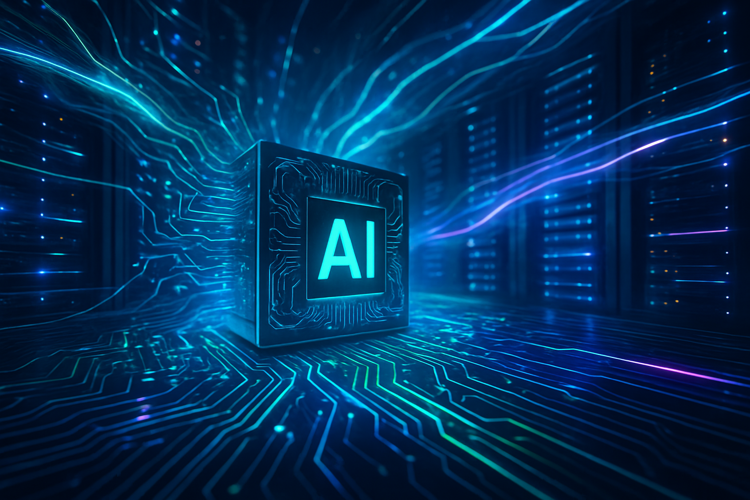
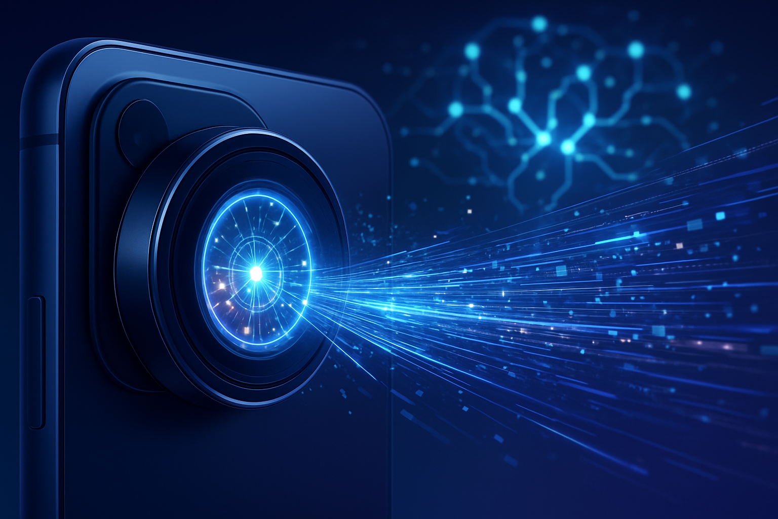
    Engineering Vision: The Semiconductor Heartbeat of AI Imaging

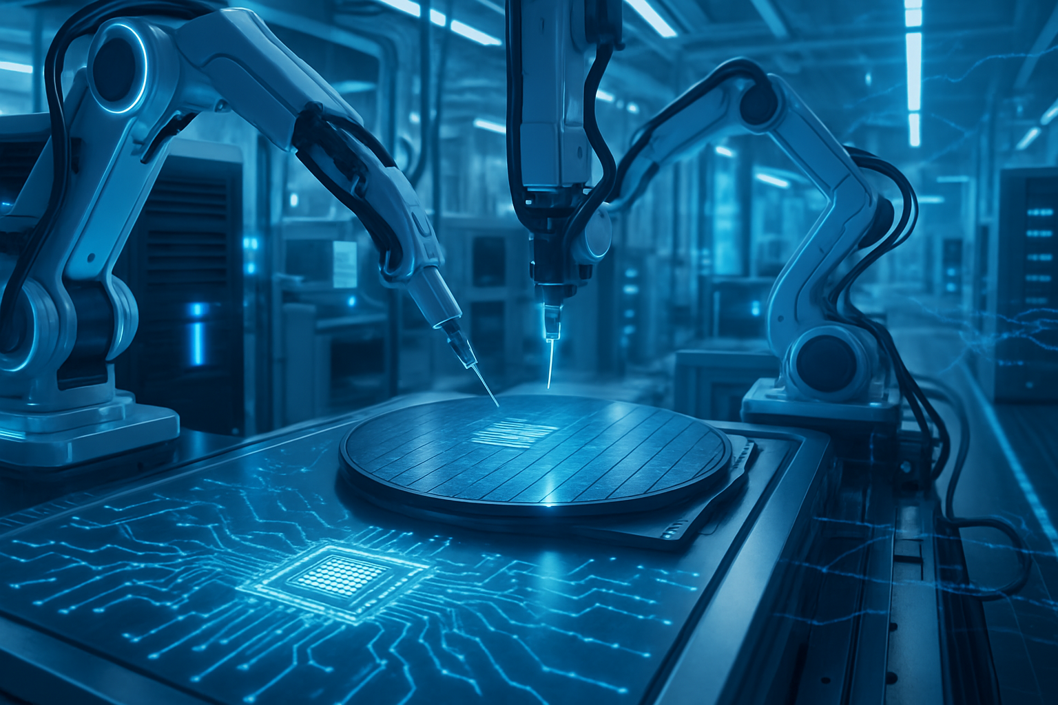
    The technological prowess enabling the iPhone 18's rumored camera system stems from a confluence of groundbreaking semiconductor innovations. At the forefront are advanced image sensors, exemplified by Sony's (NYSE:SONY) pioneering 2-Layer Transistor Pixel stacked CMOS sensor. This design ingeniously separates photodiodes and pixel transistors onto distinct substrate layers, effectively doubling the saturation signal level and dramatically widening dynamic range while significantly curbing noise. The result is superior image quality, particularly in challenging low-light or high-contrast scenarios, a critical improvement for AI algorithms that thrive on clean, detailed data. This marks a significant departure from conventional single-layer designs, offering a foundational hardware leap for computational photography.

    Looking further ahead, both Sony (NYSE:SONY) and Samsung (KRX:005930) are reportedly exploring even more ambitious multi-layered stacked sensor architectures, with whispers of a 3-layer stacked sensor (PD-TR-Logic) potentially destined for Apple's (NASDAQ:AAPL) future iPhones. These designs aim to reduce processing speeds by minimizing data travel distances, potentially unlocking resolutions nearing 500-600 megapixels. Complementing these advancements are Samsung's "Humanoid Sensors," which seek to integrate AI directly onto the image sensor, allowing for on-sensor data processing. This paradigm shift, also pursued by SK Hynix with its combined AI chip and image sensor units, enables faster processing, lower power consumption, and improved object recognition by processing data at the source, moving beyond traditional post-capture analysis.

    The evolution extends beyond mere pixel capture. Modern camera modules are increasingly integrating AI and machine learning capabilities directly into their Image Signal Processors (ISPs) and dedicated Neural Processing Units (NPUs). These on-device AI processors are the workhorses for real-time scene analysis, object detection, and sophisticated image enhancement, reducing reliance on cloud processing. Chipsets from MediaTek (TPE:2454) and Samsung's (KRX:005930) Exynos series, for instance, are designed with powerful integrated CPU, GPU, and NPU cores to handle complex AI tasks, enabling advanced computational photography techniques like multi-frame HDR, noise reduction, and super-resolution. This on-device processing capability is crucial for the iPhone 18, ensuring privacy, speed, and efficiency for its advanced AI imaging features.

    The initial reactions from the AI research community and industry experts have been overwhelmingly positive, emphasizing the transformative potential of these integrated hardware-software solutions. Experts foresee a future where the camera is not just a recording device but an intelligent interpreter of reality. The shift towards on-sensor AI and more powerful on-device NPUs is seen as critical for overcoming the physical limitations of mobile camera optics, allowing software and AI to drive the majority of image quality improvements and unlock entirely new photographic and augmented reality experiences.

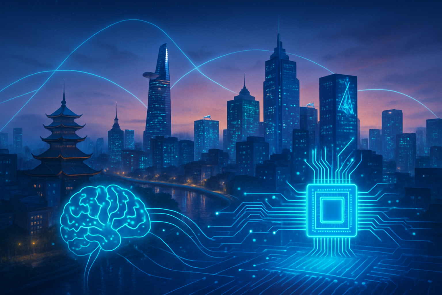
    Industry Tremors: Reshaping the AI and Tech Landscape

    The advent of next-generation mobile camera semiconductors, deeply integrated with AI capabilities, is poised to send ripples across the tech industry, profoundly impacting established giants and creating new avenues for nimble startups. Apple (NASDAQ:AAPL), with its vertically integrated approach, stands to further solidify its premium market position. By designing custom silicon with advanced neural engines, Apple can deliver highly optimized, secure, and personalized AI experiences, from cinematic-grade video to advanced photo editing, reinforcing its control over the entire user journey. The iPhone 18 will undoubtedly showcase this tight hardware-software synergy.

    Component suppliers like Sony (NYSE:SONY) and Samsung (KRX:005930) are locked in an intense race to innovate. Sony, the dominant image sensor supplier, is developing AI-enhanced sensors with on-board edge processing, such as the IMX500, minimizing the need for external processors and offering faster, more secure, and power-efficient solutions. However, Samsung's aggressive pursuit of "Humanoid Sensors" and its ambition to replicate human vision by 2027, potentially with 500-600 megapixel capabilities and "invisible" object detection, positions it as a formidable challenger, aiming to surpass Sony in the "On-Sensor AI" domain. For its own Galaxy devices, this translates to real-time optimization and advanced editing features powered by Galaxy AI, sharpening its competitive edge against Apple.

    Qualcomm (NASDAQ:QCOM) and MediaTek (TPE:2454), key providers of mobile SoCs, are embedding sophisticated AI capabilities into their platforms. Qualcomm's Snapdragon chips leverage Cognitive ISPs and powerful AI Engines for real-time semantic segmentation and contextual camera optimizations, maintaining its leadership in the Android ecosystem. MediaTek's Dimensity chipsets focus on power-efficient AI and imaging, supporting high-resolution cameras and generative AI features, strengthening its position, especially in high-end Android markets outside the US. Meanwhile, TSMC (NYSE:TSM), as the leading semiconductor foundry, remains an indispensable partner, providing the cutting-edge manufacturing processes essential for these complex, AI-centric components.

    This technological shift also creates fertile ground for AI startups. Companies specializing in ultra-efficient computer vision models, real-time 3D mapping, object tracking, and advanced image manipulation for edge devices can carve out niche markets or partner with larger tech firms. The competitive landscape is moving beyond raw hardware specifications to the sophistication of AI algorithms and seamless hardware-software integration. Vertical integration will offer a significant advantage, while component suppliers must continue to specialize, and the democratization of "professional" imaging capabilities could disrupt the market for entry-level dedicated cameras.

    Beyond the Lens: Wider Implications of AI Vision

    The integration of next-generation mobile camera semiconductors and AI-enhanced imaging extends far beyond individual devices, signifying a profound shift in the broader AI landscape and our interaction with technology. This advancement is a cornerstone of the broader "edge AI" trend, pushing sophisticated processing from the cloud directly onto devices. By enabling real-time scene recognition, advanced computational photography, and generative AI capabilities directly on a smartphone, devices like the iPhone 18 become intelligent visual interpreters, not just recorders. This aligns with the pervasive trend of making AI ubiquitous and deeply embedded in our daily lives, offering faster, more secure, and more responsive user experiences.

    The societal impacts are far-reaching. The democratization of professional-grade photography empowers billions, fostering new forms of digital storytelling and creative expression. AI-driven editing makes complex tasks intuitive, transforming smartphones into powerful creative companions. Furthermore, AI cameras are central to the evolution of Augmented Reality (AR) and Virtual Reality (VR), seamlessly blending digital content with the real world for applications in gaming, shopping, and education. Beyond personal use, these cameras are revolutionizing security through instant facial recognition and behavior analysis, and impacting healthcare with enhanced patient monitoring and diagnostics.

    However, these transformative capabilities come with significant concerns, most notably privacy. The widespread deployment of AI-powered cameras, especially with facial recognition, raises fears of pervasive mass surveillance and the potential for misuse of sensitive biometric data. The computational demands of running complex, real-time AI algorithms also pose challenges for battery life and thermal management, necessitating highly efficient NPUs and advanced cooling solutions. Moreover, the inherent biases in AI training data can lead to discriminatory outcomes, and the rise of generative AI tools for image manipulation (deepfakes) presents serious ethical dilemmas regarding misinformation and the authenticity of digital content.

    This era of AI-enhanced mobile camera technology represents a significant milestone, evolving from simpler "auto modes" to intelligent, context-aware scene understanding. It marks the "third wave" of smartphone camera innovation, moving beyond mere megapixels and lens size to computational photography that leverages software and powerful processors to overcome physical limitations. While making high-quality photography accessible to all, its nuanced impact on professional photography is still unfolding, even as mirrorless cameras also integrate AI. The shift to robust on-device AI, as seen in the iPhone 18's anticipated capabilities, is a key differentiator from earlier, cloud-dependent AI applications, marking a fundamental leap in intelligent visual processing.

    The Horizon of Vision: Future Trajectories of AI Imaging

    Looking ahead, the trajectory of AI-enhanced mobile camera technology, underpinned by cutting-edge semiconductors, promises an even more intelligent and immersive visual future for devices like the iPhone 18. In the near term (1-3 years), we can expect continuous refinement of existing computational photography, leading to unparalleled image quality across all conditions, smarter scene and object recognition, and more sophisticated real-time AI-generated enhancements for both photos and videos. AI-powered editing will become even more intuitive, with generative tools seamlessly modifying images and reconstructing backgrounds, as already demonstrated by current flagship devices. The focus will remain on robust on-device AI processing, leveraging dedicated NPUs to ensure privacy, speed, and efficiency.

    In the long term (3-5+ years), mobile cameras will evolve into truly intelligent visual assistants. This includes advanced 3D imaging and depth perception for highly realistic AR experiences, contextual recognition that allows cameras to interpret and act on visual information in real-time (e.g., identifying landmarks and providing historical context), and further integration of generative AI to create entirely new content from prompts or to suggest optimal framing. Video capabilities will reach new heights with intelligent tracking, stabilization, and real-time 4K HDR in challenging lighting. Experts predict that AI will become the bedrock of the mobile experience, with nearly all smartphones incorporating AI by 2025, transforming the camera into a "production partner" for content creation.

    The next generation of semiconductors will be the bedrock for these advancements. The iPhone 18 Pro, anticipated in 2026, is rumored to feature powerful new chips, potentially Apple's (NASDAQ:AAPL) M5, offering significant boosts in processing power and AI capabilities. Dedicated Neural Engines and NPUs will be crucial for handling complex machine learning tasks on-device, ensuring efficiency and security. Advanced sensor technology, such as rumored 200MP sensors from Samsung (KRX:005930) utilizing three-layer stacked CMOS image sensors with wafer-to-wafer hybrid bonding, will further enhance low-light performance and detail. Furthermore, features like variable aperture for the main camera and advanced packaging technologies like TSMC's (NYSE:TSM) CoWoS will improve integration and boost "Apple intelligence" capabilities, enabling a truly multimodal AI experience that processes and connects information across text, images, voice, and sensor data.

    Challenges remain, particularly concerning power consumption for complex AI algorithms, ensuring user privacy amidst vast data collection, mitigating biases in AI, and balancing automation with user customization. However, the potential applications are immense: from enhanced content creation for social media, interactive learning and shopping via AR, and personalized photography assistants, to advanced accessibility features and robust security monitoring. Experts widely agree that generative AI features will become so essential that future phones lacking this technology may feel archaic, fundamentally reshaping our expectations of mobile photography and visual interaction.

    A New Era of Vision: Concluding Thoughts on AI's Camera Revolution

    The advancements in next-generation mobile camera semiconductor technology, particularly as they converge to define devices like the iPhone 18, herald a new era in artificial intelligence. The key takeaway is a fundamental shift from cameras merely capturing light to actively understanding and intelligently interpreting the visual world. This profound integration of AI into the very hardware of mobile imaging systems is democratizing high-quality photography, making professional-grade results accessible to everyone, and transforming the smartphone into an unparalleled visual processing and creative tool.

    This development marks a significant milestone in AI history, pushing sophisticated machine learning to the "edge" of our devices. It underscores the increasing importance of computational photography, where software and dedicated AI hardware overcome the physical limitations of mobile optics, creating a seamless blend of art and algorithm. While offering immense benefits in creativity, accessibility, and new applications across various industries, it also demands careful consideration of ethical implications, particularly regarding privacy, data security, and the potential for AI bias and content manipulation.

    In the coming weeks and months, we should watch for further announcements from key players like Apple (NASDAQ:AAPL), Samsung (KRX:005930), and Sony (NYSE:SONY) regarding their next-generation chipsets and sensor technologies. The ongoing innovation in NPUs and on-sensor AI will be critical indicators of how quickly these advanced capabilities become mainstream. The evolving regulatory landscape around AI ethics and data privacy will also play a crucial role in shaping the deployment and public acceptance of these powerful new visual technologies. The future of mobile imaging is not just about clearer pictures; it's about smarter vision, fundamentally altering how we perceive and interact with our digital and physical realities.


    This content is intended for informational purposes only and represents analysis of current AI developments.

    TokenRing AI delivers enterprise-grade solutions for multi-agent AI workflow orchestration, AI-powered development tools, and seamless remote collaboration platforms.
    For more information, visit https://www.tokenring.ai/.

  • Oman’s Ambitious Silicon Dream: A New Regional Hub Poised to Revolutionize Global AI Hardware

    Oman’s Ambitious Silicon Dream: A New Regional Hub Poised to Revolutionize Global AI Hardware

    Oman is making a bold play to redefine its economic future, embarking on an ambitious initiative to establish itself as a regional semiconductor design hub. This strategic pivot, deeply embedded within the nation's Oman Vision 2040, aims to diversify its economy away from traditional oil revenues and propel it into the forefront of the global technology landscape. As of October 2025, significant strides have been made, positioning the Sultanate as a burgeoning center for cutting-edge AI chip design and advanced communication technologies.

    The immediate significance of Oman's endeavor extends far beyond its borders. By focusing on cultivating indigenous talent, attracting foreign investment, and fostering a robust ecosystem for semiconductor innovation, Oman is set to become a critical node in the increasingly complex global technology supply chain. This move is particularly crucial for the advancement of artificial intelligence, as the nation's emphasis on designing and manufacturing advanced AI chips promises to fuel the next generation of intelligent systems and applications worldwide.

    Laying the Foundation: Oman's Strategic Investments in AI Hardware

    Oman's initiative is built on a multi-pronged strategy, beginning with the recent launch of a National Innovation Centre. This center is envisioned as the nucleus of Oman's semiconductor ambitions, dedicated to cultivating local expertise in semiconductor design, wireless communication systems, and AI-powered networks. Collaborating with Omani universities, research institutes, and international technology firms, the center aims to establish a sustainable talent pipeline through advanced training programs. The emphasis on AI chip design is explicit, with the Ministry of Transport, Communications, and Information Technology (MoTCIT) highlighting that "AI would not be able to process massive volumes of data without semiconductors," underscoring the foundational role these chips will play.

    The Sultanate has also strategically forged key partnerships and attracted substantial investments. In February 2025, MoTCIT signed a Memorandum of Understanding (MoU) with EONH Private Holdings for an advanced chips and semiconductors project in the Salalah Free Zone, specifically targeting AI chip design and manufacturing. This was followed by a cooperation program in May 2025 with Indian technology firm Kinesis Semicon, aimed at establishing a large-scale integrated circuit (IC) design company and training 80 Omani engineers. Further bolstering its ecosystem, ITHCA Group, the technology investment arm of the Oman Investment Authority (OIA), invested in US-based Lumotive, leading to a partnership with GS Microelectronics (GSME) to create a LiDAR design and support center in Muscat. GSME had already opened Oman's first chip design office in 2022 and trained over 100 Omani engineers. Most recently, in October 2025, ITHCA Group invested $20 million in Movandi, a California-based developer of semiconductor and smart wireless solutions, which will see Movandi establish a regional R&D hub in Muscat focusing on smart communication and AI.

    This concentrated effort marks a significant departure from Oman's historical economic reliance on oil and gas. Instead of merely consuming technology, the nation is actively positioning itself as a creator and innovator in a highly specialized, capital-intensive sector. The focus on AI chips and advanced communication technologies demonstrates an understanding of future technological demands, aiming to produce high-value components critical for emerging AI applications like autonomous vehicles, sophisticated AI training systems, and 5G infrastructure. Initial reactions from industry observers and government officials within Oman are overwhelmingly positive, viewing these initiatives as crucial steps towards economic diversification and technological self-sufficiency, though the broader AI research community is still assessing the long-term implications of this emerging player.

    Reshaping the AI Industry Landscape

    Oman's emergence as a semiconductor design hub holds significant implications for AI companies, tech giants, and startups globally. Companies seeking to diversify their supply chains away from existing concentrated hubs in East Asia stand to benefit immensely from a new, strategically located design and potential manufacturing base. This initiative provides a new avenue for AI hardware procurement and collaboration, potentially mitigating geopolitical risks and increasing supply chain resilience, a lesson painfully learned during recent global disruptions.

    Major AI labs and tech companies, particularly those involved in developing advanced AI models and hardware (e.g., NVIDIA (NASDAQ: NVDA), Intel (NASDAQ: INTC), AMD (NASDAQ: AMD)), could find new partnership opportunities for R&D and specialized chip design services. While Oman's immediate focus is on design, the long-term vision includes manufacturing, which could eventually offer alternative fabrication options. Startups specializing in niche AI hardware, such as those focused on edge AI, IoT, or specific communication protocols, might find a more agile and supportive ecosystem in Oman for prototyping and initial production runs, especially given the explicit focus on cultivating local talent and fostering innovation.

    The competitive landscape could see subtle shifts. While Oman is unlikely to immediately challenge established giants, its focus on AI-specific chips and advanced communication solutions could create a specialized niche. This could lead to a healthy disruption in areas where innovation is paramount, potentially fostering new design methodologies and intellectual property. Companies like Movandi, which has already partnered with ITHCA Group, gain a strategic advantage by establishing an early foothold in this burgeoning regional hub, allowing them to tap into new talent pools and markets. For AI companies, this initiative represents an opportunity to collaborate with a nation actively investing in the foundational hardware that powers their innovations, potentially leading to more customized and efficient AI solutions.

    Oman's Role in the Broader AI Ecosystem

    Oman's semiconductor initiative fits squarely into the broader global trend of nations striving for technological sovereignty and economic diversification, particularly in critical sectors like semiconductors. It represents a significant step towards decentralizing the global chip design and manufacturing landscape, which has long been concentrated in a few key regions. This decentralization is vital for the resilience of the entire AI ecosystem, as a more distributed supply chain can better withstand localized disruptions, whether from natural disasters, geopolitical tensions, or pandemics.

    The impact on global AI development is profound. By fostering a new hub for AI chip design, Oman directly contributes to the accelerating pace of innovation in AI hardware. Advanced AI applications, from sophisticated large language models to complex autonomous systems, are heavily reliant on powerful, specialized semiconductors. Oman's focus on these next-generation chips will help meet the escalating demand, driving further breakthroughs in AI capabilities. Potential concerns, however, include the long-term sustainability of talent acquisition and retention in a highly competitive global market, as well as the immense capital investment required to scale from design to full-fledged manufacturing. The initiative will also need to navigate the complexities of international intellectual property laws and technology transfer.

    Comparisons to previous AI milestones underscore the significance of foundational hardware. Just as the advent of powerful GPUs revolutionized deep learning, the continuous evolution and diversification of AI-specific chip design hubs are crucial for the next wave of AI innovation. Oman's strategic investment is not just about economic diversification; it's about becoming a key enabler for the future of artificial intelligence, providing the very "brains" that power intelligent systems. This move aligns with a global recognition that hardware innovation is as critical as algorithmic advancements for AI's continued progress.

    The Horizon: Future Developments and Challenges

    In the near term, experts predict that Oman will continue to focus on strengthening its design capabilities and expanding its talent pool. The partnerships already established, particularly with firms like Movandi and Kinesis Semicon, are expected to yield tangible results in terms of new chip designs and trained engineers within the next 12-24 months. The National Innovation Centre will likely become a vibrant hub for R&D, attracting more international collaborations and fostering local startups in the semiconductor and AI hardware space. Long-term developments could see Oman moving beyond design to outsourced semiconductor assembly and test (OSAT) services, and eventually, potentially, even some specialized fabrication, leveraging projects like the polysilicon plant at Sohar Freezone.

    Potential applications and use cases on the horizon are vast, spanning across industries. Omani-designed AI chips could power advanced smart city initiatives across the Middle East, enable more efficient oil and gas exploration through AI analytics, or contribute to next-generation telecommunications infrastructure, including 5G and future 6G networks. Beyond these, the chips could find applications in automotive AI for autonomous driving systems, industrial automation, and even consumer electronics, particularly in edge AI devices that require powerful yet efficient processing.

    However, significant challenges need to be addressed. Sustaining the momentum of talent development and preventing brain drain will be crucial. Competing with established global semiconductor giants for both talent and market share will require continuous innovation, robust government support, and agile policy-making. Furthermore, attracting the massive capital investment required for advanced fabrication facilities remains a formidable hurdle. Experts predict that Oman's success will hinge on its ability to carve out specialized niches, leverage its strategic geographic location, and maintain strong international partnerships, rather than attempting to compete head-on with the largest players in all aspects of semiconductor manufacturing.

    Oman's AI Hardware Vision: A New Chapter Unfolds

    Oman's ambitious initiative to become a regional semiconductor design hub represents a pivotal moment in its economic transformation and a significant development for the global AI landscape. The key takeaways include a clear strategic shift towards a knowledge-based economy, substantial government and investment group backing, a strong focus on AI chip design, and a commitment to human capital development through partnerships and dedicated innovation centers. This move aims to enhance global supply chain resilience, foster innovation in AI hardware, and diversify the Sultanate's economy.

    The significance of this development in AI history cannot be overstated. It marks the emergence of a new, strategically important player in the foundational technology that powers artificial intelligence. By actively investing in the design and eventual manufacturing of advanced semiconductors, Oman is not merely participating in the tech revolution; it is striving to become an enabler and a driver of it. This initiative stands as a testament to the increasing recognition worldwide that control over critical hardware is paramount for national economic security and technological advancement.

    In the coming weeks and months, observers should watch for further announcements regarding new partnerships, the progress of the National Innovation Centre, and the first tangible outputs from the various design projects. The success of Oman's silicon dream will offer valuable lessons for other nations seeking to establish their foothold in the high-stakes world of advanced technology. Its journey will be a compelling narrative of ambition, strategic investment, and the relentless pursuit of innovation in the age of AI.


    This content is intended for informational purposes only and represents analysis of current AI developments.

    TokenRing AI delivers enterprise-grade solutions for multi-agent AI workflow orchestration, AI-powered development tools, and seamless remote collaboration platforms.
    For more information, visit https://www.tokenring.ai/.

  • AMD Unleashes AI Ambition: Strategic Partnerships and Next-Gen Instinct Accelerators Position Chipmaker as a Formidable NVIDIA Challenger

    AMD Unleashes AI Ambition: Strategic Partnerships and Next-Gen Instinct Accelerators Position Chipmaker as a Formidable NVIDIA Challenger

    Advanced Micro Devices' (NASDAQ: AMD) aggressive push into the AI hardware and software market has culminated in a series of groundbreaking announcements and strategic partnerships, fundamentally reshaping the competitive landscape of the semiconductor industry. With the unveiling of its MI300 series accelerators, the robust ROCm software ecosystem, and pivotal collaborations with industry titans like OpenAI and Oracle (NYSE: ORCL), Advanced Micro Devices (NASDAQ: AMD) is not merely participating in the AI revolution; it's actively driving a significant portion of it. These developments, particularly the multi-year, multi-generation agreement with OpenAI and the massive Oracle Cloud Infrastructure (OCI) deployment, signal a profound validation of AMD's comprehensive AI strategy and its potential to disrupt NVIDIA's (NASDAQ: NVDA) long-held dominance in AI compute.

    Detailed Technical Coverage

    The core of AMD's AI offensive lies in its Instinct MI300 series accelerators and the upcoming MI350 and MI450 generations. The AMD Instinct MI300X, launched in December 2023, stands out with its CDNA3 architecture, featuring an unprecedented 192 GB of HBM3 memory, 5.3 TB/s of peak memory bandwidth, and 153 billion transistors. This dense memory configuration is crucial for handling the massive parameter counts of modern generative AI models, offering leadership efficiency and performance. The accompanying AMD Instinct MI300X Platform integrates eight MI300X OAM devices, pooling 1.5 TB of HBM3 memory and achieving theoretical peak performance of 20.9 PFLOPs (FP8), providing a robust foundation for large-scale AI training and inference.

    Looking ahead, the AMD Instinct MI350 Series, based on the CDNA 4 architecture, is set to introduce support for new low-precision data types like FP4 and FP6, further enhancing efficiency for AI workloads. Oracle has already announced the general availability of OCI Compute with AMD Instinct MI355X GPUs, highlighting the immediate adoption of these next-gen accelerators. Beyond that, the AMD Instinct MI450 Series, slated for 2026, promises even greater capabilities with up to 432 GB of HBM4 memory and an astounding 20 TB/s of memory bandwidth, positioning AMD for significant future deployments with key partners like OpenAI and Oracle.

    AMD's approach significantly differs from traditional monolithic GPU designs by leveraging state-of-the-art die stacking and chiplet technology. This modular design allows for greater flexibility, higher yields, and improved power efficiency, crucial for the demanding requirements of AI and HPC. Furthermore, AMD's unwavering commitment to its open-source ROCm software stack directly challenges NVIDIA's proprietary CUDA ecosystem. The recent ROCm 7.0 Platform release significantly boosts AI inference performance (up to 3.5x over ROCm 6), expands compatibility to Windows and Radeon GPUs, and introduces full support for MI350 series and FP4/FP6 data types. This open strategy aims to foster broader developer adoption and mitigate vendor lock-in, a common pain point for hyperscalers.

    Initial reactions from the AI research community and industry experts have been largely positive, viewing AMD's advancements as a critical step towards diversifying the AI compute landscape. Analysts highlight the OpenAI partnership as a "major validation" of AMD's AI strategy, signaling that AMD is now a credible alternative to NVIDIA. The emphasis on open standards, coupled with competitive performance metrics, has garnered attention from major cloud providers and AI firms eager to reduce their reliance on a single supplier and optimize their total cost of ownership (TCO) for massive AI infrastructure deployments.

    Impact on AI Companies, Tech Giants, and Startups

    AMD's aggressive foray into the AI accelerator market, spearheaded by its Instinct MI300X and MI450 series GPUs and fortified by its open-source ROCm software stack, is sending ripples across the entire AI industry. Tech giants like Microsoft (NASDAQ: MSFT), Meta Platforms (NASDAQ: META), and Oracle (NYSE: ORCL) are poised to be major beneficiaries, gaining a crucial alternative to NVIDIA's (NASDAQ: NVDA) dominant AI hardware. Microsoft Azure already supports AMD ROCm software, integrating it to scale AI workloads, and plans to leverage future generations of Instinct accelerators. Meta is actively deploying MI300X for its Llama 405B models, and Oracle Cloud Infrastructure (OCI) is building a massive AI supercluster with 50,000 MI450 Series GPUs, marking a significant diversification of their AI compute infrastructure. This diversification reduces vendor lock-in, potentially leading to better pricing, more reliable supply chains, and greater flexibility in hardware choices for these hyperscalers.

    The competitive implications for major AI labs and tech companies are profound. For NVIDIA, AMD's strategic partnerships, particularly the multi-year, multi-generation agreement with OpenAI, represent the most direct and significant challenge to its near-monopoly in AI GPUs. While NVIDIA maintains a substantial lead with its mature CUDA ecosystem, AMD's Instinct series offers competitive performance, especially in memory-intensive workloads, often at a more attractive price point. OpenAI's decision to partner with AMD signifies a strategic effort to diversify its chip suppliers and directly influence AMD's hardware and software development, intensifying the competitive pressure on NVIDIA to innovate faster and potentially adjust its pricing strategies.

    This shift also brings potential disruption to existing products and services across the AI landscape. AMD's focus on an open ecosystem with ROCm and its deep software integration efforts (including making OpenAI's Triton language compatible with AMD chips) makes it easier for developers to utilize AMD hardware. This fosters innovation by providing viable alternatives to CUDA, potentially reducing costs and increasing access to high-performance compute. AI companies, especially those building large language models, can leverage AMD's memory-rich GPUs for larger models without extensive partitioning. Startups, often constrained by long waitlists and high costs for NVIDIA chips, can find a credible alternative hardware provider, lowering the barrier to entry for scalable AI infrastructure through AMD-powered cloud instances.

    Strategically, AMD is solidifying its market positioning as a strong contender and credible alternative to NVIDIA, moving beyond a mere "second-source" mentality. The Oracle deal alone is projected to bring substantial revenue and position AMD as a preferred partner for large-scale AI infrastructure. Analysts project significant growth in AMD's AI-related revenues, potentially reaching $20 billion by 2027. This strong positioning is built on a foundation of high-performance hardware, a robust and open software ecosystem, and critical strategic alliances that are reshaping how the industry views and procures AI compute.

    Wider Significance

    AMD's aggressive push into the AI sector, marked by its advanced Instinct GPUs and strategic alliances, fits squarely into the broader AI landscape's most critical trends: the insatiable demand for high-performance compute, the industry's desire for supply chain diversification, and the growing momentum for open-source ecosystems. The sheer scale of the deals, particularly the "6 gigawatt agreement" with OpenAI and Oracle's deployment of 50,000 MI450 Series GPUs, underscores the unprecedented demand for AI infrastructure. This signifies a crucial maturation of the AI market, where major players are actively seeking alternatives to ensure resilience and avoid vendor lock-in, a trend that will profoundly impact the future trajectory of AI development.

    The impacts of AMD's strategy are multifaceted. Increased competition in the AI hardware market will undoubtedly accelerate innovation, potentially leading to more advanced hardware, improved software tools, and better price-performance ratios for customers. This diversification of AI compute power is vital for mitigating risks associated with reliance on a single vendor and ensures greater flexibility in sourcing essential compute. Furthermore, AMD's steadfast commitment to its open-source ROCm platform directly challenges NVIDIA's proprietary CUDA, fostering a more collaborative and open AI development community. This open approach, akin to the rise of Linux against proprietary operating systems, could democratize access to high-performance AI compute, driving novel approaches and optimizations across the industry. The high memory capacity of AMD's GPUs also influences AI model design, allowing larger models to fit onto a single GPU, simplifying development and deployment.

    However, potential concerns temper this optimistic outlook. Supply chain challenges, particularly U.S. export controls on advanced AI chips and reliance on TSMC for manufacturing, pose revenue risks and potential bottlenecks. While AMD is exploring mitigation strategies, these remain critical considerations. The maturity of the ROCm software ecosystem, while rapidly improving, still lags behind NVIDIA's CUDA in terms of overall breadth of optimized libraries and community support. Developers migrating from CUDA may face a learning curve or encounter varying performance. Nevertheless, AMD's continuous investment in ROCm and strategic partnerships are actively bridging this gap. The immense scale of AI infrastructure deals also raises questions about financing and the development of necessary power infrastructure, which could pose risks if economic conditions shift.

    Comparing AMD's current AI strategy to previous AI milestones reveals a similar pattern of technological competition and platform shifts. NVIDIA's CUDA established a proprietary advantage, much like Microsoft's Windows in the PC era. AMD's embrace of open-source ROCm is a direct challenge to this, aiming to prevent a single vendor from completely dictating the future of AI. This "AI supercycle," as AMD CEO Lisa Su describes it, is akin to other major technological disruptions, where massive investments drive rapid innovation and reshape industries. AMD's emergence as a viable alternative at scale marks a crucial inflection point, moving towards a more diversified and competitive landscape, which historically has spurred greater innovation and efficiency across the tech world.

    Future Developments

    AMD's trajectory in the AI market is defined by an aggressive and clearly articulated roadmap, promising continuous innovation in both hardware and software. In the near term (1-3 years), the company is committed to an annual release cadence for its Instinct accelerators. The Instinct MI325X, with 288GB of HBM3E memory, is expected to see widespread system availability in Q1 2025. Following this, the Instinct MI350 Series, based on the CDNA 4 architecture and built on TSMC’s 3nm process, is slated for 2025, introducing support for FP4 and FP6 data types. Oracle Cloud Infrastructure (NYSE: ORCL) is already deploying MI355X GPUs at scale, signaling immediate adoption. Concurrently, the ROCm software stack will see continuous optimization and expansion, ensuring compatibility with a broader array of AI frameworks and applications. AMD's "Helios" rack-scale solution, integrating GPUs, future EPYC CPUs, and Pensando networking, is also expected to move from reference design to volume deployment by 2026.

    Looking further ahead (3+ years), AMD's long-term vision includes the Instinct MI400 Series in 2026, featuring the CDNA-Next architecture and projecting 432GB of HBM4 memory with 20TB/s bandwidth. This generation is central to the massive deployments planned with Oracle (50,000 MI450 chips starting Q3 2026) and OpenAI (1 gigawatt of MI450 computing power by H2 2026). Beyond that, the Instinct MI500X Series and EPYC "Verano" CPUs are planned for 2027, potentially leveraging TSMC's A16 (1.6 nm) process. These advancements will power a vast array of applications, from hyperscale AI model training and inference in data centers and cloud environments to high-performance, low-latency AI inference at the edge for autonomous vehicles, industrial automation, and healthcare. AMD is also expanding its AI PC portfolio with Ryzen AI processors, bringing advanced AI capabilities directly to consumer and business devices.

    Despite this ambitious roadmap, significant challenges remain. NVIDIA's (NASDAQ: NVDA) entrenched dominance and its mature CUDA software ecosystem continue to be AMD's primary hurdle; while ROCm is rapidly evolving, sustained effort is needed to bridge the gap in developer adoption and library support. AMD also faces critical supply chain risks, particularly in scaling production of its advanced chips and navigating geopolitical export controls. Pricing pressure from intensifying competition and the immense energy demands of scaling AI infrastructure are additional concerns. However, experts are largely optimistic, predicting substantial market share gains (up to 30% in next-gen data center infrastructure) and significant revenue growth for AMD's AI segment, potentially reaching $20 billion by 2027. The consensus is that while execution is key, AMD's open ecosystem strategy and competitive hardware position it as a formidable contender in the evolving AI landscape.

    Comprehensive Wrap-up

    Advanced Micro Devices (NASDAQ: AMD) has undeniably emerged as a formidable force in the AI market, transitioning from a challenger to a credible co-leader in the rapidly evolving landscape of AI computing. The key takeaways from its recent strategic maneuvers are clear: a potent combination of high-performance Instinct MI series GPUs, a steadfast commitment to the open-source ROCm software ecosystem, and transformative partnerships with AI behemoths like OpenAI and Oracle (NYSE: ORCL) are fundamentally reshaping the competitive dynamics. AMD's superior memory capacity in its MI300X and future GPUs, coupled with an attractive total cost of ownership (TCO) and an open software model, positions it for substantial market share gains, particularly in the burgeoning inference segment of AI workloads.

    These developments mark a significant inflection point in AI history, introducing much-needed competition into a market largely dominated by NVIDIA (NASDAQ: NVDA). OpenAI's decision to partner with AMD, alongside Oracle's massive GPU deployment, serves as a profound validation of AMD's hardware and, crucially, its ROCm software platform. This establishes AMD as an "essential second source" for high-performance GPUs, mitigating vendor lock-in and fostering a more diversified, resilient, and potentially more innovative AI infrastructure landscape. The long-term impact points towards a future where AI development is less constrained by proprietary ecosystems, encouraging broader participation and accelerating the pace of innovation across the industry.

    Looking ahead, investors and industry observers should closely monitor several key areas. Continued investment and progress in the ROCm ecosystem will be paramount to further close the feature and maturity gap with CUDA and drive broader developer adoption. The successful rollout and deployment of the next-generation MI350 series (expected mid-2025) and MI400 series (2026) will be critical to sustaining AMD's competitive edge and meeting the escalating demand for advanced AI workloads. Keep an eye out for additional partnership announcements with other major AI labs and cloud providers, leveraging the substantial validation provided by the OpenAI and Oracle deals. Tracking AMD's actual market share gains in the AI GPU segment and observing NVIDIA's competitive response, particularly regarding its pricing strategies and upcoming hardware, will offer further insights into the unfolding AI supercycle. Finally, AMD's quarterly earnings reports, especially data center segment revenue and updated guidance for AI chip sales, will provide tangible evidence of the impact of these strategic moves in the coming weeks and months.


    This content is intended for informational purposes only and represents analysis of current AI developments.

    TokenRing AI delivers enterprise-grade solutions for multi-agent AI workflow orchestration, AI-powered development tools, and seamless remote collaboration platforms.
    For more information, visit https://www.tokenring.ai/.

  • Ho Chi Minh City Ignites Southeast Asia’s AI and Semiconductor Revolution: A Bold Vision for a High-Tech Future

    Ho Chi Minh City Ignites Southeast Asia’s AI and Semiconductor Revolution: A Bold Vision for a High-Tech Future

    Ho Chi Minh City (HCMC) is embarking on an ambitious journey to transform itself into a powerhouse for Artificial Intelligence (AI) and semiconductor development, a strategic pivot poised to reshape the technological landscape of Southeast Asia. This bold initiative, backed by substantial government investment and critical international partnerships, signifies Vietnam's intent to move beyond manufacturing and into high-value innovation. The city's comprehensive strategy focuses intensely on cultivating a highly skilled engineering workforce and fostering a robust research and development (R&D) ecosystem, setting the stage for a new era of technological leadership in the region.

    This strategic bet is not merely aspirational; it is a meticulously planned blueprint with concrete targets extending to 2045. As of October 9, 2025, HCMC is actively implementing programs designed to attract top-tier talent, establish world-class R&D centers, and integrate its burgeoning tech sector into global supply chains. The immediate significance lies in the potential for HCMC to become a crucial node in the global semiconductor and AI industries, offering an alternative and complementary hub to existing centers, while simultaneously driving significant economic growth and technological advancement within Vietnam.

    Unpacking HCMC's High-Tech Blueprint: From Talent Nurturing to R&D Apex

    HCMC's strategic blueprint is characterized by a multi-pronged approach to cultivate a thriving AI and semiconductor ecosystem. At its core is an aggressive talent development program, aiming to train at least 9,000 university-level engineers for the semiconductor industry by 2030. This encompasses not only integrated circuit (IC) design but also crucial adjacent fields such as AI, big data, cybersecurity, and blockchain. Nationally, Vietnam envisions training 50,000 semiconductor engineers by 2030, and an impressive 100,000 engineers across AI and semiconductor fields in the coming years, underscoring the scale of this human capital investment.

    To achieve these ambitious targets, HCMC is investing heavily in specialized training programs. The Saigon Hi-Tech Park (SHTP) Training Center is being upgraded to an internationally standardized facility, equipped with advanced laboratories, workshops, and computer rooms. This hands-on approach is complemented by robust university-industry collaborations, with local universities and colleges expanding their semiconductor-related curricula. Furthermore, global tech giants are directly involved: Advanced Micro Devices, Inc. (NASDAQ: AMD) is coordinating intensive training courses in AI, microchip design, and semiconductor technology, while Intel Corporation (NASDAQ: INTC) is partnering with HCMC to launch an AI workforce training program targeting public officials and early-career professionals.

    Beyond talent, HCMC is committed to fostering a vibrant R&D environment. The city plans to establish at least one international-standard R&D center by 2030 and aims for at least five internationally recognized Centers of Excellence (CoE) in critical technology fields. The SHTP is prioritizing the completion of R&D infrastructure for semiconductor chips, specifically focusing on packaging and testing facilities. A national-level shared semiconductor laboratory at Vietnam National University – HCMC is also underway, poised to enhance research capacity and accelerate product testing. By 2030, HCMC aims to allocate 2% of its Gross Regional Domestic Product (GRDP) to R&D, a significant increase that highlights its dedication to innovation.

    This concerted effort distinguishes HCMC's strategy from mere industrial expansion. It's a holistic ecosystem play, integrating education, research, and industry to create a self-sustaining innovation hub. Initial reactions from the AI research community and industry experts have been largely positive, recognizing Vietnam's strong potential due to its large, young, and increasingly educated workforce, coupled with proactive government policies. The emphasis on both AI and semiconductors also reflects a forward-thinking approach, acknowledging the intertwined nature of these two critical technologies in driving future innovation.

    Reshaping the Competitive Landscape: Opportunities and Disruptions

    Ho Chi Minh City's aggressive push into AI and semiconductor development stands to significantly impact a wide array of AI companies, tech giants, and startups globally. Companies with existing manufacturing or R&D footprints in Vietnam, such as Intel Corporation (NASDAQ: INTC), which already operates one of its largest global assembly and test facilities in HCMC and recently began producing its advanced 18A chip technology there, are poised to benefit immensely. This strategic alignment could lead to further expansion and deeper integration into the Vietnamese innovation ecosystem, leveraging local talent and government incentives.

    Beyond existing players, this development creates fertile ground for new investments and partnerships. Advanced Micro Devices, Inc. (NASDAQ: AMD) has already signed a Memorandum of Understanding (MoU) with HCMC, exploring the establishment of an R&D Centre and supporting policy development. NVIDIA Corporation (NASDAQ: NVDA) is also actively collaborating with the Vietnamese government, signing an AI cooperation agreement to establish an AI research and development center and an AI data center, even exploring shifting part of its manufacturing to Vietnam. These collaborations underscore HCMC's growing appeal as a strategic location for high-tech operations, offering proximity to talent and a supportive regulatory environment.

    For smaller AI labs and startups, HCMC presents a compelling new frontier. The availability of a rapidly growing pool of skilled engineers, coupled with dedicated R&D infrastructure and government incentives, could lower operational costs and accelerate innovation. This might lead to a decentralization of AI development, with more startups choosing HCMC as a base, potentially disrupting the dominance of established tech hubs. The focus on generative and agentic AI, as evidenced by Qualcomm Incorporated's (NASDAQ: QCOM) new AI R&D center in Vietnam, indicates a commitment to cutting-edge research that could attract specialized talent and foster groundbreaking applications.

    The competitive implications extend to global supply chains. As HCMC strengthens its position in semiconductor design, packaging, and testing, it could offer a more diversified and resilient alternative to existing manufacturing centers, reducing geopolitical risks for tech giants. For companies heavily reliant on AI hardware and software development, HCMC's emergence could mean access to new talent pools, innovative R&D capabilities, and a more competitive landscape for sourcing technology solutions, ultimately driving down costs and accelerating product cycles.

    Broader Significance: A New Dawn for Southeast Asian Tech

    Ho Chi Minh City's strategic foray into AI and semiconductor development represents a pivotal moment in the broader AI landscape, signaling a significant shift in global technological power. This initiative aligns perfectly with the overarching trend of decentralization in tech innovation, moving beyond traditional hubs in Silicon Valley, Europe, and East Asia. It underscores a growing recognition that diverse talent pools and supportive government policies in emerging economies can foster world-class technological ecosystems.

    The impacts of this strategy are multifaceted. Economically, it promises to elevate Vietnam's position in the global value chain, transitioning from a manufacturing-centric economy to one driven by high-tech R&D and intellectual property. Socially, it will create high-skilled jobs, foster a culture of innovation, and potentially improve living standards through technological advancement. Environmentally, the focus on digital and green transformation, with investments like the VND125 billion (approximately US$4.9 million) Digital and Green Transformation Research Center at SHTP, suggests a commitment to sustainable technological growth, a crucial consideration in the face of global climate challenges.

    Potential concerns, however, include the significant investment required to sustain this growth, the challenge of rapidly scaling a high-quality engineering workforce, and the need to maintain intellectual property protections in a competitive global environment. The success of HCMC's vision will depend on consistent policy implementation, continued international collaboration, and the ability to adapt to the fast-evolving technological landscape. Nevertheless, comparisons to previous AI milestones and breakthroughs highlight HCMC's proactive approach. Much like how countries like South Korea and Taiwan strategically invested in semiconductors decades ago to become global leaders, HCMC is making a similar long-term bet on the foundational technologies of the 21st century.

    This move also has profound geopolitical implications, potentially strengthening Vietnam's strategic importance as a reliable partner in the global tech supply chain. As nations increasingly seek to diversify their technological dependencies, HCMC's emergence as an AI and semiconductor hub offers a compelling alternative, fostering greater resilience and balance in the global technology ecosystem. It's a testament to the idea that innovation can flourish anywhere with the right vision, investment, and human capital.

    The Road Ahead: Anticipating Future Milestones and Challenges

    Looking ahead, the near-term developments for Ho Chi Minh City's AI and semiconductor ambitions will likely focus on the accelerated establishment of the planned R&D centers and Centers of Excellence, particularly within the Saigon Hi-Tech Park. We can expect to see a rapid expansion of specialized training programs in universities and technical colleges, alongside the rollout of initial cohorts of semiconductor and AI engineers. The operationalization of the national-level shared semiconductor laboratory at Vietnam National University – HCMC will be a critical milestone, enabling advanced research and product testing. Furthermore, more announcements regarding foreign direct investment and partnerships from global tech companies, drawn by the burgeoning ecosystem and attractive incentives, are highly probable in the coming months.

    In the long term, the potential applications and use cases stemming from HCMC's strategic bet are vast. A robust local AI and semiconductor industry could fuel innovation in smart cities, advanced manufacturing, healthcare, and autonomous systems. The development of indigenous AI solutions and chip designs could lead to new products and services tailored for the Southeast Asian market and beyond. Experts predict that HCMC could become a key player in niche areas of semiconductor manufacturing, such as advanced packaging and testing, and a significant hub for AI model development and deployment, especially in areas requiring high-performance computing.

    However, several challenges need to be addressed. Sustaining the momentum of talent development will require continuous investment in education and a dynamic curriculum that keeps pace with technological advancements. Attracting and retaining top-tier international researchers and engineers will be crucial for accelerating R&D capabilities. Furthermore, navigating the complex global intellectual property landscape and ensuring robust cybersecurity measures will be paramount to protecting innovations and fostering trust. Experts predict that while HCMC has laid a strong foundation, its success will ultimately hinge on its ability to foster a truly innovative culture that encourages risk-taking, collaboration, and continuous learning, while maintaining a competitive edge against established global players.

    HCMC's Bold Leap: A Comprehensive Wrap-up

    Ho Chi Minh City's strategic push to become a hub for AI and semiconductor development represents one of the most significant technological initiatives in Southeast Asia in recent memory. The key takeaways include a clear, long-term vision extending to 2045, aggressive targets for training a highly skilled workforce, substantial investment in R&D infrastructure, and a proactive approach to forging international partnerships with industry leaders like Intel (NASDAQ: INTC), AMD (NASDAQ: AMD), NVIDIA (NASDAQ: NVDA), and Qualcomm (NASDAQ: QCOM). These efforts are designed to transform HCMC into a high-value innovation economy, moving beyond traditional manufacturing.

    This development holds immense significance in AI history, showcasing how emerging economies are strategically positioning themselves to become integral to the future of technology. It highlights a global shift towards a more diversified and resilient tech ecosystem, where talent and innovation are increasingly distributed across continents. HCMC's commitment to both AI and semiconductors underscores a profound understanding of the symbiotic relationship between these two critical fields, recognizing that advancements in one often drive breakthroughs in the other.

    The long-term impact could see HCMC emerge as a vital node in the global tech supply chain, a source of cutting-edge AI research, and a regional leader in high-tech manufacturing. It promises to create a ripple effect, inspiring other cities and nations in Southeast Asia to invest similarly in future-forward technologies. In the coming weeks and months, it will be crucial to watch for further announcements regarding government funding allocations, new university programs, additional foreign direct investments, and the progress of key infrastructure projects like the national-level shared semiconductor laboratory. HCMC's journey is not just a local endeavor; it's a testament to the power of strategic vision in shaping the global technological future.

    This content is intended for informational purposes only and represents analysis of current AI developments.
    TokenRing AI delivers enterprise-grade solutions for multi-agent AI workflow orchestration, AI-powered development tools, and seamless remote collaboration platforms.
    For more information, visit https://www.tokenring.ai/.

  • India’s Silicon Ascent: Maharashtra Eyes Chip Capital Crown by 2030, Fueling AI Ambitions

    India’s Silicon Ascent: Maharashtra Eyes Chip Capital Crown by 2030, Fueling AI Ambitions

    India is rapidly accelerating its ambitions in the global semiconductor landscape, with the state of Maharashtra spearheading a monumental drive to emerge as the nation's chip capital by 2030. This strategic push is not merely about manufacturing; it's intricately woven into India's broader Artificial Intelligence (AI) strategy, aiming to cultivate a robust indigenous ecosystem for chip design, fabrication, and packaging, thereby powering the next generation of AI innovations and ensuring technological sovereignty.

    At the heart of this talent cultivation lies the NaMo Semiconductor Lab, an initiative designed to sculpt future chip designers and engineers. These concerted efforts represent a pivotal moment for India, positioning it as a significant player in the high-stakes world of advanced electronics and AI, moving beyond being just a consumer to a formidable producer of critical technological infrastructure.

    Engineering India's AI Future: From Design to Fabrication

    India's journey towards semiconductor self-reliance is underpinned by the India Semiconductor Mission (ISM), launched in December 2021 with a substantial outlay of approximately $9.2 billion (₹76,000 crore). This mission provides a robust policy framework and financial incentives to attract both domestic and international investments into semiconductor and display manufacturing. As of August 2025, ten projects have already been approved, committing a cumulative investment of about $18.23 billion (₹1.60 trillion), signaling a strong trajectory towards establishing India as a reliable alternative hub in global technology supply chains. India anticipates its first domestically produced semiconductor chip to hit the market by the close of 2025, a testament to the accelerated pace of these initiatives.

    Maharashtra, in particular, has carved out its own pioneering semiconductor policy, actively fostering an ecosystem conducive to chip manufacturing. Key developments include the inauguration of RRP Electronics Ltd.'s first semiconductor manufacturing OSAT (Outsourced Semiconductor Assembly and Test) facility in Navi Mumbai in September 2024, backed by an investment of ₹12,035 crore, with plans for a FAB Manufacturing unit in its second phase. Furthermore, the Maharashtra cabinet has greenlit a significant $10 billion (₹83,947 crore) investment proposal for a semiconductor chip manufacturing unit by a joint venture between Tower Semiconductor and the Adani Group (NSE: ADANIENT) in Taloja, Navi Mumbai, targeting an initial capacity of 40,000 wafer starts per month (WSPM). The Vedanta Group (NSE: VEDL), in partnership with Foxconn (TWSE: 2317), has also proposed a massive ₹1.6 trillion (approximately $20.8 billion) investment for a semiconductor and display fabs manufacturing unit in Maharashtra. These initiatives are designed to reduce India's reliance on foreign imports and foster a "Chip to Ship" philosophy, emphasizing indigenous manufacturing from design to the final product.

    The NaMo Semiconductor Laboratory, approved at IIT Bhubaneswar and funded under the MPLAD Scheme with an estimated cost of ₹4.95 crore, is a critical component in developing the necessary human capital. This lab aims to equip Indian youth with industry-ready skills in chip manufacturing, design, and packaging, positioning IIT Bhubaneswar as a hub for semiconductor research and skilling. India already boasts 20% of the global chip design talent, with a vibrant academic ecosystem where students from 295 universities utilize advanced Electronic Design Automation (EDA) tools. The NaMo Lab will further enhance these capabilities, complementing existing facilities like the Silicon Carbide Research and Innovation Centre (SiCRIC) at IIT Bhubaneswar, and directly supporting the "Make in India" and "Design in India" initiatives.

    Reshaping the AI Industry Landscape

    India's burgeoning semiconductor sector is poised to significantly impact AI companies, both domestically and globally. By fostering indigenous chip design and manufacturing, India aims to create a more resilient supply chain, reducing the vulnerability of its AI ecosystem to geopolitical fluctuations and foreign dependencies. This localized production will directly benefit Indian AI startups and tech giants by providing easier access to specialized AI hardware, potentially at lower costs, and with greater customization options tailored to local needs.

    For major AI labs and tech companies, particularly those with a significant presence in India, this development presents both opportunities and competitive implications. Companies like Tata Electronics, which has already announced plans for semiconductor manufacturing, stand to gain strategic advantages. The availability of locally manufactured advanced chips, including those optimized for AI workloads, could accelerate innovation in areas such as machine learning, large language models, and edge AI applications. This could lead to a surge in AI-powered products and services developed within India, potentially disrupting existing markets and creating new ones.

    Furthermore, the "Design Linked Incentive (DLI)" scheme, which has already approved 23 chip-design projects led by local startups and MSMEs, is fostering a new wave of indigenous AI hardware development. Chips designed for surveillance cameras, energy meters, and IoT devices will directly feed into India's smart city and smart mobility initiatives, which are central to its AI for All vision. This localized hardware development could give Indian companies a unique competitive edge in developing AI solutions specifically suited for the diverse Indian market, and potentially for other emerging economies. The strategic advantage lies not just in manufacturing, but in owning the entire value chain from design to deployment, fostering a robust and self-reliant AI ecosystem.

    A Cornerstone of India's "AI for All" Vision

    India's semiconductor drive is intrinsically linked to its ambitious "AI for All" vision, positioning AI as a catalyst for inclusive growth and societal transformation. The national strategy, initially articulated by NITI Aayog in 2018 and further solidified by the IndiaAI Mission launched in 2024 with an allocation of ₹10,300 crore over five years, aims to establish India as a global leader in AI. Advanced chips are the fundamental building blocks for powering AI technologies, from data centers running large language models to edge devices enabling real-time AI applications. Without a robust and reliable supply of these chips, India's AI ambitions would be severely hampered.

    The impact extends far beyond economic growth. This initiative is a critical component of building a resilient AI infrastructure. The IndiaAI Mission focuses on developing a high-end common computing facility equipped with 18,693 Graphics Processing Units (GPUs), making it one of the most extensive AI compute infrastructures globally. The government has also approved ₹107.3 billion ($1.24 billion) in 2024 for AI-specific data center infrastructure, with investments expected to exceed $100 billion by 2027. This infrastructure, powered by increasingly indigenous semiconductors, will be vital for training and deploying complex AI models, ensuring that India has the computational backbone necessary to compete on the global AI stage.

    Potential concerns, however, include the significant capital investment required, the steep learning curve for advanced manufacturing processes, and the global competition for talent and resources. While India boasts a large pool of engineering talent, scaling up to meet the specialized demands of semiconductor manufacturing and advanced AI chip design requires continuous investment in education and training. Comparisons to previous AI milestones highlight that access to powerful, efficient computing hardware has always been a bottleneck. By proactively addressing this through a national semiconductor strategy, India is laying a crucial foundation that could prevent future compute-related limitations from impeding its AI progress.

    The Horizon: From Indigenous Chips to Global AI Leadership

    The near-term future promises significant milestones for India's semiconductor and AI sectors. The expectation of India's first domestically produced semiconductor chip reaching the market by the end of 2025 is a tangible marker of progress. The broader goal is for India to be among the top five semiconductor manufacturing nations by 2029, establishing itself as a reliable alternative hub for global technology supply chains. This trajectory indicates a rapid scaling up of production capabilities and a deepening of expertise across the semiconductor value chain.

    Looking further ahead, the potential applications and use cases are vast. Indigenous semiconductor capabilities will enable the development of highly specialized AI chips for various sectors, including defense, healthcare, agriculture, and smart infrastructure. This could lead to breakthroughs in areas such as personalized medicine, precision agriculture, autonomous systems, and advanced surveillance, all powered by chips designed and manufactured within India. Challenges that need to be addressed include attracting and retaining top-tier global talent, securing access to critical raw materials, and navigating the complex geopolitical landscape that often influences semiconductor trade and technology transfer. Experts predict that India's strategic investments will not only foster economic growth but also enhance national security and technological sovereignty, making it a formidable player in the global AI race.

    The integration of AI into diverse sectors, from smart cities to smart mobility, will be accelerated by the availability of locally produced, AI-optimized hardware. This synergy between semiconductor prowess and AI innovation is expected to contribute approximately $400 billion to the national economy by 2030, transforming India into a powerhouse of digital innovation and a leader in responsible AI development.

    A New Era of Self-Reliance in AI

    India's aggressive push into the semiconductor sector, exemplified by Maharashtra's ambitious goal to become the country's chip capital by 2030 and the foundational work of the NaMo Semiconductor Lab, marks a transformative period for the nation's technological landscape. This concerted effort is more than an industrial policy; it's a strategic imperative directly fueling India's broader AI strategy, aiming for self-reliance and global leadership in a domain critical to future economic growth and societal progress. The synergy between fostering indigenous chip design and manufacturing and cultivating a skilled AI workforce is creating a virtuous cycle, where advanced hardware enables sophisticated AI applications, which in turn drives demand for more powerful and specialized chips.

    The significance of this development in AI history cannot be overstated. By investing heavily in the foundational technology that powers AI, India is securing its place at the forefront of the global AI revolution. This proactive stance distinguishes India from many nations that primarily focus on AI software and applications, often relying on external hardware. The long-term impact will be a more resilient, innovative, and sovereign AI ecosystem capable of addressing unique national challenges and contributing significantly to global technological advancements.

    In the coming weeks and months, the world will be watching for further announcements regarding new fabrication plants, partnerships, and the first indigenous chips rolling off production lines. The success of Maharashtra's blueprint and the output of institutions like the NaMo Semiconductor Lab will be key indicators of India's trajectory. This is not just about building chips; it's about building the future of AI, Made in India, for India and the world.

    This content is intended for informational purposes only and represents analysis of current AI developments.

    TokenRing AI delivers enterprise-grade solutions for multi-agent AI workflow orchestration, AI-powered development tools, and seamless remote collaboration platforms.
    For more information, visit https://www.tokenring.ai/.

  • Amkor Technology’s $7 Billion Arizona Investment Ignites U.S. Semiconductor Manufacturing Renaissance

    Amkor Technology’s $7 Billion Arizona Investment Ignites U.S. Semiconductor Manufacturing Renaissance

    Peoria, Arizona – October 6, 2025 – In a landmark announcement poised to reshape the global semiconductor landscape, Amkor Technology (NASDAQ: AMKR) today officially broke ground on its expanded, state-of-the-art advanced packaging and test campus in Peoria, Arizona. This monumental $7 billion investment, significantly up from initial projections, marks a pivotal moment for U.S. manufacturing, establishing the nation's first high-volume advanced packaging facility. The move is a critical stride towards fortifying domestic supply chain resilience and cementing America's technological sovereignty in an increasingly competitive global arena.

    The immediate significance of Amkor's Arizona campus cannot be overstated. By bringing advanced packaging – a crucial, intricate step in chip manufacturing – back to U.S. soil, the project addresses a long-standing vulnerability in the domestic semiconductor ecosystem. It promises to create up to 3,000 high-quality jobs and serves as a vital anchor for the burgeoning semiconductor cluster in Arizona, further solidifying the state's position as a national hub for cutting-edge chip production.

    A Strategic Pivot: Onshoring Advanced Packaging for the AI Era

    Amkor Technology's $7 billion commitment in Peoria represents a profound strategic shift from its historical operating model. For decades, Amkor, a global leader in outsourced semiconductor assembly and test (OSAT) services, has relied on a globally diversified manufacturing footprint, primarily concentrated in East Asia. This new investment, however, signals a deliberate and aggressive pivot towards onshoring critical back-end processes, driven by national security imperatives and the relentless demand for advanced chips.

    The Arizona campus, spanning 104 acres within the Peoria Innovation Core, is designed to feature over 750,000 square feet of cleanroom space upon completion of both phases. It will specialize in advanced packaging and test technologies, including sophisticated 2.5D and 3D interposer solutions, essential for powering next-generation applications in artificial intelligence (AI), high-performance computing (HPC), mobile communications, and the automotive sector. This capability is crucial, as performance gains in modern chips increasingly depend on packaging innovations rather than just transistor scaling. The facility is strategically co-located to complement Taiwan Semiconductor Manufacturing Company's (TSMC) (NYSE: TSM) nearby wafer fabrication plants in Phoenix, enabling a seamless, integrated "start-to-finish" chip production process within Arizona. This proximity will significantly reduce lead times and enhance collaboration, circumventing the need to ship wafers overseas for crucial back-end processing.

    The project is substantially bolstered by the U.S. government's CHIPS and Science Act, with Amkor having preliminary non-binding terms for $407 million in direct funding and up to $200 million in loans. Additionally, it qualifies for an investment tax credit covering up to 25% of certain capital expenditures, and the City of Peoria has committed $3 million for infrastructure. This robust government support underscores a national policy objective to rebuild and strengthen domestic semiconductor manufacturing capabilities, ensuring the U.S. can produce and package its most advanced chips domestically, thereby securing a critical component of its technological future.

    Reshaping the Competitive Landscape: Beneficiaries and Strategic Advantages

    The strategic geographic expansion of semiconductor manufacturing in the U.S., epitomized by Amkor's Arizona venture, is poised to create a ripple effect across the industry, benefiting a diverse array of companies and fundamentally altering competitive dynamics.

    Amkor Technology (NASDAQ: AMKR) itself stands as a primary beneficiary, solidifying its position as a key player in the re-emerging U.S. semiconductor ecosystem. The new facility will not only secure its role in advanced packaging but also deepen its ties with major customers. Foundries like TSMC (NYSE: TSM), which has committed over $165 billion to its Arizona operations, and Intel (NASDAQ: INTC), awarded $8.5 billion in CHIPS Act subsidies for its own Arizona and Ohio fabs, will find a critical domestic partner in Amkor for the final stages of chip production. Other beneficiaries include Samsung, with its $17 billion fab in Texas, Micron Technology (NASDAQ: MU) with its Idaho DRAM fab, and Texas Instruments (NASDAQ: TXN) with its extensive fab investments in Texas and Utah, all contributing to a robust U.S. manufacturing base.

    The competitive implications are significant. Tech giants and fabless design companies such as Apple (NASDAQ: AAPL), Nvidia (NASDAQ: NVDA), and AMD (NASDAQ: AMD), which rely on cutting-edge chips for their AI, HPC, and advanced mobile products, will gain a more secure and resilient domestic supply chain. This reduces their vulnerability to geopolitical disruptions and logistical delays, potentially accelerating innovation cycles. However, this domestic shift also presents challenges, including the higher cost of manufacturing in the U.S. – potentially 10% more expensive to build and up to 35% higher in operating costs compared to Asian counterparts. Equipment and materials suppliers like Applied Materials (NASDAQ: AMAT), Lam Research (NASDAQ: LRCX), and KLA Corporation (NASDAQ: KLAC) are also poised for increased demand, as new fabs and packaging facilities require a constant influx of advanced machinery and materials.

    A New Era of Techno-Nationalism: Wider Significance and Global Implications

    Amkor's Arizona investment is more than just a corporate expansion; it is a microcosm of a broader, epoch-defining shift in the global technological landscape. This strategic geographic expansion in semiconductor manufacturing is deeply intertwined with geopolitical considerations, the imperative for supply chain resilience, and national security, signaling a new era of "techno-nationalism."

    The U.S.-China technology rivalry is a primary driver, transforming semiconductors into critical strategic assets and pushing nations towards technological self-sufficiency. Initiatives like the U.S. CHIPS Act, along with similar programs in Europe and Asia, reflect a global scramble to reduce reliance on concentrated manufacturing hubs, particularly in Taiwan, which currently accounts for a vast majority of advanced chip production. The COVID-19 pandemic vividly exposed the fragility of these highly concentrated supply chains, underscoring the need for diversification and regionalization to mitigate risks from natural disasters, trade conflicts, and geopolitical tensions. For national security, a domestic supply of advanced chips is paramount for everything from defense systems to cutting-edge AI for military applications, ensuring technological leadership and reducing vulnerabilities.

    However, this push for localization is not without its concerns. The monumental costs of building and operating advanced fabs in the U.S., coupled with a projected shortage of 67,000 skilled semiconductor workers by 2030, pose significant hurdles. The complexity of the semiconductor value chain, which relies on a global network of specialized materials and equipment suppliers, means that complete "decoupling" is challenging. While the current trend shares similarities with historical industrial shifts driven by national security, such as steel production, its distinctiveness lies in the rapid pace of technological innovation in semiconductors and their foundational role in emerging technologies like AI and 5G/6G. The drive for self-sufficiency, if not carefully managed, could also lead to market fragmentation and potentially a slower pace of global innovation due to duplicated supply chains and divergent standards.

    The Road Ahead: Future Developments and Expert Predictions

    Looking ahead, the semiconductor industry is poised for a decade of transformative growth and strategic realignment, with significant near-term and long-term developments anticipated, particularly in the U.S. and in advanced packaging technologies.

    In the near term, the U.S. is projected to more than triple its semiconductor manufacturing capacity between 2022 and 2032, largely fueled by the CHIPS Act. Key hubs like Arizona, Texas, and Ohio will continue to see massive investments, creating a network of advanced wafer fabrication and packaging facilities. The CHIPS National Advanced Packaging Manufacturing Program (NAPMP) will further accelerate domestic capabilities in 2.5D and 3D packaging, which are critical for enhancing performance and power efficiency in advanced chips. These developments will directly enable the "AI supercycle," providing the essential hardware for increasingly sophisticated AI and machine learning applications, high-performance computing, autonomous vehicles, and 5G/6G technologies.

    Longer term, experts predict continued robust growth driven by AI, with the market for AI accelerator chips alone estimated to reach $500 billion by 2028. Advanced packaging will remain a dominant force, pushing innovation beyond traditional transistor scaling. The trend towards regionalization and resilient supply chains will persist, although a completely localized ecosystem is unlikely due to the global interdependence of the industry. Challenges such as the immense costs of new fabs, persistent workforce shortages, and the complexity of securing the entire raw material supply chain will require ongoing collaboration between industry, academia, and government. Experts also foresee greater integration of AI in manufacturing processes for predictive maintenance and yield enhancement, as well as continued innovation in areas like on-chip optical communication and advanced lithography to sustain the industry's relentless progress.

    A New Dawn for U.S. Chipmaking: A Comprehensive Wrap-up

    Amkor Technology's $7 billion investment in Arizona, officially announced today on October 6, 2025, represents a monumental leap forward in the U.S. effort to revitalize its domestic semiconductor manufacturing capabilities. This project, establishing the nation's first high-volume advanced packaging facility, is a cornerstone in building an end-to-end domestic chip production ecosystem, from wafer fabrication to advanced packaging and test.

    The significance of this development in AI history and the broader tech landscape cannot be overstated. It underscores a global pivot away from highly concentrated supply chains towards greater regionalization and resilience, driven by geopolitical realities and national security imperatives. While challenges such as high costs and skilled labor shortages persist, the concerted efforts by industry and government through initiatives like the CHIPS Act are laying the foundation for a more secure, innovative, and competitive U.S. semiconductor industry.

    As we move forward, the industry will be watching closely for the successful execution of these ambitious projects, the development of a robust talent pipeline, and how these domestic capabilities translate into tangible advantages for tech giants and startups alike. The long-term impact promises a future where critical AI and high-performance computing components are not only designed in the U.S. but also manufactured and packaged on American soil, ushering in a new dawn for U.S. chipmaking and technological leadership.


    This content is intended for informational purposes only and represents analysis of current AI developments.

    TokenRing AI delivers enterprise-grade solutions for multi-agent AI workflow orchestration, AI-powered development tools, and seamless remote collaboration platforms. For more information, visit https://www.tokenring.ai/.

  • Amkor Technology’s $7 Billion Bet Ignites New Era in Advanced Semiconductor Packaging

    Amkor Technology’s $7 Billion Bet Ignites New Era in Advanced Semiconductor Packaging

    The global semiconductor industry is undergoing a profound transformation, shifting its focus from traditional transistor scaling to innovative packaging technologies as the primary driver of performance and integration. At the heart of this revolution is advanced semiconductor packaging, a critical enabler for the next generation of artificial intelligence, high-performance computing, and mobile communications. A powerful testament to this paradigm shift is the monumental investment by Amkor Technology (NASDAQ: AMKR), a leading outsourced semiconductor assembly and test (OSAT) provider, which has pledged over $7 billion towards establishing a cutting-edge advanced packaging and test services campus in Arizona. This strategic move not only underscores the growing prominence of advanced packaging but also marks a significant step towards strengthening domestic semiconductor supply chains and accelerating innovation within the United States.

    This substantial commitment by Amkor Technology highlights a crucial inflection point where the sophistication of how chips are assembled and interconnected is becoming as vital as the chips themselves. As the physical and economic limits of Moore's Law become increasingly apparent, advanced packaging offers a powerful alternative to boost computational capabilities, reduce power consumption, and enable unprecedented levels of integration. Amkor's Arizona campus, set to be the first U.S.-based, high-volume advanced packaging facility, is poised to become a cornerstone of this new era, supporting major customers like Apple (NASDAQ: AAPL) and NVIDIA (NASDAQ: NVDA) and fostering a robust ecosystem for advanced chip manufacturing.

    The Intricate Art of Advanced Packaging: A Technical Deep Dive

    Advanced semiconductor packaging represents a sophisticated suite of manufacturing processes designed to integrate multiple semiconductor chips or components into a single, high-performance electronic package. Unlike conventional packaging, which typically encapsulates a solitary die, advanced methods prioritize combining diverse functionalities—such as processors, memory, and specialized accelerators—within a unified, compact structure. This approach is meticulously engineered to maximize performance and efficiency while simultaneously reducing power consumption and overall cost.

    Key technologies driving this revolution include 2.5D and 3D Integration, which involve placing multiple dies side-by-side on an interposer (2.5D) or vertically stacking dies (3D) to create incredibly dense, interconnected systems. Technologies like Through Silicon Via (TSV) are fundamental for establishing these vertical connections. Heterogeneous Integration is another cornerstone, combining separately manufactured components—often with disparate functions like CPUs, GPUs, memory, and I/O dies—into a single, higher-level assembly. This modularity allows for optimized performance tailored to specific applications. Furthermore, Fan-Out Wafer-Level Packaging (FOWLP) extends interconnect areas beyond the physical size of the chip, facilitating more inputs and outputs within a thin profile, while System-in-Package (SiP) integrates multiple chips to form an entire system or subsystem for specific applications. Emerging materials like glass interposers and techniques such as hybrid bonding are also pushing the boundaries of fine routing and ultra-fine pitch interconnects.

    The increasing criticality of advanced packaging stems from several factors. Primarily, the slowing of Moore's Law has made traditional transistor scaling economically prohibitive. Advanced packaging provides an alternative pathway to performance gains without solely relying on further miniaturization. It effectively addresses performance bottlenecks by shortening electrical connections, reducing signal paths, and decreasing power consumption. This integration leads to enhanced performance, increased bandwidth, and faster data transfer, essential for modern applications. Moreover, it enables miniaturization, crucial for space-constrained devices like smartphones and wearables, and facilitates improved thermal management through advanced designs and materials, ensuring reliable operation of increasingly powerful chips.

    Reshaping the AI and Tech Landscape: Strategic Implications

    The burgeoning prominence of advanced packaging, exemplified by Amkor Technology's (NASDAQ: AMKR) substantial investment, is poised to profoundly reshape the competitive landscape for AI companies, tech giants, and startups alike. Companies at the forefront of AI and high-performance computing stand to benefit immensely from these advancements, as they directly address the escalating demands for computational power and data throughput. The ability to integrate diverse chiplets and components into a single, high-density package is a game-changer for AI accelerators, allowing for unprecedented levels of parallelism and efficiency.

    Competitive implications are significant. Major AI labs and tech companies, particularly those designing their own silicon, will gain a crucial advantage by leveraging advanced packaging to optimize their custom chips. Firms like Apple (NASDAQ: AAPL), which designs its proprietary A-series and M-series silicon, and NVIDIA (NASDAQ: NVDA), a dominant force in AI GPUs, are direct beneficiaries. Amkor's Arizona campus, for instance, is specifically designed to package Apple silicon produced at the nearby TSMC (NYSE: TSM) Arizona fab, creating a powerful, localized ecosystem. This vertical integration of design, fabrication, and advanced packaging within a regional proximity can lead to faster innovation cycles, reduced time-to-market, and enhanced supply chain resilience.

    This development also presents potential disruption to existing products and services. Companies that fail to adopt or invest in advanced packaging technologies risk falling behind in performance, power efficiency, and form factor. The modularity offered by chiplets and heterogeneous integration could also lead to a more diversified and specialized semiconductor market, where smaller, agile startups can focus on developing highly optimized chiplets for niche applications, relying on OSAT providers like Amkor for integration. Market positioning will increasingly be defined not just by raw transistor counts but by the sophistication of packaging solutions, offering strategic advantages to those who master this intricate art.

    A Broader Canvas: Significance in the AI Landscape

    The rapid advancements in advanced semiconductor packaging are not merely incremental improvements; they represent a fundamental shift that profoundly impacts the broader AI landscape and global technological trends. This evolution is perfectly aligned with the escalating demands of artificial intelligence, high-performance computing (HPC), and other data-intensive applications, where traditional chip scaling alone can no longer meet the exponential growth in computational requirements. Advanced packaging, particularly through heterogeneous integration and chiplet architectures, enables the creation of highly specialized and powerful AI accelerators by combining optimized components—such as processors, memory, and I/O dies—into a single, cohesive unit. This modularity allows for unprecedented customization and performance tuning for specific AI workloads.

    The impacts extend beyond raw performance. Advanced packaging contributes significantly to energy efficiency, a critical concern for large-scale AI training and inference. By shortening interconnects and optimizing data flow, it reduces power consumption, making AI systems more sustainable and cost-effective to operate. Furthermore, it plays a vital role in miniaturization, enabling powerful AI capabilities to be embedded in smaller form factors, from edge AI devices to autonomous vehicles. The strategic importance of investments like Amkor's in the U.S., supported by initiatives like the CHIPS for America Program, also highlights a national security imperative. Securing domestic advanced packaging capabilities enhances supply chain resilience, reduces reliance on overseas manufacturing for critical components, and ensures technological leadership in an increasingly competitive geopolitical environment.

    Comparisons to previous AI milestones reveal a similar pattern: foundational hardware advancements often precede or enable significant software breakthroughs. Just as the advent of powerful GPUs accelerated deep learning, advanced packaging is now setting the stage for the next wave of AI innovation by unlocking new levels of integration and performance that were previously unattainable. While the immediate focus is on hardware, the long-term implications for AI algorithms, model complexity, and application development are immense, allowing for more sophisticated and efficient AI systems. Potential concerns, however, include the increasing complexity of design and manufacturing, which could raise costs and require highly specialized expertise, posing a barrier to entry for some players.

    The Horizon: Charting Future Developments in Packaging

    The trajectory of advanced semiconductor packaging points towards an exciting future, with expected near-term and long-term developments poised to further revolutionize the tech industry. In the near term, we can anticipate a continued refinement and scaling of existing technologies such as 2.5D and 3D integration, with a strong emphasis on increasing interconnect density and improving thermal management solutions. The proliferation of chiplet architectures will accelerate, driven by the need for customized and highly optimized solutions for diverse applications. This modular approach will foster a vibrant ecosystem where specialized dies from different vendors can be seamlessly integrated into a single package, offering unprecedented flexibility and efficiency.

    Looking further ahead, novel materials and bonding techniques are on the horizon. Research into glass interposers, for instance, promises finer routing, improved thermal characteristics, and cost-effectiveness at panel level manufacturing. Hybrid bonding, particularly Cu-Cu bumpless hybrid bonding, is expected to enable ultra-fine pitch vertical interconnects, paving the way for even denser 3D stacked dies. Panel-level packaging, which processes multiple packages simultaneously on a large panel rather than individual wafers, is also gaining traction as a way to reduce manufacturing costs and increase throughput. Expected applications and use cases are vast, spanning high-performance computing, artificial intelligence, 5G and future wireless communications, autonomous vehicles, and advanced medical devices. These technologies will enable more powerful edge AI, real-time data processing, and highly integrated systems for smart cities and IoT.

    However, challenges remain. The increasing complexity of advanced packaging necessitates sophisticated design tools, advanced materials science, and highly precise manufacturing processes. Ensuring robust testing and reliability for these multi-die, interconnected systems is also a significant hurdle. Supply chain diversification and the development of a skilled workforce capable of handling these advanced techniques are critical. Experts predict that packaging will continue to command a growing share of the overall semiconductor manufacturing cost and innovation budget, cementing its role as a strategic differentiator. The focus will shift towards system-level performance optimization, where the package itself is an integral part of the system's architecture, rather than just a protective enclosure.

    A New Foundation for Innovation: Comprehensive Wrap-Up

    The substantial investments in advanced semiconductor packaging, spearheaded by industry leaders like Amkor Technology (NASDAQ: AMKR), signify a pivotal moment in the evolution of the global technology landscape. The key takeaway is clear: advanced packaging is no longer a secondary consideration but a primary driver of innovation, performance, and efficiency in the semiconductor industry. As the traditional avenues for silicon scaling face increasing limitations, the ability to intricately integrate diverse chips and components into high-density, high-performance packages has become paramount for powering the next generation of AI, high-performance computing, and advanced electronics.

    This development holds immense significance in AI history, akin to the foundational breakthroughs in transistor technology and GPU acceleration. It provides a new architectural canvas for AI developers, enabling the creation of more powerful, energy-efficient, and compact AI systems. The shift towards heterogeneous integration and chiplet architectures promises a future of highly specialized and customizable AI hardware, driving innovation from the cloud to the edge. Amkor's $7 billion commitment to its Arizona campus, supported by government initiatives, not only addresses a critical gap in the domestic semiconductor supply chain but also establishes a strategic hub for advanced packaging, fostering a resilient and robust ecosystem for future technological advancements.

    Looking ahead, the long-term impact will be a sustained acceleration of AI capabilities, enabling more complex models, real-time inference, and the widespread deployment of intelligent systems across every sector. The challenges of increasing complexity, cost, and the need for a highly skilled workforce will require continued collaboration across the industry, academia, and government. In the coming weeks and months, industry watchers should closely monitor the progress of Amkor's Arizona facility, further announcements regarding chiplet standards and interoperability, and the unveiling of new AI accelerators that leverage these advanced packaging techniques. This is a new era where the package is truly part of the processor, laying a robust foundation for an intelligent future.

    This content is intended for informational purposes only and represents analysis of current AI developments.

    TokenRing AI delivers enterprise-grade solutions for multi-agent AI workflow orchestration, AI-powered development tools, and seamless remote collaboration platforms.
    For more information, visit https://www.tokenring.ai/.

  • The New Era of Silicon: AI, Advanced Packaging, and Novel Materials Propel Chip Quality to Unprecedented Heights

    The New Era of Silicon: AI, Advanced Packaging, and Novel Materials Propel Chip Quality to Unprecedented Heights

    October 6, 2025 – The semiconductor industry is in the midst of a profound transformation, driven by an insatiable global demand for increasingly powerful, efficient, and reliable chips. This revolution, fueled by the synergistic advancements in Artificial Intelligence (AI), sophisticated packaging techniques, and the exploration of novel materials, is fundamentally reshaping the quality and capabilities of semiconductors across every application, from the smartphones in our pockets to the autonomous vehicles on our roads. As traditional transistor scaling faces physical limitations, these innovations are not merely extending Moore's Law but are ushering in a new era of chip design and manufacturing, crucial for the continued acceleration of AI and the broader digital economy.

    The immediate significance of these developments is palpable. The global semiconductor market is projected to reach an all-time high of $697 billion in 2025, with AI technologies alone expected to account for over $150 billion in sales. This surge is a direct reflection of the breakthroughs in chip quality, which are enabling faster innovation cycles, expanding the possibilities for new applications, and ensuring the reliability and security of critical systems in an increasingly interconnected world. The industry is witnessing a shift where quality, driven by intelligent design and manufacturing, is as critical as raw performance.

    The Technical Core: AI, Advanced Packaging, and Materials Redefine Chip Excellence

    The current leap in semiconductor quality is underpinned by a trifecta of technical advancements, each pushing the boundaries of what's possible.

    AI's Intelligent Hand in Chipmaking: AI, particularly machine learning (ML) and deep learning (DL), has become an indispensable tool across the entire semiconductor lifecycle. In design, AI-powered Electronic Design Automation (EDA) tools, such as Synopsys' (NASDAQ: SNPS) DSO.ai system, are revolutionizing workflows by automating complex tasks like layout generation, design optimization, and defect prediction. This drastically reduces time-to-market; a 5nm chip's optimization cycle, for instance, has reportedly shrunk from six months to six weeks. AI can explore billions of possible transistor arrangements, creating designs that human engineers might not conceive, leading to up to a 40% reduction in power efficiency and a 3x to 5x improvement in design productivity. In manufacturing, AI algorithms analyze vast amounts of real-time production data to optimize processes, predict maintenance needs, and significantly reduce defect rates, boosting yield rates by up to 30% for advanced nodes. For quality control, AI, ML, and deep learning are integrated into visual inspection systems, achieving over 99% accuracy in detecting, classifying, and segmenting defects, even at submicron and nanometer scales. Purdue University's recent research, for example, integrates advanced imaging with AI to detect minuscule defects, moving beyond traditional manual inspections to ensure chip reliability and combat counterfeiting. This differs fundamentally from previous rule-based or human-intensive approaches, offering unprecedented precision and efficiency.

    Advanced Packaging: Beyond Moore's Law: As traditional transistor scaling slows, advanced packaging has emerged as a cornerstone of semiconductor innovation, enabling continued performance improvements and reduced power consumption. This involves combining multiple semiconductor chips (dies or chiplets) into a single electronic package, rather than relying on a single monolithic die. 2.5D and 3D-IC packaging are leading the charge. 2.5D places components side-by-side on an interposer, while 3D-IC vertically stacks active dies, often using through-silicon vias (TSVs) for ultra-short signal paths. Techniques like TSMC's (NYSE: TSM) CoWoS (chip-on-wafer-on-substrate) and Intel's (NASDAQ: INTC) EMIB (embedded multi-die interconnect bridge) exemplify this, achieving interconnection speeds of up to 4.8 TB/s (e.g., NVIDIA (NASDAQ: NVDA) Hopper H100 with HBM stacks). Hybrid bonding is crucial for advanced packaging, achieving interconnect pitches in the single-digit micrometer range, a significant improvement over conventional microbump technology (40-50 micrometers), and bandwidths up to 1000 GB/s. This allows for heterogeneous integration, where different chiplets (CPUs, GPUs, memory, specialized AI accelerators) are manufactured using their most suitable process nodes and then combined, optimizing overall system performance and efficiency. This approach fundamentally differs from traditional packaging, which typically packaged a single die and relied on slower PCB connections, offering increased functional density, reduced interconnect distances, and improved thermal management.

    Novel Materials: The Future Beyond Silicon: As silicon approaches its inherent physical limitations, novel materials are stepping in to redefine chip performance. Wide-Bandgap (WBG) Semiconductors like Gallium Nitride (GaN) and Silicon Carbide (SiC) are revolutionizing power electronics. GaN boasts a bandgap of 3.4 eV (compared to silicon's 1.1 eV) and a breakdown field strength ten times higher, allowing for 10-100 times faster switching speeds and operation at higher voltages and temperatures. SiC offers similar advantages with three times higher thermal conductivity than silicon, crucial for electric vehicles and industrial applications. Two-Dimensional (2D) Materials such as graphene and molybdenum disulfide (MoS₂) promise higher electron mobility (graphene can be 100 times greater than silicon) for faster switching and reduced power consumption, enabling extreme miniaturization. High-k Dielectrics, like Hafnium Oxide (HfO₂), replace silicon dioxide as gate dielectrics, significantly reducing gate leakage currents (by more than an order of magnitude) and power consumption in scaled transistors. These materials offer superior electrical, thermal, and scaling properties that silicon cannot match, opening doors for new device architectures and applications. The AI research community and industry experts have reacted overwhelmingly positively to these advancements, hailing AI as a "game-changer" for design and manufacturing, recognizing advanced packaging as a "critical enabler" for high-performance computing, and viewing novel materials as essential for overcoming silicon's limitations.

    Industry Ripples: Reshaping the Competitive Landscape

    The advancements in semiconductor chip quality are creating a fiercely competitive and dynamic environment, profoundly impacting AI companies, tech giants, and agile startups.

    Beneficiaries Across the Board: Chip designers and vendors like NVIDIA (NASDAQ: NVDA), AMD (NASDAQ: AMD), and Intel (NASDAQ: INTC) are direct beneficiaries, with NVIDIA continuing its dominance in AI acceleration through its GPU architectures (Hopper, Blackwell) and the robust CUDA ecosystem. AMD is aggressively challenging with its Instinct GPUs and EPYC server processors, securing partnerships with cloud providers like Microsoft (NASDAQ: MSFT) and Oracle (NYSE: ORCL). Intel is investing in AI-specific accelerators (Gaudi 3) and advanced manufacturing (18A process). Foundries like TSMC (NYSE: TSM) and Samsung (KRX: 005930) are exceptionally well-positioned due to their leadership in advanced process nodes (3nm, 2nm) and cutting-edge packaging technologies like CoWoS, with TSMC doubling its CoWoS capacity for 2025. Semiconductor equipment suppliers such as ASML (NASDAQ: ASML), Applied Materials (NASDAQ: AMAT), Lam Research (NASDAQ: LRCX), and KLA Corp (NASDAQ: KLAC) are also seeing increased demand for their specialized tools. Memory manufacturers like Micron Technology (NASDAQ: MU), Samsung, and SK Hynix (KRX: 000660) are experiencing a recovery driven by the massive data storage requirements for AI, particularly for High-Bandwidth Memory (HBM).

    Competitive Implications: The continuous enhancement of chip quality directly translates to faster AI training, more responsive inference, and significantly lower power consumption, allowing AI labs to develop more sophisticated models and deploy them at scale cost-effectively. Tech giants like Apple (NASDAQ: AAPL), Google (NASDAQ: GOOGL), and Microsoft are increasingly designing their own custom AI chips (e.g., Google's TPUs) to gain a competitive edge through vertical integration, optimizing performance, efficiency, and cost for their specific AI workloads. This reduces reliance on external vendors and allows for tighter hardware-software co-design. Advanced packaging has become a crucial differentiator, and companies mastering or securing access to these technologies gain a significant advantage in building high-performance AI systems. NVIDIA's formidable hardware-software ecosystem (CUDA) creates a strong lock-in effect, making it challenging for rivals. The industry also faces intense talent wars for specialized researchers and engineers.

    Potential Disruption: Less sophisticated chip design, manufacturing, and inspection methods are rapidly becoming obsolete, pressuring companies to invest heavily in AI and computer vision R&D. There's a notable shift from general-purpose to highly specialized AI silicon (ASICs, NPUs, neuromorphic chips) optimized for specific AI tasks, potentially disrupting companies relying solely on general-purpose CPUs or GPUs for certain applications. While AI helps optimize supply chains, the increasing concentration of advanced component manufacturing makes the industry potentially more vulnerable to disruptions. The surging demand for compute-intensive AI workloads also raises energy consumption concerns, driving the need for more efficient chips and innovative cooling solutions. Critically, advanced packaging solutions are dramatically boosting memory bandwidth and reducing latency, directly overcoming the "memory wall" bottleneck that has historically constrained AI performance, accelerating R&D and making real-time AI applications more feasible.

    Wider Significance: A Foundational Shift for AI and Society

    These semiconductor advancements are foundational to the "AI Gold Rush" and represent a critical juncture in the broader technological evolution.

    Enabling AI's Exponential Growth: Improved chip quality directly fuels the "insatiable hunger" for computational power demanded by generative AI, large language models (LLMs), high-performance computing (HPC), and edge AI. Specialized hardware, optimized for neural networks, is at the forefront, enabling faster and more efficient AI training and inference. The AI chip market alone is projected to surpass $150 billion in 2025, underscoring this deep interdependency.

    Beyond Moore's Law: As traditional silicon scaling approaches its limits, advanced packaging and novel materials are extending performance scaling, effectively serving as the "new battleground" for semiconductor innovation. This shift ensures the continued progress of computing power, even as transistor miniaturization becomes more challenging. These advancements are critical enablers for other major technological trends, including 5G/6G communications, autonomous vehicles, the Internet of Things (IoT), and data centers, all of which require high-performance, energy-efficient chips.

    Broader Impacts:

    • Technological: Unprecedented performance, efficiency, and miniaturization are being achieved, enabling new architectures like neuromorphic chips that offer up to 1000x improvements in energy efficiency for specific AI inference tasks.
    • Economic: The global semiconductor market is experiencing robust growth, projected to reach $697 billion in 2025 and potentially $1 trillion by 2030. This drives massive investment and job creation, with over $500 billion invested in the U.S. chip ecosystem since 2020. New AI-driven products and services are fostering innovation across sectors.
    • Societal: AI-powered applications, enabled by these chips, are becoming more integrated into consumer electronics, autonomous systems, and AR/VR devices, potentially enhancing daily life and driving advancements in critical sectors like healthcare and defense. AI, amplified by these hardware improvements, has the potential to drive enormous productivity growth.

    Potential Concerns: Despite the benefits, several concerns persist. Geopolitical tensions and supply chain vulnerabilities, particularly between the U.S. and China, continue to create significant challenges, increasing costs and risking innovation. The high costs and complexity of manufacturing advanced nodes require heavy investment, potentially concentrating power among a few large players. A critical talent shortage in the semiconductor industry threatens to impede innovation. Despite efforts toward energy efficiency, the exponential growth of AI and data centers still demands significant energy, raising environmental concerns. Finally, as semiconductors enable more powerful AI, ethical implications around data privacy, algorithmic bias, and job displacement become more pressing.

    Comparison to Previous AI Milestones: These hardware advancements represent a distinct, yet interconnected, phase compared to previous AI milestones. Earlier breakthroughs were often driven by algorithmic innovations (e.g., deep learning). However, the current phase is characterized by a "profound shift" in the physical hardware itself, becoming the primary enabler for the "next wave of AI innovation." While previous milestones initiated new AI capabilities, current semiconductor improvements amplify and accelerate these capabilities, pushing them into new domains and performance levels. This era is defined by a uniquely symbiotic relationship where AI development necessitates advanced semiconductors, while AI itself is an indispensable tool for designing and manufacturing these next-generation processors.

    The Horizon: Future Developments and What's Next

    The semiconductor industry is poised for unprecedented advancements, with a clear roadmap for both the near and long term.

    Near-Term (2025-2030): Expect advanced packaging technologies like 2.5D and 3D-IC stacking, FOWLP, and chiplet integration to become standard, driving heterogeneous integration. TSMC's CoWoS capacity will continue to expand aggressively, and Cu-Cu hybrid bonding for 3D die stacking will see increased adoption. Continued miniaturization through EUV lithography will push transistor performance, with new materials and 3D structures extending capabilities for at least another decade. Customization of High-Bandwidth Memory (HBM) and other memory innovations like GDDR7 will be crucial for managing AI's massive data demands. A strong focus on energy efficiency will lead to breakthroughs in power components for edge AI and data centers.

    Long-Term (Beyond 2030): The exploration of materials beyond silicon will intensify. Wide-bandband semiconductors (GaN, SiC) will become indispensable for power electronics in EVs and 5G/6G. Two-dimensional materials (graphene, MoS₂, InSe) are long-term solutions for scaling limits, offering exceptional electrical conductivity and potential for novel device architectures and neuromorphic computing. Hybrid approaches integrating 2D materials with silicon or WBG semiconductors are predicted as an initial pathway to commercialization. System-level integration and customization will continue, and high-stack 3D DRAM mass production is anticipated around 2030.

    Potential Applications: Advanced chips will underpin generative AI and LLMs in cloud data centers, PCs, and smartphones; edge AI in autonomous vehicles and IoT devices; 5G/6G communications; high-performance computing; next-generation consumer electronics (AR/VR); healthcare devices; and even quantum computing.

    Challenges Ahead: Realizing these future developments requires overcoming significant hurdles: the immense technological complexity and cost of miniaturization; supply chain disruptions and geopolitical tensions; a critical and intensifying talent shortage; and the growing energy consumption and environmental impact of AI and semiconductor manufacturing.

    Expert Predictions: Experts predict AI will play an even more transformative role, automating design, optimizing manufacturing, enhancing reliability, and revolutionizing supply chain management. Advanced packaging, with its market forecast to rise at a robust 9.4% CAGR, is considered the "hottest topic," with 2.5D and 3D technologies dominating HPC and AI. Novel materials like GaN and SiC are seen as indispensable for power electronics, while 2D materials are long-term solutions for scaling limits, with hybrid approaches likely paving the way for commercialization.

    Comprehensive Wrap-Up: A New Dawn for Computing

    The advancements in semiconductor chip quality, driven by AI, advanced packaging, and novel materials, represent a pivotal moment in technological history. The key takeaway is the symbiotic relationship between these three pillars: AI not only consumes high-quality chips but is also an indispensable tool in their creation and validation. Advanced packaging and novel materials provide the physical foundation for the increasingly powerful, efficient, and specialized AI hardware demanded today. This trifecta is pushing performance boundaries beyond traditional scaling limits, improving quality through unprecedented precision, and fostering innovation for future computing paradigms.

    This development's significance in AI history cannot be overstated. Just as GPUs catalyzed the Deep Learning Revolution, the current wave of hardware innovation is essential for the continued scaling and widespread deployment of advanced AI. It unlocks unprecedented efficiencies, accelerates innovation, and expands AI's reach into new applications and extreme environments.

    The long-term impact is transformative. Chiplet-based designs are set to become the standard for complex, high-performance computing. The industry is moving towards fully autonomous manufacturing facilities, reshaping global strategies. Novel AI-specific hardware architectures, like neuromorphic chips, will offer vastly more energy-efficient AI processing, expanding AI's reach into new applications and extreme environments. While silicon will remain dominant in the near term, new electronic materials are expected to gradually displace it in mass-market devices from the mid-2030s, promising fundamentally more efficient and versatile computing. These innovations are crucial for mitigating AI's growing energy footprint and enabling future breakthroughs in autonomous systems, 5G/6G communications, electric vehicles, and even quantum computing.

    What to watch for in the coming weeks and months (October 2025 context):

    • Advanced Packaging Milestones: Continued widespread adoption of 2.5D and 3D hybrid bonding for high-performance AI and HPC systems, along with the maturation of the chiplet ecosystem and interconnect standards like UCIe.
    • HBM4 Commercialization: The full commercialization of HBM4 memory, expected in late 2025, will deliver another significant leap in memory bandwidth for AI accelerators.
    • TSMC's 2nm Production and CoWoS Expansion: TSMC's mass production of 2nm chips in Q4 2025 and its aggressive expansion of CoWoS capacity are critical indicators of industry direction.
    • Real-time AI Testing Deployments: The collaboration between Advantest (OTC: ATEYY) and NVIDIA, with NVIDIA selecting Advantest's ACS RTDI for high-volume production of Blackwell and next-generation devices, highlights the immediate impact of AI on testing efficiency and yield.
    • Novel Material Research: New reports and studies, such as Yole Group's Q4 2025 publications on "Glass Materials in Advanced Packaging" and "Polymeric Materials for Advanced Packaging," which will offer insights into emerging material opportunities.
    • Global Investment and Geopolitics: Continued massive investments in AI infrastructure and the ongoing influence of geopolitical risks and new export controls on the semiconductor supply chain.
    • India's Entry into Packaged Chips: Kaynes SemiCon is on track to become the first company in India to deliver packaged semiconductor chips by October 2025, marking a significant milestone for India's semiconductor ambitions and global supply chain diversification.

    This content is intended for informational purposes only and represents analysis of current AI developments.

    TokenRing AI delivers enterprise-grade solutions for multi-agent AI workflow orchestration, AI-powered development tools, and seamless remote collaboration platforms. For more information, visit https://www.tokenring.ai/.

  • Rambus Downgrade: A Valuation Reality Check Amidst the AI Semiconductor Boom

    Rambus Downgrade: A Valuation Reality Check Amidst the AI Semiconductor Boom

    On October 6, 2025, the semiconductor industry saw a significant development as financial firm Susquehanna downgraded Rambus (NASDAQ: RMBS) from "Positive" to "Neutral." This recalibration, while seemingly a step back, was primarily a valuation-driven decision, reflecting Susquehanna's view that Rambus's impressive 92% year-to-date stock surge had already priced in much of its anticipated upside. Despite the downgrade, Rambus shares experienced a modest 1.7% uptick in late morning trading, signaling a nuanced market reaction to a company deeply embedded in the burgeoning AI and data center landscape. This event serves as a crucial indicator of increasing investor scrutiny within a sector experiencing unprecedented growth, prompting a closer look at what this signifies for Rambus and the wider semiconductor market.

    The Nuance Behind the Numbers: A Deep Dive into Rambus's Valuation

    Susquehanna's decision to downgrade Rambus was not rooted in a fundamental skepticism of the company's technological prowess or market strategy. Instead, the firm concluded that Rambus's stock, trading at a P/E ratio of 48, had largely factored in a "best-case earnings scenario." The immediate significance for Rambus lies in this valuation adjustment, suggesting that while the company's prospects remain robust, particularly from server-driven product revenue (projected over 40% CAGR from 2025-2027) and IP revenue expansion, its current stock price reflects these positives, leading to a "Neutral" stance. Susquehanna also adjusted its price target for Rambus to $100 from $75, noting its proximity to the current share price and indicating a balanced risk/reward profile.

    Rambus stands as a critical player in the high-performance memory and interconnect space, offering technologies vital for modern AI and data center infrastructure. Its product portfolio includes cutting-edge DDR5 memory interface chips, such as Registering Clock Driver (RCD) Buffer Chips and Companion Chips, which are essential for AI servers and data centers, with Rambus commanding over 40% of the DDR5 RCD market. The transition to Gen3 DDR5 RCDs is expected to drive double-digit growth. Furthermore, Rambus is at the forefront of Compute Express Link (CXL) solutions, providing CXL 3.1 and PCIe 6.1 controllers with integrated Integrity and Data Encryption (IDE) modules, offering zero-latency security at high speeds. The company is also heavily invested in High-Bandwidth Memory (HBM) development, including HBM4 modules, crucial for next-generation AI workloads. Susquehanna’s analysis, while acknowledging these strong growth drivers, anticipated a modest decline in gross margins due to a shift towards faster-growing but lower-margin product revenue. Critically, the downgrade did not stem from concerns about Rambus's technological capabilities or the market adoption of CXL, but rather from the stock's already-rich valuation.

    Ripples in the Pond: Implications for AI Companies and the Semiconductor Ecosystem

    Given the valuation-driven nature of the downgrade, the immediate operational impact on other semiconductor companies, especially those focused on AI hardware and data center solutions, is likely to be limited. However, it could subtly influence investor perception and competitive dynamics within the industry.

    Direct competitors in the memory interface chip market, such as Montage Technology Co. Ltd. and Renesas Electronics Corporation, which collectively hold over 80% of the global market share, could theoretically see opportunities if Rambus's perceived momentum were to slow. In the broader IP licensing arena, major Electronic Design Automation (EDA) platforms like Cadence Design Systems (NASDAQ: CDNS) and Synopsys (NASDAQ: SNPS), both with extensive IP portfolios, might attract increased customer interest. Memory giants such as Micron Technology (NASDAQ: MU), SK Hynix, and Samsung (KRX: 005930), deeply involved in advanced memory technologies like HBM and LPCAMM2, could also benefit from any perceived shift in the competitive landscape.

    Major AI hardware developers and data center solution providers, including NVIDIA (NASDAQ: NVDA), Intel (NASDAQ: INTC), AMD (NASDAQ: AMD), and hyperscalers like Amazon Web Services (NASDAQ: AMZN), Google Cloud (NASDAQ: GOOG), and Microsoft Azure (NASDAQ: MSFT), are unlikely to face immediate disruptions. Rambus maintains strong partnerships, evidenced by Intel integrating Rambus chipsets into Core Ultra processors and NVIDIA renewing patent licenses. Disruptions would only become a concern if the downgrade signaled underlying operational or financial instability, leading to supply chain issues, delayed innovation in next-generation memory interfaces, or uncertainty in IP licensing. Currently, there is no indication that such severe disruptions are imminent. Rambus’s competitors, particularly the larger, more diversified players, often leverage their comprehensive product offerings, established market share, and robust R&D pipelines as strategic advantages, which they may subtly emphasize in the wake of such valuation adjustments.

    Beyond Rambus: The Broader Significance for the AI Semiconductor Landscape

    The valuation-driven downgrade of Rambus, while specific to the company, resonates within broader semiconductor market trends, especially concerning the relentless growth of AI and data centers. It underscores a growing cautious sentiment among investors, even towards companies integral to the AI revolution. While the AI boom is real and driving unprecedented demand, the market is becoming increasingly discerning about current valuations. High stock gains, even when justified by underlying technological importance, can lead to a perception of being "fully priced," making these companies vulnerable to corrections if future earnings do not meet aggressive forecasts.

    For specialized semiconductor companies, this implies that strong technological positioning in AI is necessary but not sufficient to sustain perpetual stock growth without corresponding, outperforming financial results. The semiconductor industry, particularly its AI-related segments, is facing increasing concerns about overvaluation and the potential for market corrections. The collective market capitalization of leading tech giants, including AI chipmakers, has reached historic highs, prompting questions about whether earnings growth can justify current stock prices. While AI spending will continue, the pace of growth might decelerate below investor expectations, leading to sharp declines. Furthermore, the industry remains inherently cyclical and sensitive to economic fluctuations, with geopolitical factors like stringent export controls profoundly reshaping global supply chains, adding new layers of complexity and risk.

    This environment shares some characteristics with previous periods of investor recalibration, such as the 1980s DRAM crash or the dot-com bubble. However, key differences exist today, including an improved memory oligopoly, a shift in primary demand drivers from consumer electronics to AI data centers, and the unprecedented "weaponization" of supply chains through geopolitical competition.

    The Road Ahead: Navigating Future Developments and Challenges

    The future for Rambus and the broader semiconductor market, particularly concerning AI and data center technologies, points to continued, substantial growth, albeit with inherent challenges. Rambus is well-positioned for near-term growth, with expectations of increased production for DDR5 PMICs through 2025 and beyond, and significant growth anticipated in companion chip revenue in 2026 with the launch of MRDIMM technology. The company's ongoing R&D in DDR6 and HBM aims to maintain its technical leadership.

    Rambus’s technologies are critical enablers for next-generation AI and data center infrastructure. DDR5 memory is essential for data-intensive AI applications, offering higher data transfer rates and improved power efficiency. CXL is set to revolutionize data center architectures by enabling memory pooling and disaggregated systems, crucial for memory-intensive AI/ML workloads. HBM remains indispensable for training and inferencing complex AI models due to its unparalleled speed and efficiency, with HBM4 anticipated to deliver substantial leaps in bandwidth. Furthermore, Rambus’s CryptoManager Security IP solutions provide multi-tiered, quantum-safe protection, vital for safeguarding data centers against evolving cyberthreats.

    However, challenges persist. HBM faces high production costs, complex manufacturing, and a severe supply chain crunch, leading to undersupply. For DDR5, the high cost of transitioning from DDR4 and potential semiconductor shortages could hinder adoption. CXL, while promising, is still a nascent market requiring extensive testing, software optimization, and ecosystem alignment. The broader semiconductor market also contends with geopolitical tensions, tariffs, and potential over-inventory builds. Experts, however, remain largely bullish on both Rambus and the semiconductor market, emphasizing AI-driven memory innovation and IP growth. Baird, for instance, initiated coverage of Rambus with an Outperform rating, highlighting its central role in AI-driven performance increases and "first-to-market solutions addressing performance bottlenecks."

    A Measured Outlook: Key Takeaways and What to Watch For

    The Susquehanna downgrade of Rambus serves as a timely reminder that even amidst the exhilarating ascent of the AI semiconductor market, fundamental valuation principles remain paramount. It's not a commentary on Rambus's inherent strength or its pivotal role in enabling AI advancements, but rather a recalibration of investor expectations following a period of exceptional stock performance. Rambus continues to be a critical "memory architect" for AI and high-performance computing, with its DDR5, CXL, HBM, and security IP solutions forming the backbone of next-generation data centers.

    This development, while not a landmark event in AI history, is significant in reflecting the maturing market dynamics and intense investor scrutiny. It underscores that sustained stock growth requires not just technological leadership, but also a clear pathway to profitable growth that justifies market valuations. In the long term, such valuation-driven recalibrations will likely foster increased investor scrutiny, a greater focus on fundamentals, and encourage industry players to prioritize profitable growth, diversification, and strategic partnerships.

    In the coming weeks and months, investors and industry observers should closely monitor Rambus’s Q3 2025 earnings and future guidance for insights into its actual financial performance against expectations. Key indicators to watch include the adoption rates of DDR5 and HBM4 in AI infrastructure, progress in CXL and security IP solutions, and the evolving competitive landscape in AI memory. The overall health of the semiconductor market, global AI investment trends, and geopolitical developments will also play crucial roles in shaping the future trajectory of Rambus and its peers. While the journey of AI innovation is far from over, the market is clearly entering a phase where tangible results and sustainable growth will be rewarded with increasing discernment.


    This content is intended for informational purposes only and represents analysis of current AI developments.

    TokenRing AI delivers enterprise-grade solutions for multi-agent AI workflow orchestration, AI-powered development tools, and seamless remote collaboration platforms.
    For more information, visit https://www.tokenring.ai/.

  • ESD Industry Soars to $5.1 Billion in Q2 2025, Fueling AI’s Hardware Revolution

    ESD Industry Soars to $5.1 Billion in Q2 2025, Fueling AI’s Hardware Revolution

    San Francisco, CA – October 6, 2025 – The Electronic System Design (ESD) industry has reported a robust and pivotal performance in the second quarter of 2025, achieving an impressive $5.1 billion in revenue. This significant figure represents an 8.6% increase compared to Q2 2024, signaling a period of sustained and accelerated growth for the foundational sector that underpins the entire semiconductor ecosystem. As the demand for increasingly complex and specialized chips for Artificial Intelligence (AI), 5G, and IoT applications intensifies, the ESD industry’s expansion is proving critical, directly fueling the innovation and advancement of semiconductor design tools and, by extension, the future of AI hardware.

    This strong financial showing, which saw the industry's four-quarter moving average revenue climb by 10.4%, underscores the indispensable role of Electronic Design Automation (EDA) tools in navigating the intricate challenges of modern chip development. The consistent upward trajectory in revenue reflects the global electronics industry's reliance on sophisticated software to design, verify, and manufacture the advanced integrated circuits (ICs) that power everything from data centers to autonomous vehicles. This growth is particularly significant as the industry moves beyond traditional scaling limits, with AI-powered EDA becoming the linchpin for continued innovation in semiconductor performance and efficiency.

    AI and Digital Twins Drive a New Era of Chip Design

    The core of the ESD industry's recent surge lies in the transformative integration of Artificial Intelligence (AI), Machine Learning (ML), and digital twin technologies into Electronic Design Automation (EDA) tools. This paradigm shift marks a fundamental departure from traditional, often manual, chip design methodologies, ushering in an era of unprecedented automation, optimization, and predictive capabilities across the entire design stack. Companies are no longer just automating tasks; they are empowering AI to actively participate in the design process itself.

    AI-driven tools are revolutionizing critical stages of chip development. In automated layout and floorplanning, reinforcement learning algorithms can evaluate millions of potential floorplans, identifying superior configurations that far surpass human-derived designs. For logic optimization and synthesis, ML models analyze Hardware Description Language (HDL) code to suggest improvements, leading to significant reductions in power consumption and boosts in performance. Furthermore, AI assists in rapid design space exploration, quickly identifying optimal microarchitectural configurations for complex systems-on-chips (SoCs). This enables significant improvements in power, performance, and area (PPA) optimization, with some AI-driven tools demonstrating up to a 40% reduction in power consumption and a three to five times increase in design productivity.

    The impact extends powerfully into verification and debugging, historically a major bottleneck in chip development. AI-driven verification automates test case generation, proactively detects design flaws, and predicts failure points before manufacturing, drastically reducing verification effort and improving bug detection rates. Digital twin technology, integrating continuously updated virtual representations of physical systems, allows designers to rigorously test chips against highly accurate simulations of entire subsystems and environments. This "shift left" in the design process enables earlier and more comprehensive validation, moving beyond static models to dynamic, self-learning systems that evolve with real-time data, ultimately leading to faster development cycles (months into weeks) and superior product quality.

    Competitive Landscape Reshaped: EDA Giants and Tech Titans Leverage AI

    The robust growth of the ESD industry, propelled by AI-powered EDA, is profoundly reshaping the competitive landscape for major AI companies, tech giants, and semiconductor startups alike. At the forefront are the leading EDA tool vendors, whose strategic integration of AI into their offerings is solidifying their market dominance and driving innovation.

    Synopsys, Inc. (NASDAQ: SNPS), a pioneer in full-stack AI-driven EDA, has cemented its leadership with its Synopsys.ai suite. This comprehensive platform, including DSO.ai for PPA optimization, VSO.ai for verification, and TSO.ai for test coverage, promises over three times productivity increases and up to 20% better quality of results. Synopsys is also expanding its generative AI (GenAI) capabilities with Synopsys.ai Copilot and developing AgentEngineer technology for autonomous decision-making in chip design. Similarly, Cadence Design Systems, Inc. (NASDAQ: CDNS) has adopted an "AI-first approach," with solutions like Cadence Cerebrus Intelligent Chip Explorer optimizing multiple blocks simultaneously, showing up to 20% improvements in PPA and 60% performance boosts on specific blocks. Cadence's vision of "Level 5 Autonomy" aims for AI to handle end-to-end chip design, accelerating cycles by as much as a month, with its AI-assisted platforms already used by over 1,000 customers. Siemens EDA, a division of Siemens AG (ETR: SIE), is also aggressively embedding AI into its core tools, with its EDA AI System offering secure, advanced generative and agentic AI capabilities. Its solutions, like Aprisa AI software, deliver significant productivity increases (10x), faster time to tapeout (3x), and better PPA (10%).

    Beyond the EDA specialists, major tech giants like Alphabet Inc. (NASDAQ: GOOGL), Amazon.com, Inc. (NASDAQ: AMZN), Microsoft Corporation (NASDAQ: MSFT), and Meta Platforms, Inc. (NASDAQ: META) are increasingly becoming their own chip architects. Leveraging AI-powered EDA, they design custom silicon, such as Google's Tensor Processing Units (TPUs), optimized for their proprietary AI workloads. This strategy enhances cloud services, reduces reliance on external vendors, and provides significant strategic advantages in cost efficiency and performance. For specialized AI hardware developers like NVIDIA Corporation (NASDAQ: NVDA) and Advanced Micro Devices, Inc. (NASDAQ: AMD), AI-powered EDA tools are indispensable for designing high-performance GPUs and AI-specific processors. Furthermore, the "democratization of design" facilitated by cloud-based, AI-amplified EDA solutions is lowering barriers to entry for semiconductor startups, enabling them to develop customized chips more efficiently and cost-effectively for emerging niche applications in edge computing and IoT.

    The Broader Significance: Fueling the AI Revolution and Extending Moore's Law

    The ESD industry's robust growth, driven by AI-powered EDA, represents a pivotal development within the broader AI landscape. It signifies a "virtuous cycle" where advanced AI-powered tools design better AI chips, which, in turn, accelerate further AI development. This symbiotic relationship is crucial as current AI trends, including the proliferation of generative AI, large language models (LLMs), and agentic AI, demand increasingly powerful and energy-efficient hardware. The AI hardware market is diversifying rapidly, moving from general-purpose computing to domain-specific architectures meticulously crafted for AI workloads, a trend directly supported by the capabilities of modern EDA.

    The societal and economic impacts are profound. AI-driven EDA tools significantly compress development timelines, enabling faster introduction of new technologies across diverse sectors, from smart homes and autonomous vehicles to advanced robotics and drug discovery. The AI chip market is projected to exceed $100 billion by 2030, with AI itself expected to contribute over $15.7 trillion to global GDP through enhanced productivity and new market creation. While AI automates repetitive tasks, it also transforms the job market, freeing engineers to focus on architectural innovation and high-level problem-solving, though it necessitates a workforce with new skills in AI and data science. Critically, AI-powered EDA is instrumental in extending the relevance of Moore's Law, pushing the boundaries of chip capabilities even as traditional transistor scaling faces physical and economic limits.

    However, this revolution is not without its concerns. The escalating complexity of chips, now containing billions or even trillions of transistors, poses new challenges for verification and validation of AI-generated designs. High implementation costs, the need for vast amounts of high-quality data, and ethical considerations surrounding AI explainability and potential biases in algorithms are significant hurdles. The surging demand for skilled engineers who understand both AI and semiconductor design is creating a global talent gap, while the immense computational resources required for training sophisticated AI models raise environmental sustainability concerns. Despite these challenges, the current era, often dubbed "EDA 4.0," marks a distinct evolutionary leap, moving beyond mere automation to generative and agentic AI that actively designs, optimizes, and even suggests novel solutions, fundamentally reshaping the future of technology.

    The Horizon: Autonomous Design and Pervasive AI

    Looking ahead, the ESD industry and AI-powered EDA tools are poised for even more transformative developments, promising a future of increasingly autonomous and intelligent chip design. In the near term, AI will continue to enhance existing workflows, automating tasks like layout generation and verification, and acting as an intelligent assistant for scripting and collateral generation. Cloud-based EDA solutions will further democratize access to high-performance computing for design and verification, fostering greater collaboration and enabling real-time design rule checking to catch errors earlier.

    The long-term vision points towards truly autonomous design flows and "AI-native" methodologies, where self-learning systems generate and optimize circuits with minimal human oversight. This will be critical for the shift towards multi-die assemblies and 3D-ICs, where AI will be indispensable for optimizing complex chiplet-based architectures, thermal management, and signal integrity. AI is expected to become pervasive, impacting every aspect of chip design, from initial specification to tape-out and beyond, blurring the lines between human creativity and machine intelligence. Experts predict that design cycles that once took months or years could shrink to weeks, driven by real-time analytics and AI-guided decisions. The industry is also moving towards autonomous semiconductor manufacturing, where AI, IoT, and digital twins will detect and resolve process issues with minimal human intervention.

    However, challenges remain. Effective data management, bridging the expertise gap between AI and semiconductor design, and building trust in "black box" AI algorithms through rigorous validation are paramount. Ethical considerations regarding job impact and potential "hallucinations" from generative AI systems also need careful navigation. Despite these hurdles, the consensus among experts is that AI will lead to an evolution rather than a complete disruption of EDA, making engineers more productive and helping to bridge the talent gap. The demand for more efficient AI accelerators will continue to drive innovation, with companies racing to create new architectures, including neuromorphic chips, optimized for specific AI workloads.

    A New Era for AI Hardware: The Road Ahead

    The Electronic System Design industry's impressive $5.1 billion revenue in Q2 2025 is far more than a financial milestone; it is a clear indicator of a profound paradigm shift in how electronic systems are conceived, designed, and manufactured. This robust growth, overwhelmingly driven by the integration of AI, machine learning, and digital twin technologies into EDA tools, underscores the industry's critical role as the bedrock for the ongoing AI revolution. The ability to design increasingly complex, high-performance, and energy-efficient chips with unprecedented speed and accuracy is directly enabling the next generation of AI advancements, from sophisticated generative models to pervasive intelligent edge devices.

    This development marks a significant chapter in AI history, moving beyond software-centric breakthroughs to a fundamental transformation of the underlying hardware infrastructure. The synergy between AI and EDA is not merely an incremental improvement but a foundational re-architecture of the design process, allowing for the extension of Moore's Law and the creation of entirely new categories of specialized AI hardware. The competitive race among EDA giants, tech titans, and nimble startups to harness AI for chip design will continue to accelerate, leading to faster innovation cycles and more powerful computing capabilities across all sectors.

    In the coming weeks and months, the industry will be watching for continued advancements in AI-driven design automation, particularly in areas like multi-die system optimization and autonomous design flows. The development of a workforce skilled in both AI and semiconductor engineering will be crucial, as will addressing the ethical and environmental implications of this rapidly evolving technology. As the ESD industry continues its trajectory of growth, it will remain a vital barometer for the health and future direction of both the semiconductor industry and the broader AI landscape, acting as the silent architect of our increasingly intelligent world.

    TokenRing AI delivers enterprise-grade solutions for multi-agent AI workflow orchestration, AI-powered development tools, and seamless remote collaboration platforms. For more information, visit https://www.tokenring.ai/.