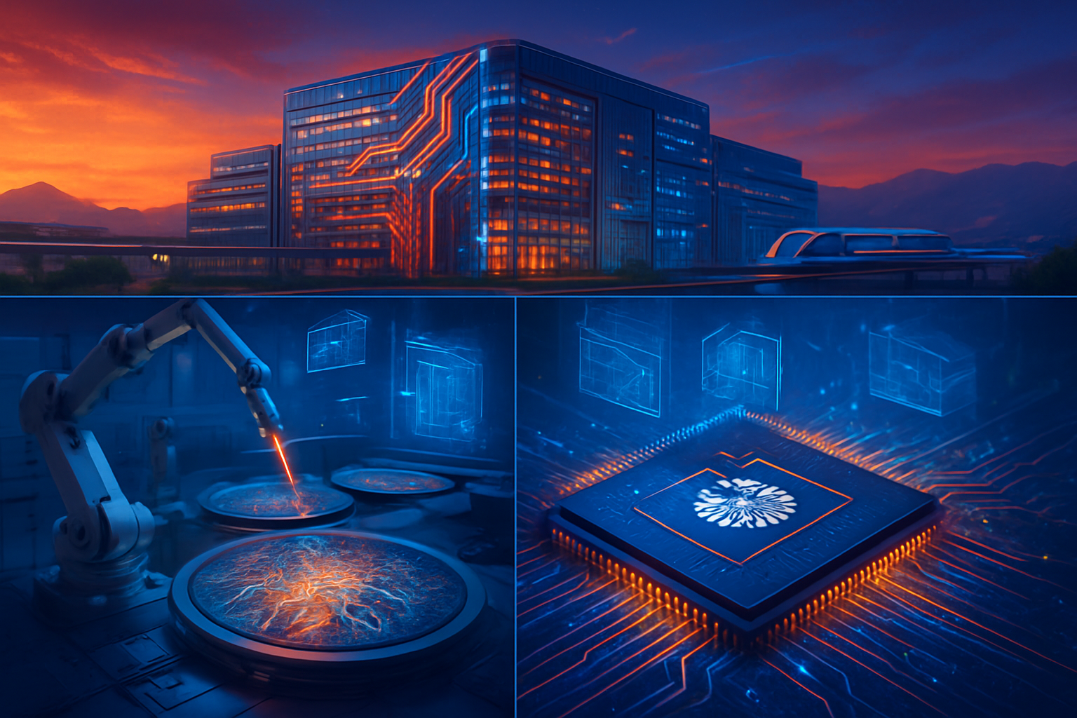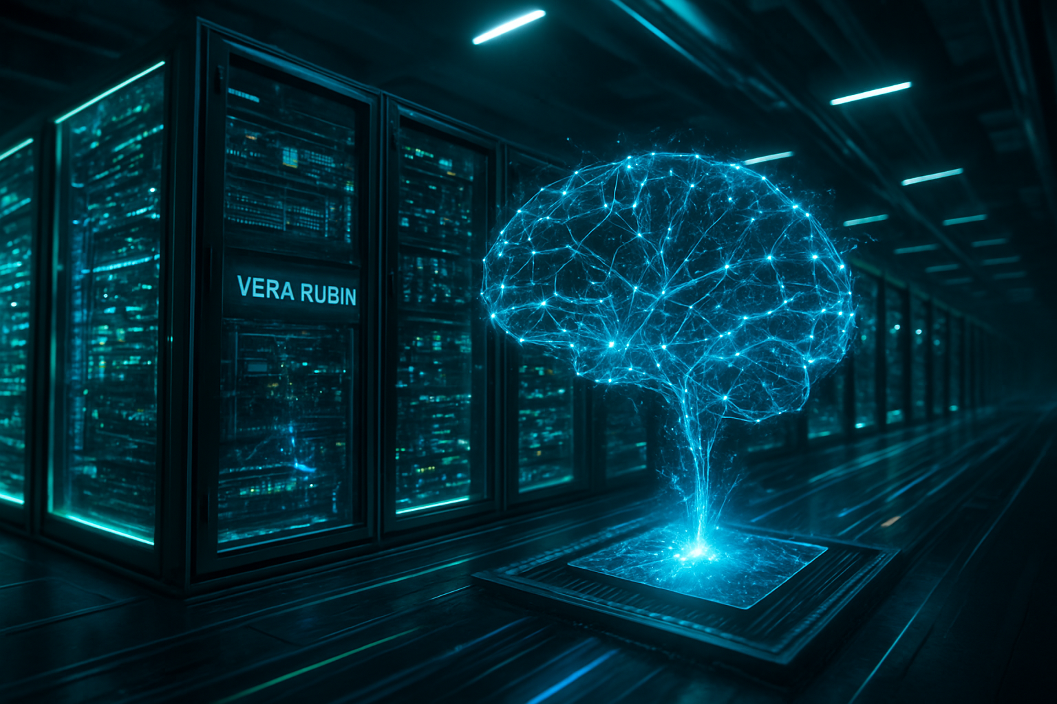
The landscape of artificial intelligence underwent a tectonic shift at CES 2026 as NVIDIA (NASDAQ: NVDA) officially took the wraps off its "Vera Rubin" architecture. Named after the legendary astronomer who provided the first evidence for dark matter, the Rubin platform is not merely an incremental update but a complete reimagining of the AI data center. With a transition to an annual release cadence, NVIDIA has signaled its intent to outpace the industry's exponential demand for compute, positioning Vera Rubin as the foundational infrastructure for the next generation of "agentic" AI—systems capable of complex reasoning and autonomous execution.
The announcement marks the arrival of what NVIDIA CEO Jensen Huang described as the "industrial phase of AI." By integrating cutting-edge 3nm manufacturing with the world’s first HBM4 memory implementation, the Vera Rubin platform aims to solve the twin challenges of the modern era: the massive computational requirements of trillion-parameter models and the economic necessity of real-time, low-latency inference. As the first systems prepare to ship later this year, the industry is already calling it the world's most powerful AI supercomputer platform, a claim backed by performance leaps that dwarf the previous Blackwell generation.
Technical Mastery: 3nm Silicon and the HBM4 Breakthrough
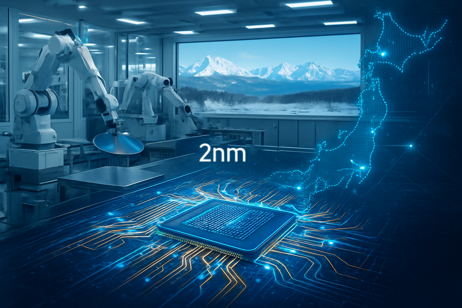
At the heart of the Vera Rubin architecture lies a feat of semiconductor engineering: a move to TSMC’s (NYSE: TSM) advanced 3nm process node. This transition has allowed NVIDIA to pack a staggering 336 billion transistors onto a single Rubin GPU, while the companion Vera CPU boasts 227 billion transistors of its own. This density isn't just for show; it translates into a 3.5x increase in training performance and a 5x boost in inference throughput compared to the Blackwell series. The flagship "Vera Rubin Superchip" combines one CPU and two GPUs on a single coherent package via the second-generation NVLink-C2C interconnect, offering a 1.8 TB/s memory space that allows the processors to work as a singular, massive brain.
The true "secret sauce" of the Rubin architecture, however, is its early adoption of HBM4 (High Bandwidth Memory 4). Each Rubin GPU supports up to 288GB of HBM4, delivering an aggregate bandwidth of 22 TB/s—nearly triple that of its predecessor. This massive memory pipe is essential for handling the "KV cache" requirements of long-context models, which have become the standard for enterprise AI. When coupled with the new NVLink 6 interconnect, which provides 3.6 TB/s of bi-directional bandwidth, entire racks of these chips function as a unified GPU. This hardware stack is specifically tuned for NVFP4 (NVIDIA Floating Point 4), a precision format that allows for high-accuracy reasoning at a fraction of the traditional power and memory cost.
Initial reactions from the research community have focused on NVIDIA’s shift from "chip-first" to "system-first" design. Industry analysts from Moor Insights & Strategy noted that by co-designing the ConnectX-9 SuperNIC and the Spectrum-6 Ethernet Switch alongside the Rubin silicon, NVIDIA has effectively eliminated the "data bottlenecks" that previously plagued large-scale clusters. Experts suggest that while competitors are still catching up to the Blackwell performance tiers, NVIDIA has effectively moved the goalposts into a realm where the network and memory architecture are just as critical as the FLOPS (floating-point operations per second) produced by the core.
The Market Shakeup: Hyperscalers and the "Superfactory" Race
The business implications of the Vera Rubin launch are already rippling through the Nasdaq. Microsoft (NASDAQ: MSFT) was the first to blink, announcing that its upcoming "Fairwater" AI superfactories—designed to host hundreds of thousands of GPUs—will be built exclusively around the Vera Rubin NVL72 platform. This rack-scale system integrates 72 Rubin GPUs and 36 Vera CPUs into a single liquid-cooled domain, delivering a jaw-core 3.6 exaflops of AI performance per rack. For cloud giants like Amazon (NASDAQ: AMZN) and Google (NASDAQ: GOOGL), the Vera Rubin architecture represents the only viable path to offering the "agentic reasoning" capabilities that their enterprise customers are now demanding.
Competitive pressure is mounting on Advanced Micro Devices (NASDAQ: AMD) and Intel (NASDAQ: INTC), both of whom had recently made strides in closing the gap with NVIDIA’s older H100 and H200 chips. By accelerating its roadmap to an annual cycle, NVIDIA is forcing competitors into a perpetual state of catch-up. Startups in the AI chip space are also feeling the heat; the Rubin architecture’s 10x reduction in inference token costs makes it difficult for boutique hardware manufacturers to compete on the economics of scale. If NVIDIA can deliver on its promise of making 100-trillion-parameter models economically viable, it will likely cement its 90%+ market share in the AI data center for the foreseeable future.
Furthermore, the Rubin launch has triggered a secondary gold rush in the data center infrastructure market. Because the Rubin NVL72 racks generate significantly more heat than previous generations, liquid cooling is no longer optional. This has led to a surge in demand for thermal management solutions from partners like Supermicro (NASDAQ: SMCI) and Dell Technologies (NYSE: DELL). Analysts expect that the capital expenditure (CapEx) for top-tier AI labs will continue to balloon as they race to replace Blackwell clusters with Rubin-based "SuperPODs" that can deliver 28.8 exaflops of compute in a single cluster.
Wider Significance: From Chatbots to Agentic Reasoners
Beyond the raw specs, the Vera Rubin architecture represents a fundamental shift in the AI landscape. We are moving past the era of "static chatbots" and into the era of "Agentic AI." These are models that don't just predict the next word but can plan, reason, and execute multi-step tasks over long periods. To do this, an AI needs massive "working memory" and the ability to process data in real-time. Rubin’s Inference Context Memory Storage Platform, powered by the BlueField-4 DPU, is specifically designed to manage the complex data states required for these autonomous agents to function without lagging or losing their "train of thought."
This development also addresses the growing concern over the "efficiency wall" in AI. While the raw power consumption of a Rubin rack is immense, its efficiency per token is revolutionary. By providing a 10x reduction in the cost of generating AI responses, NVIDIA is making it possible for AI to be integrated into every aspect of software—from real-time coding assistants that understand entire million-line codebases to scientific models that can simulate molecular biology in real-time. This mirrors the transition from mainframe computers to the internet era; the "supercomputer" is no longer a distant resource but the engine behind every click and query.
However, the sheer scale of the Vera Rubin platform has also reignited debates about the "AI Divide." Only the wealthiest nations and corporations can afford to deploy Rubin SuperPODs at scale, potentially centralizing the most advanced "reasoning" capabilities in the hands of a few. Comparisons are being drawn to the Apollo program or the Manhattan Project; the Vera Rubin architecture is essentially a piece of "Big Science" infrastructure that happens to be owned by a private corporation. As we look at the progress from the first GPT models to the trillion-parameter behemoths Rubin will support, the milestone is clear: we have reached the point where hardware is no longer the bottleneck for artificial general intelligence (AGI).
The Road Ahead: What Follows Rubin?
The horizon for NVIDIA does not end with the standard Rubin chip. Looking toward 2027, the company has already teased a "Rubin Ultra" variant, which is expected to push HBM4 capacities even further and introduce more specialized "AI Foundry" features. The move to an annual cadence means that by the time many companies have fully deployed their Rubin racks, the successor architecture—rumored to be focused on "Physical AI" and robotics—will already be in the sampling phase. This relentless pace is designed to keep NVIDIA at the center of the "sovereign AI" movement, where nations build their own domestic compute capacity.
In the near term, the focus will shift to software orchestration. While the Rubin hardware is a marvel, the challenge now lies in the "NVIDIA NIM" (NVIDIA Inference Microservices) and the CUDA-X libraries that must manage the complexity of agentic workflows. Experts predict that the next major breakthrough will not be a larger model, but a "system of models" running concurrently on a Rubin Superchip, where one model plans, another executes, and a third audits the results—all in real-time. The challenge for developers in 2026 will be learning how to harness this much power without drowning in the complexity of the data it generates.
A New Benchmark for AI History
The unveiling of the Vera Rubin architecture at CES 2026 will likely be remembered as the moment the "AI Summer" turned into a permanent climate shift. By delivering a platform that is 5x faster for inference and capable of supporting 10-trillion-parameter models with ease, NVIDIA has removed the final hardware barriers to truly autonomous AI. The combination of 3nm precision and HBM4 bandwidth sets a new gold standard that will define data center construction for the next several years.
As we move through February 2026, all eyes will be on the first production shipments. The significance of this development cannot be overstated: it is the "engine" for the next industrial revolution. For the tech industry, the message is clear: the race for AI supremacy has shifted from who has the best algorithm to who has the most "Rubins" in their rack. What to watch for in the coming months is the "Rubin Effect" on global productivity—as these systems go online, the speed of AI-driven discovery in medicine, materials science, and software is expected to accelerate at a rate never before seen in human history.
This content is intended for informational purposes only and represents analysis of current AI developments.
TokenRing AI delivers enterprise-grade solutions for multi-agent AI workflow orchestration, AI-powered development tools, and seamless remote collaboration platforms.
For more information, visit https://www.tokenring.ai/.