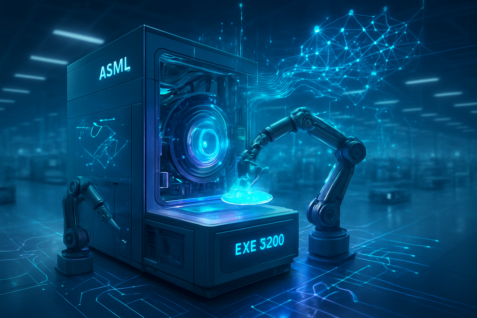
In a decisive move that reshapes the competitive landscape of artificial intelligence infrastructure, Samsung Electronics (KRX: 005930) has officially cleared the final quality and reliability tests for its 6th-generation High Bandwidth Memory (HBM4) from both NVIDIA (NASDAQ: NVDA) and AMD (NASDAQ: AMD). As of late January 2026, this breakthrough signals a major reversal of fortune for the South Korean tech giant, which had spent much of the previous two years trailing behind its chief rival, SK Hynix (KRX: 000660), in the race to supply the memory chips essential for generative AI.
The validation of Samsung’s HBM4 is not merely a logistical milestone; it is a technological leap that promises to unlock the next tier of AI performance. By securing approval for NVIDIA’s upcoming "Vera Rubin" platform and AMD’s MI450 accelerators, Samsung has positioned itself as a critical pillar for the 2026 AI hardware cycle. Industry insiders suggest that the successful qualification has already led to the conversion of multiple production lines at Samsung’s P4 and P5 facilities in Pyeongtaek to meet the explosive demand from hyperscalers like Google and Microsoft.
Technical Specifications: The 11Gbps Frontier
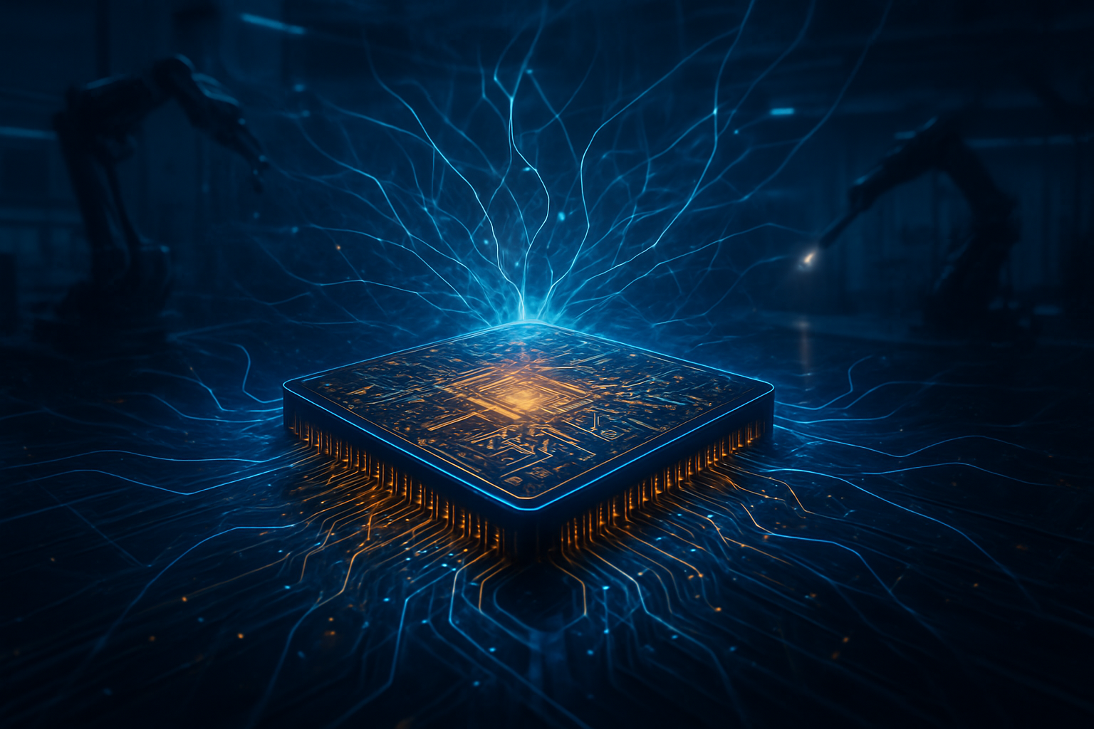
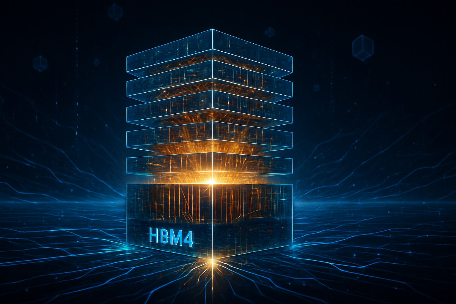
The defining characteristic of Samsung’s HBM4 is its unprecedented data transfer rate. While the industry standard for HBM3E hovered around 9.2 to 10 Gbps, Samsung’s latest modules have achieved stable speeds of 11.7 Gbps per pin. This 11Gbps+ threshold is achieved through the implementation of Samsung’s 6th-generation 10nm-class (1c) DRAM process. This marks the first time a memory manufacturer has successfully integrated 1c DRAM into an HBM stack, providing a 20% improvement in power efficiency and significantly higher bit density than the 1b DRAM currently utilized by competitors.
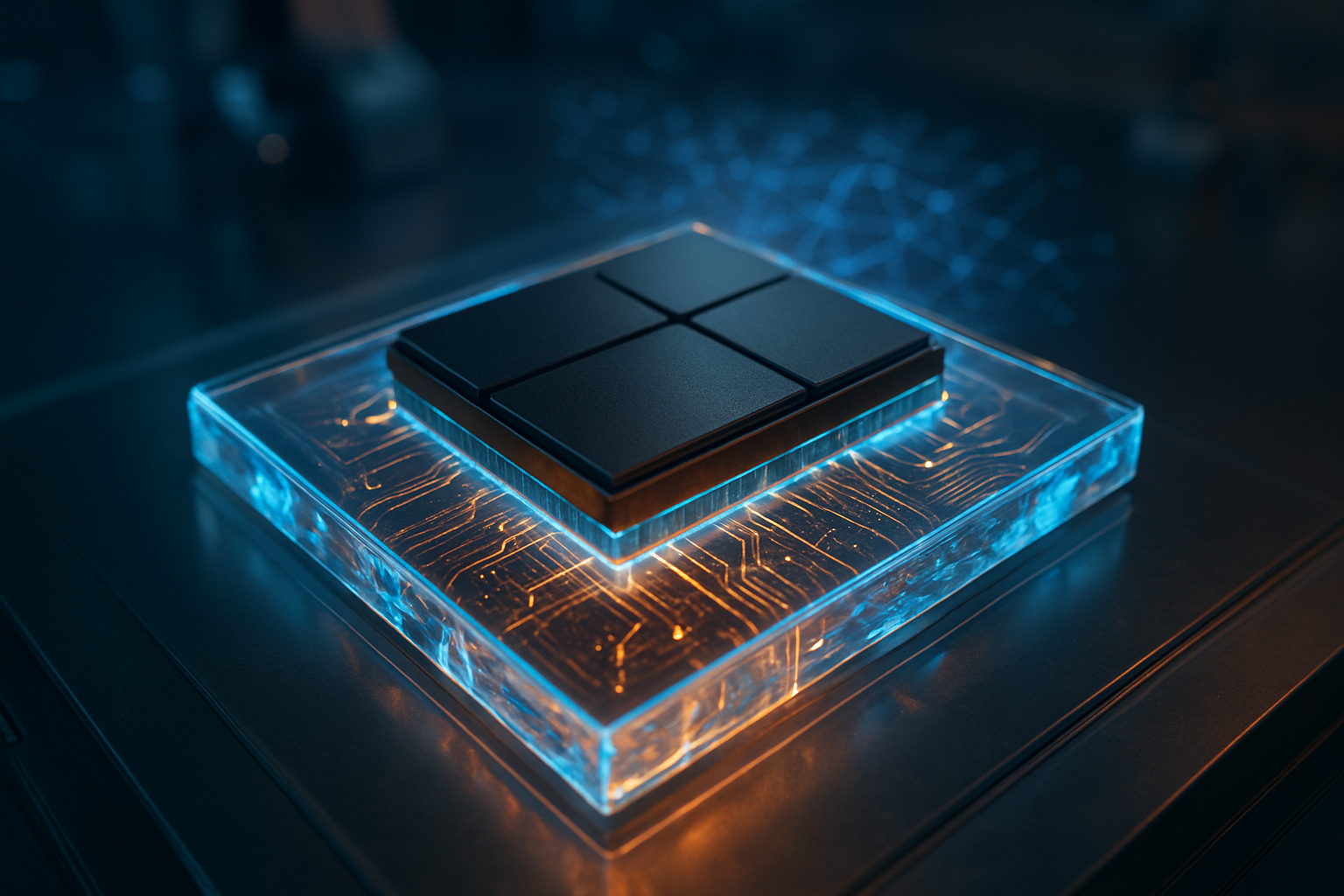
Unlike previous generations, HBM4 features a fundamental architectural shift: the integration of a logic base die. Samsung has leveraged its unique position as the world’s only company with both leading-edge memory and foundry capabilities to produce a "turnkey" solution. Utilizing its own 4nm foundry process for the logic die, Samsung has eliminated the need to outsource to third-party foundries like TSMC. This vertical integration allows for tighter architectural optimization, superior thermal management, and a more streamlined supply chain, addressing the heat dissipation issues that have plagued high-density AI memory stacks in the past.
Initial reactions from the AI research community and semiconductor analysts have been overwhelmingly positive. "Samsung’s move to a 4nm logic die in-house is a game-changer," noted one senior analyst at the Silicon Valley Semiconductor Institute. "By controlling the entire stack from the DRAM cells to the logic interface, they have managed to reduce latency and power draw at a level that was previously thought impossible for 12-layer and 16-layer stacks."
Market Displacement: Closing the Gap with SK Hynix
For the past three years, SK Hynix has enjoyed a near-monopoly on the high-end HBM market, particularly through its exclusive "One-Team" alliance with NVIDIA. However, Samsung’s late-January breakthrough has effectively ended this era of undisputed dominance. While SK Hynix still holds a projected 54% market share for 2026 due to earlier contract wins, Samsung is aggressively clawing back territory, targeting a 30% or higher share by the end of the fiscal year.
The competitive implications for the "Big Three"—Samsung, SK Hynix, and Micron (NASDAQ: MU)—are profound. Samsung’s ability to clear tests for both NVIDIA and AMD simultaneously creates a supply cushion for AI chipmakers who have been desperate to diversify their sources. For AMD, Samsung’s HBM4 is the "secret sauce" for the MI450, allowing them to offer a competitive alternative to NVIDIA’s Vera Rubin platform in terms of raw memory bandwidth. This shift prevents a single-supplier bottleneck, which has historically inflated prices for data center operators.
Strategic advantages are also shifting toward a multi-vendor model. Tech giants like Meta and Amazon are reportedly pivoting their procurement strategies to favor Samsung’s turnkey solution, which offers a faster time-to-market compared to the collaborative Hynix-TSMC model. This diversification is seen as a vital step in stabilizing the global AI supply chain, which remains under immense pressure as LLM (Large Language Model) training requirements continue to scale exponentially.
Broader Significance: The Vera Rubin Era and Global Supply
The timing of Samsung’s breakthrough is meticulously aligned with the broader AI landscape's transition to "Hyper-Scale" inference. As the industry moves toward NVIDIA’s Vera Rubin architecture, the demand for memory bandwidth has nearly doubled. A Rubin-based system equipped with eight stacks of Samsung’s HBM4 can reach an aggregate bandwidth of 22 TB/s. This allows for the real-time processing of models with tens of trillions of parameters, effectively moving the needle from "generative chat" to "autonomous reasoning agents."
However, this milestone also brings potential concerns to the forefront. The sheer volume of capacity required for HBM4 production has led to a "cannibalization" of standard DRAM production lines. As Samsung and SK Hynix shift their focus to AI memory, prices for consumer-grade DDR5 and mobile LPDDR6 are expected to rise sharply in late 2026. This highlights a growing divide between the AI-industrial complex and the consumer electronics market, where AI-specific hardware is increasingly prioritized over general-purpose computing.
Comparatively, this milestone is being likened to the transition from 2D to 3D NAND flash a decade ago. It represents a "point of no return" where memory is no longer a passive storage component but an active participant in the compute cycle. The integration of logic directly into the memory stack signifies the first major step toward "Processing-in-Memory" (PIM), a long-held dream of computer scientists that is finally becoming a commercial reality.
Future Outlook: Mass Production and GTC 2026
The immediate next step for Samsung is the official public debut of the HBM4 modules at NVIDIA GTC 2026, scheduled for March 16–19. This event is expected to feature live demonstrations of the Vera Rubin platform, with Samsung’s memory powering the world’s most advanced AI training clusters. Following the debut, full-scale mass production is slated to ramp up in the second quarter of 2026, with the first server systems reaching hyperscale customers by August.
Looking further ahead, experts predict that Samsung will use its current momentum to fast-track the development of HBM4E (Enhanced). While HBM4 is just entering the market, the roadmap for 2027 already includes 20-layer stacks and even higher clock speeds. The challenge remains in maintaining yields; at 11.7 Gbps, the margin for error in the Through-Silicon Via (TSV) manufacturing process is razor-thin. If Samsung can maintain its current yield rates as it scales, it could potentially reclaim the title of the world’s leading HBM supplier by 2027.
A New Chapter in the AI Memory War
In summary, Samsung’s successful navigation of the NVIDIA and AMD qualification process marks a historic comeback. By delivering 11Gbps speeds and a vertically integrated 4nm logic die, Samsung has proved that its "all-under-one-roof" strategy is a viable—and perhaps superior—alternative to the collaborative models of its rivals. This development ensures that the AI industry has the memory bandwidth necessary to power the next generation of reasoning-capable artificial intelligence.
In the coming weeks, the industry will be watching for the official pricing structures and the first performance benchmarks of the Vera Rubin platform at GTC 2026. While SK Hynix remains a formidable opponent with deep ties to the AI ecosystem, Samsung has officially closed the gap, turning a one-horse race into a high-speed pursuit that will define the future of computing for years to come.
This content is intended for informational purposes only and represents analysis of current AI developments.
TokenRing AI delivers enterprise-grade solutions for multi-agent AI workflow orchestration, AI-powered development tools, and seamless remote collaboration platforms.
For more information, visit https://www.tokenring.ai/.