San Francisco, CA – November 5, 2025 – The artificial intelligence landscape is undergoing a profound transformation, with the AI on Edge Semiconductor Market emerging as a pivotal force driving this evolution. This specialized segment, focused on bringing AI processing capabilities directly to devices and local networks, is experiencing an unprecedented surge, poised to redefine how intelligent systems operate across every industry. With projections indicating a monumental leap to USD 9.3 Billion by 2031, the market's rapid expansion underscores a fundamental shift in AI deployment strategies, prioritizing real-time responsiveness, enhanced data privacy, and operational autonomy.
This explosive growth is not merely a statistical anomaly but a reflection of critical demands unmet by traditional cloud-centric AI models. As the world becomes increasingly saturated with IoT devices, from smart home appliances to industrial sensors and autonomous vehicles, the need for instantaneous data analysis and decision-making at the source has never been more pressing. AI on Edge semiconductors are the silicon backbone enabling this new era, allowing devices to act intelligently and independently, even in environments with limited or intermittent connectivity. This decentralization of AI processing promises to unlock new levels of efficiency, security, and innovation, making AI truly ubiquitous and fundamentally reshaping the broader technological ecosystem.
The Silicon Brains at the Edge: Technical Underpinnings of a Revolution
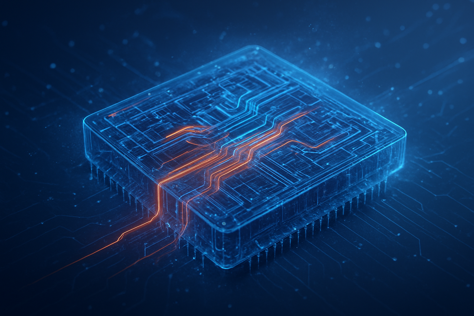
The technical advancements propelling the AI on Edge Semiconductor Market represent a significant departure from previous AI processing paradigms. Historically, complex AI tasks, particularly the training of large models, have been confined to powerful, centralized cloud data centers. Edge AI, however, focuses on efficient inference—the application of trained AI models to new data—directly on the device. This is achieved through highly specialized hardware designed for low power consumption, compact form factors, and optimized performance for specific AI workloads.
At the heart of this innovation are Neural Processing Units (NPUs), AI Accelerators, and specialized System-on-Chip (SoC) architectures. Unlike general-purpose CPUs or even GPUs (which are excellent for parallel processing but can be power-hungry), NPUs are custom-built to accelerate neural network operations like matrix multiplications and convolutions, the fundamental building blocks of deep learning. These chips often incorporate dedicated memory, efficient data pathways, and innovative computational structures that allow them to execute AI models with significantly less power and lower latency than their cloud-based counterparts. For instance, many edge AI chips can perform hundreds of trillions of operations per second (TOPS) within a power envelope of just a few watts, a feat previously unimaginable for on-device AI. This contrasts sharply with cloud AI, which relies on high-power server-grade GPUs or custom ASICs in massive data centers, incurring significant energy and cooling costs. The initial reactions from the AI research community and industry experts highlight the critical role these advancements play in democratizing AI, making sophisticated intelligence accessible to a wider range of applications and environments where cloud connectivity is impractical or undesirable.
Reshaping the Corporate Landscape: Beneficiaries and Battlefield
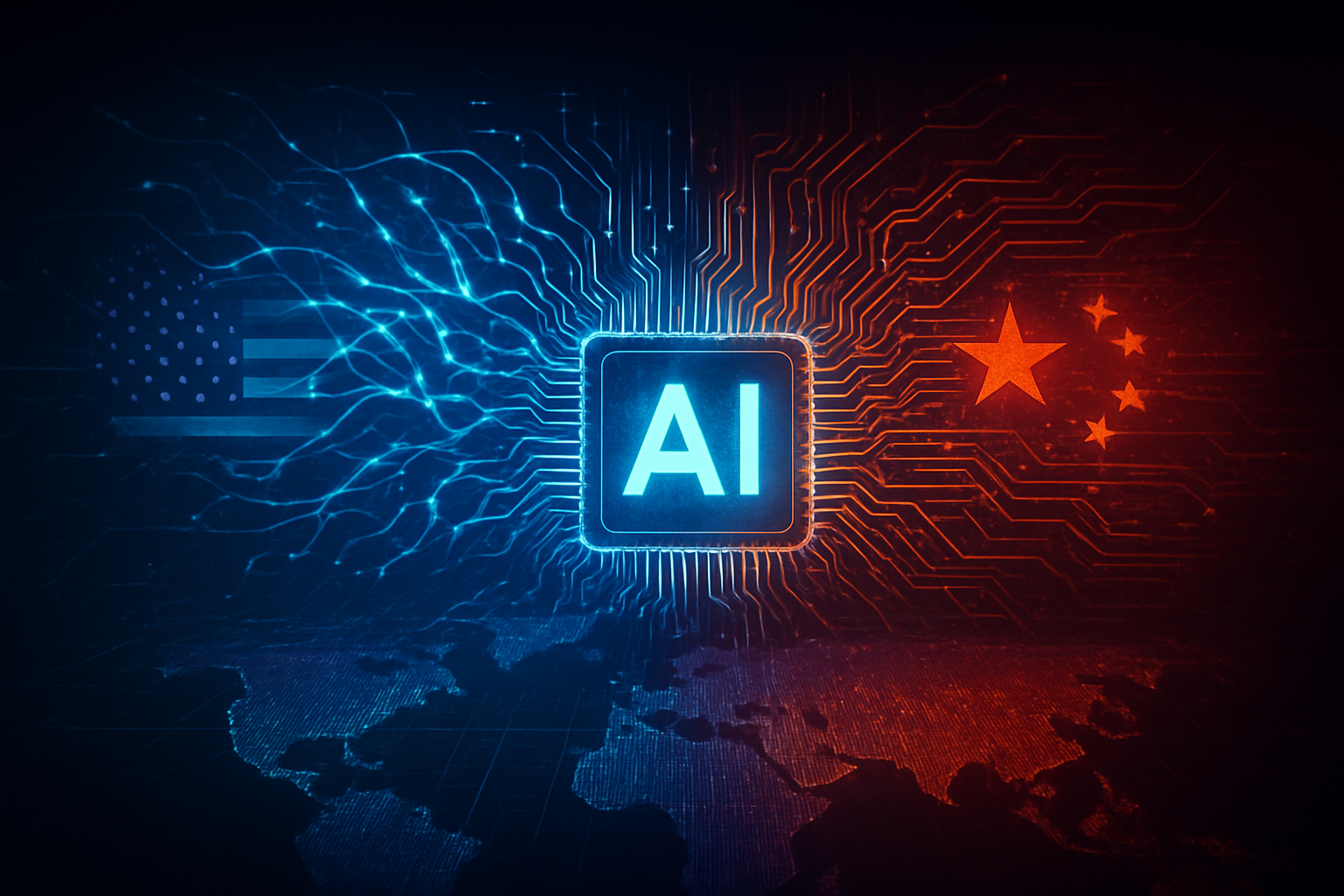
The surging growth of the AI on Edge Semiconductor Market is creating a new competitive battleground, with significant implications for established tech giants, semiconductor manufacturers, and a burgeoning ecosystem of startups. Companies poised to benefit most are those with strong intellectual property in chip design, advanced manufacturing capabilities, and strategic partnerships across the AI value chain.
Traditional semiconductor powerhouses like NVIDIA (NASDAQ: NVDA), while dominant in cloud AI with its GPUs, are actively expanding their edge offerings, developing platforms like Jetson for robotics and embedded AI. Intel (NASDAQ: INTC) is also a key player, leveraging its Movidius vision processing units and OpenVINO toolkit to enable edge AI solutions across various industries. Qualcomm (NASDAQ: QCOM), a leader in mobile processors, is extending its Snapdragon platforms with dedicated AI Engines for on-device AI in smartphones, automotive, and IoT. Beyond these giants, companies like Arm Holdings (NASDAQ: ARM), whose architecture underpins many edge devices, are crucial, licensing their low-power CPU and NPU designs to a vast array of chipmakers. Startups specializing in ultra-efficient AI silicon, such as Hailo and Mythic, are also gaining traction, offering innovative architectures that push the boundaries of performance-per-watt for edge inference. This competitive landscape is driving rapid innovation, as companies vie for market share in a sector critical to the future of ubiquitous AI. The potential disruption to existing cloud-centric business models is substantial, as more processing shifts to the edge, potentially reducing reliance on costly cloud infrastructure for certain AI workloads. This strategic advantage lies in enabling new product categories and services that demand real-time, secure, and autonomous AI capabilities.
The Broader Canvas: AI on Edge in the Grand Scheme of Intelligence
The rise of the AI on Edge Semiconductor Market is more than just a technological advancement; it represents a fundamental shift in the broader AI landscape, addressing critical limitations and opening new frontiers. This development fits squarely into the trend of distributed intelligence, where AI capabilities are spread across networks rather than concentrated in singular hubs. It's a natural evolution from the initial focus on large-scale cloud AI training, complementing it by enabling efficient, real-world application of those trained models.
The impacts are far-reaching. In industries like autonomous driving, edge AI is non-negotiable for instantaneous decision-making, ensuring safety and reliability. In healthcare, it enables real-time patient monitoring and diagnostics on wearable devices, protecting sensitive data. Manufacturing benefits from predictive maintenance and quality control at the factory floor, improving efficiency and reducing downtime. Potential concerns, however, include the complexity of managing and updating AI models across a vast number of edge devices, ensuring robust security against tampering, and the ethical implications of autonomous decision-making in critical applications. Compared to previous AI milestones, such as the breakthroughs in deep learning for image recognition or natural language processing, the AI on Edge movement marks a pivotal transition from theoretical capability to practical, pervasive deployment. It’s about making AI not just intelligent, but also agile, resilient, and deeply integrated into the fabric of our physical world, bringing the intelligence closer to the point of action.
Horizon Scanning: The Future of Edge AI and Beyond
Looking ahead, the trajectory of the AI on Edge Semiconductor Market points towards an era of increasingly sophisticated and pervasive intelligent systems. Near-term developments are expected to focus on further enhancing the energy efficiency and computational power of edge AI chips, enabling more complex neural networks to run locally. We will likely see a proliferation of specialized architectures tailored for specific domains, such as vision processing for smart cameras, natural language processing for voice assistants, and sensor fusion for robotics.
Long-term, the vision includes truly autonomous edge devices capable of continuous learning and adaptation without constant cloud connectivity, moving beyond mere inference to on-device training or federated learning approaches. Potential applications are vast and transformative: fully autonomous delivery robots navigating complex urban environments, personalized healthcare devices providing real-time medical insights, smart cities with self-optimizing infrastructure, and highly efficient industrial automation systems. Challenges that need to be addressed include the standardization of edge AI software stacks, robust security protocols for distributed AI, and the development of tools for efficient model deployment and lifecycle management across diverse hardware. Experts predict a future where hybrid AI architectures, seamlessly integrating cloud training with edge inference, will become the norm, creating a resilient and highly scalable intelligent ecosystem. The continuous miniaturization and power reduction of AI capabilities will unlock unforeseen use cases, pushing the boundaries of what connected, intelligent devices can achieve.
The Intelligent Edge: A New Chapter in AI History
The surging growth of the AI on Edge Semiconductor Market represents a critical inflection point in the history of artificial intelligence. It signifies a maturation of AI from a cloud-bound technology to a pervasive, on-device intelligence that is transforming industries and daily life. The market's projected growth to USD 9.3 Billion by 2031 underscores its pivotal role in enabling real-time decision-making, bolstering data privacy, and optimizing resource utilization across an ever-expanding array of connected devices.
The key takeaways are clear: Edge AI is indispensable for the proliferation of IoT, the demand for instantaneous responses, and the drive towards more secure and sustainable AI deployments. This development is not just enhancing existing technologies but is actively catalyzing the creation of entirely new products and services, fostering an "AI Supercycle" that will continue to drive innovation in both hardware and software. Its significance in AI history lies in democratizing intelligence, making it more accessible, reliable, and deeply integrated into the physical world. As we move forward, the focus will be on overcoming challenges related to standardization, security, and lifecycle management of edge AI models. What to watch for in the coming weeks and months are continued breakthroughs in chip design, the emergence of new industry partnerships, and the deployment of groundbreaking edge AI applications across sectors ranging from automotive to healthcare. The intelligent edge is not just a trend; it is the foundation of the next generation of AI-powered innovation.
This content is intended for informational purposes only and represents analysis of current AI developments.
TokenRing AI delivers enterprise-grade solutions for multi-agent AI workflow orchestration, AI-powered development tools, and seamless remote collaboration platforms.
For more information, visit https://www.tokenring.ai/.