The global race for artificial intelligence (AI) dominance is heating up, and at its very core lies the unassuming yet utterly critical semiconductor chip. These tiny powerhouses are not merely components; they are the foundational bedrock upon which national security, economic competitiveness, and corporate leadership in the rapidly evolving AI landscape are being built. As of November 3, 2025, advancements in chip technology are not just facilitating AI progress; they are dictating its pace, scale, and very capabilities, making the control and innovation in semiconductor design and manufacturing synonymous with leadership in artificial intelligence itself.
The immediate significance of these advancements is profound. Specialized AI accelerators are enabling faster training and deployment of increasingly complex AI models, including the sophisticated Large Language Models (LLMs) and generative AI that are transforming industries worldwide. This continuous push for more powerful, efficient, and specialized silicon is broadening AI's applications into numerous sectors, from autonomous vehicles to healthcare diagnostics, while simultaneously driving down the cost of implementing AI at scale.
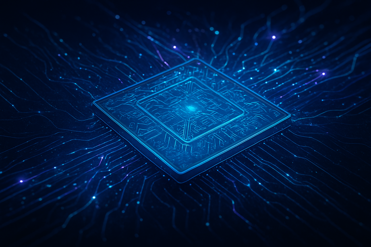
Engineering the Future: Technical Marvels in AI Silicon
The escalating computational demands of modern AI, particularly deep learning and generative AI, have spurred an unprecedented era of innovation in AI chip technology. This evolution moves significantly beyond previous approaches that relied heavily on traditional Central Processing Units (CPUs), which are less efficient for the massive parallel computational tasks inherent in AI.
Today's AI chips boast impressive technical specifications. Manufacturers are pushing the boundaries of transistor size, with chips commonly built on 7nm, 5nm, 4nm, and even 3nm process nodes, enabling higher density, improved power efficiency, and faster processing speeds. Performance is measured in TFLOPS (teraFLOPS) for high-precision training and TOPS (Trillions of Operations Per Second) for lower-precision inference. For instance, NVIDIA Corporation (NASDAQ: NVDA) H100 GPU offers up to 9 times the performance of its A100 predecessor, while Qualcomm Technologies, Inc. (NASDAQ: QCOM) Cloud AI 100 achieves up to 400 TOPS of INT8 inference throughput. High-Bandwidth Memory (HBM) is also critical, with NVIDIA's A100 GPUs featuring 80GB of HBM2e memory and bandwidths exceeding 2,000 GB/s, and Apple Inc. (NASDAQ: AAPL) M5 chip offering a unified memory bandwidth of 153GB/s.
Architecturally, the industry is seeing a shift towards highly specialized designs. Graphics Processing Units (GPUs), spearheaded by NVIDIA, continue to innovate with architectures like Hopper, which includes specialized Tensor Cores and Transformer Engines. Application-Specific Integrated Circuits (ASICs), exemplified by Alphabet Inc. (NASDAQ: GOOGL) (NASDAQ: GOOG) Tensor Processing Units (TPUs), offer the highest efficiency for specific AI tasks. Neural Processing Units (NPUs) are increasingly integrated into edge devices for low-latency, energy-efficient on-device AI. A more radical departure is neuromorphic computing, which aims to mimic the human brain's structure, integrating computation and memory to overcome the "memory wall" bottleneck of traditional Von Neumann architectures.
Furthermore, heterogeneous integration and chiplet technology are addressing the physical limits of traditional semiconductor scaling. Heterogeneous integration involves assembling multiple dissimilar semiconductor components (logic, memory, I/O) into a single package, allowing for optimal performance and cost. Chiplet technology breaks down large processors into smaller, specialized components (chiplets) interconnected within a single package, offering scalability, flexibility, improved yield rates, and faster time-to-market. Companies like Advanced Micro Devices, Inc. (NASDAQ: AMD) and Intel Corporation (NASDAQ: INTC) are heavy investors in chiplet technology for their AI and HPC accelerators. Initial reactions from the AI research community are overwhelmingly positive, viewing these advancements as a "transformative phase" and the dawn of an "AI Supercycle," though challenges like data requirements, energy consumption, and talent shortages remain.
Corporate Chessboard: Shifting Power Dynamics in the AI Chip Arena
The advancements in AI chip technology are driving a significant reordering of the competitive landscape for AI companies, tech giants, and startups alike. This "AI Supercycle" is characterized by an insatiable demand for computational power, leading to unprecedented investment and strategic maneuvering.
NVIDIA Corporation (NASDAQ: NVDA) remains a dominant force, with its GPUs and CUDA software platform being the de facto standard for AI training and generative AI. The company's "AI factories" strategy has solidified its market leadership, pushing its valuation to an astounding $5 trillion in 2025. However, this dominance is increasingly challenged by Advanced Micro Devices, Inc. (NASDAQ: AMD), which is developing new AI chips like the Instinct MI350 series and building its ROCm software ecosystem as an alternative to CUDA. Intel Corporation (NASDAQ: INTC) is also aggressively pushing its foundry services and AI chip portfolio, including Gaudi accelerators.
Perhaps the most significant competitive implication is the trend of major tech giants—hyperscalers like Alphabet Inc. (NASDAQ: GOOGL) (NASDAQ: GOOG), Amazon.com, Inc. (NASDAQ: AMZN), Microsoft Corporation (NASDAQ: MSFT), Meta Platforms, Inc. (NASDAQ: META), and Apple Inc. (NASDAQ: AAPL)—developing their own custom AI silicon. Google's TPUs, Amazon's Trainium/Inferentia, Microsoft's Azure Maia 100, Apple's Neural Engine Unit, and Meta's in-house AI training chips are all strategic moves to reduce dependency on external suppliers, optimize performance for their specific cloud services, diversify supply chains, and increase profit margins. This shift towards vertical integration gives these companies greater control and a strategic advantage in the highly competitive cloud AI market.
This rapid innovation also disrupts existing products and services. Companies unable to adapt to the latest hardware capabilities face quicker obsolescence, necessitating continuous investment in new hardware. Conversely, specialized AI chips unlock new classes of applications across various sectors, from advanced driver-assistance systems in automotive to improved medical imaging. While venture capital pours into silicon startups, the immense costs and resources needed for advanced chip development could lead to a concentration of power among a few dominant players, raising concerns about competition and accessibility for smaller entities. Companies are now prioritizing supply chain resilience, strategic partnerships, and continuous R&D to maintain or gain market positioning.
A New Era: Broader Implications and Geopolitical Fault Lines
The advancements in AI chip technology are not merely technical feats; they represent a foundational shift with profound implications for the broader AI landscape, global economies, societal structures, and international relations. This "AI Supercycle" is creating a virtuous cycle where hardware development and AI progress are deeply symbiotic.
These specialized processors are enabling the shift to complex AI models, particularly Large Language Models (LLMs) and generative AI, which require unprecedented computational power. They are also crucial for expanding AI to the "edge," allowing real-time, low-power processing directly on devices like IoT sensors and autonomous vehicles. In a fascinating self-referential loop, AI itself has become an indispensable tool in designing and manufacturing advanced chips, optimizing layouts and accelerating design cycles. This marks a fundamental shift where AI is a co-creator of its own hardware destiny.
Economically, the global AI chip market is experiencing exponential growth, projected to soar past $150 billion in 2025 and potentially reach $400 billion by 2027. This has fueled an investment frenzy, concentrating wealth in companies like NVIDIA Corporation (NASDAQ: NVDA), which has become a dominant force. AI is viewed as an emergent general-purpose technology, capable of boosting productivity across the economy and creating new industries, similar to past innovations like the internet. Societally, AI chip advancements are enabling transformative applications in healthcare, smart cities, climate modeling, and robotics, while also democratizing AI access through devices like the Raspberry Pi 500+.
However, this rapid progress comes with significant concerns. The energy consumption of modern AI systems is immense; data centers supporting AI operations are projected to consume 1,580 terawatt-hours per year by 2034, comparable to India's entire electricity consumption. This raises environmental concerns and puts strain on power grids. Geopolitically, the competition for technological supremacy in AI and semiconductor manufacturing has intensified, notably between the United States and China. Stringent export controls, like those implemented by the U.S., aim to impede China's AI advancement, highlighting critical chokepoints in the global supply chain. Taiwan Semiconductor Manufacturing Company (NYSE: TSM), producing over 90% of the world's most sophisticated chips, remains a pivotal yet vulnerable player. The high costs of designing and manufacturing advanced semiconductors also create barriers to entry, concentrating power among a few dominant players and exacerbating a growing talent gap.
Compared to previous AI milestones, this era is unique. While Moore's Law historically drove general-purpose computing, its slowdown has pushed the industry towards specialized architectures for AI, offering efficiency gains equivalent to decades of Moore's Law improvements for CPUs when applied to AI algorithms. The sheer growth rate of computational power required for AI training, doubling approximately every four months, far outpaces previous computational advancements, solidifying the notion that specialized hardware is now the primary engine of AI progress.
The Horizon: Anticipating AI Chip's Next Frontiers
The future of AI chip technology promises a relentless pursuit of efficiency, specialization, and integration, alongside the emergence of truly transformative computing paradigms. Both near-term refinements and long-term, radical shifts are on the horizon.
In the near term (1-3 years), we can expect continued advancements in hybrid chips, combining various processing units for optimized workloads, and a significant expansion of advanced packaging techniques like High Bandwidth Memory (HBM) customization and modular manufacturing using chiplets. The Universal Chiplet Interconnect Express (UCIe) standard will see broader adoption, offering flexibility and cost-effectiveness. Edge AI and on-device compute will become even more prevalent, with Neural Processing Units (NPUs) growing in importance for real-time applications in smartphones, IoT devices, and autonomous systems. Major tech companies like Meta Platforms, Inc. (NASDAQ: META) will continue to develop their own custom AI training chips, such as the Meta Training and Inference Accelerator (MTIA), while NVIDIA Corporation (NASDAQ: NVDA) is rapidly advancing its GPU technology with the anticipated "Vera Rubin" GPUs. Crucially, AI itself will be increasingly leveraged in chip design, with AI-powered Electronic Design Automation (EDA) tools automating tasks and optimizing power, performance, and area.
Longer term, truly revolutionary technologies are on the horizon. Neuromorphic computing, aiming to mimic the human brain's neural structure, promises significant efficiency gains and faster computing speeds. Optical computing, which uses light particles instead of electricity for data transfer, could multiply processing power while drastically cutting energy demand. Quantum computing, though still largely in the research phase, holds immense potential for AI, capable of performing calculations at lightning speed and reducing AI model training times from years to minutes. Companies like Cerebras Systems are also pushing the boundaries with wafer-scale engines (WSEs), massive chips with an incredible number of cores designed for extreme parallelism.
These advancements will enable a broad spectrum of new applications. Generative AI and Large Language Models (LLMs) will become even more sophisticated and pervasive, accelerating parallel processing for neural networks. Autonomous systems will benefit immensely from chips capable of capturing and processing vast amounts of data in near real-time. Edge AI will proliferate across consumer electronics, industrial applications, and the automotive sector, enhancing everything from object detection to natural language processing. AI will also continue to improve chip manufacturing itself through predictive maintenance and real-time process optimization.
However, significant challenges persist. The immense energy consumption of high-performance AI workloads remains a critical concern, pushing for a renewed focus on energy-efficient hardware and sustainable AI strategies. The enormous costs of designing and manufacturing advanced chips create high barriers to entry, exacerbating supply chain vulnerabilities due to heavy dependence on a few key manufacturers and geopolitical tensions. Experts predict that the next decade will be dominated by AI, with hardware at the epicenter of the next global investment cycle. They foresee continued architectural evolution to overcome current limitations, leading to new trillion-dollar opportunities, and an intensified focus on sustainability and national "chip sovereignty" as governments increasingly regulate chip exports and domestic manufacturing.
The AI Supercycle: A Transformative Era Unfolding
The symbiotic relationship between semiconductors and Artificial Intelligence has ushered in a transformative era, often dubbed the "AI Supercycle." Semiconductors are no longer just components; they are the fundamental infrastructure enabling AI's remarkable progress and dictating the pace of innovation across industries.
The key takeaway is clear: specialized AI accelerators—GPUs, ASICs, NPUs—are essential for handling the immense computational demands of modern AI, particularly the training and inference of complex deep neural networks and generative AI. Furthermore, AI itself has evolved beyond being merely a software application consuming hardware; it is now actively shaping the very infrastructure that powers its evolution, integrated across the entire semiconductor value chain from design to manufacturing. This foundational shift has elevated specialized hardware to a central strategic asset, reaffirming its competitive importance in an AI-driven world.
The long-term impact of this synergy will be pervasive AI, deeply integrated into nearly every facet of technology and daily life. We can anticipate autonomous chip design, where AI explores and optimizes architectures beyond human capabilities, and a renewed focus on energy efficiency to address the escalating power consumption of AI. This continuous feedback loop will also accelerate the development of revolutionary computing paradigms like neuromorphic and quantum computing, opening doors to solving currently intractable problems. The global AI chip market is projected for explosive growth, with some estimates reaching $460.9 billion by 2034, underscoring its pivotal role in the global economy and geopolitical landscape.
In the coming weeks and months, watch for an intensified push towards even more specialized AI chips and custom silicon from major tech players like OpenAI, Google, Microsoft, Apple, Meta Platforms, and Tesla, all aiming to tailor hardware to their unique AI workloads and reduce external dependencies. Continued advancements in smaller process nodes (e.g., 3nm, 2nm) and advanced packaging solutions will be crucial for enhancing performance and efficiency. Expect intensified competition in the data center AI chip market, with aggressive entries from Advanced Micro Devices, Inc. (NASDAQ: AMD) and Intel Corporation (NASDAQ: INTC) challenging NVIDIA Corporation's (NASDAQ: NVDA) dominance. The expansion of edge AI and ongoing developments in supply chain dynamics, driven by geopolitical tensions and the pursuit of national self-sufficiency in semiconductor manufacturing, will also be critical areas to monitor. The challenges related to escalating computational costs, energy consumption, and technical hurdles like heat dissipation will continue to shape innovation.
This content is intended for informational purposes only and represents analysis of current AI developments.
TokenRing AI delivers enterprise-grade solutions for multi-agent AI workflow orchestration, AI-powered development tools, and seamless remote collaboration platforms.
For more information, visit https://www.tokenring.ai/.