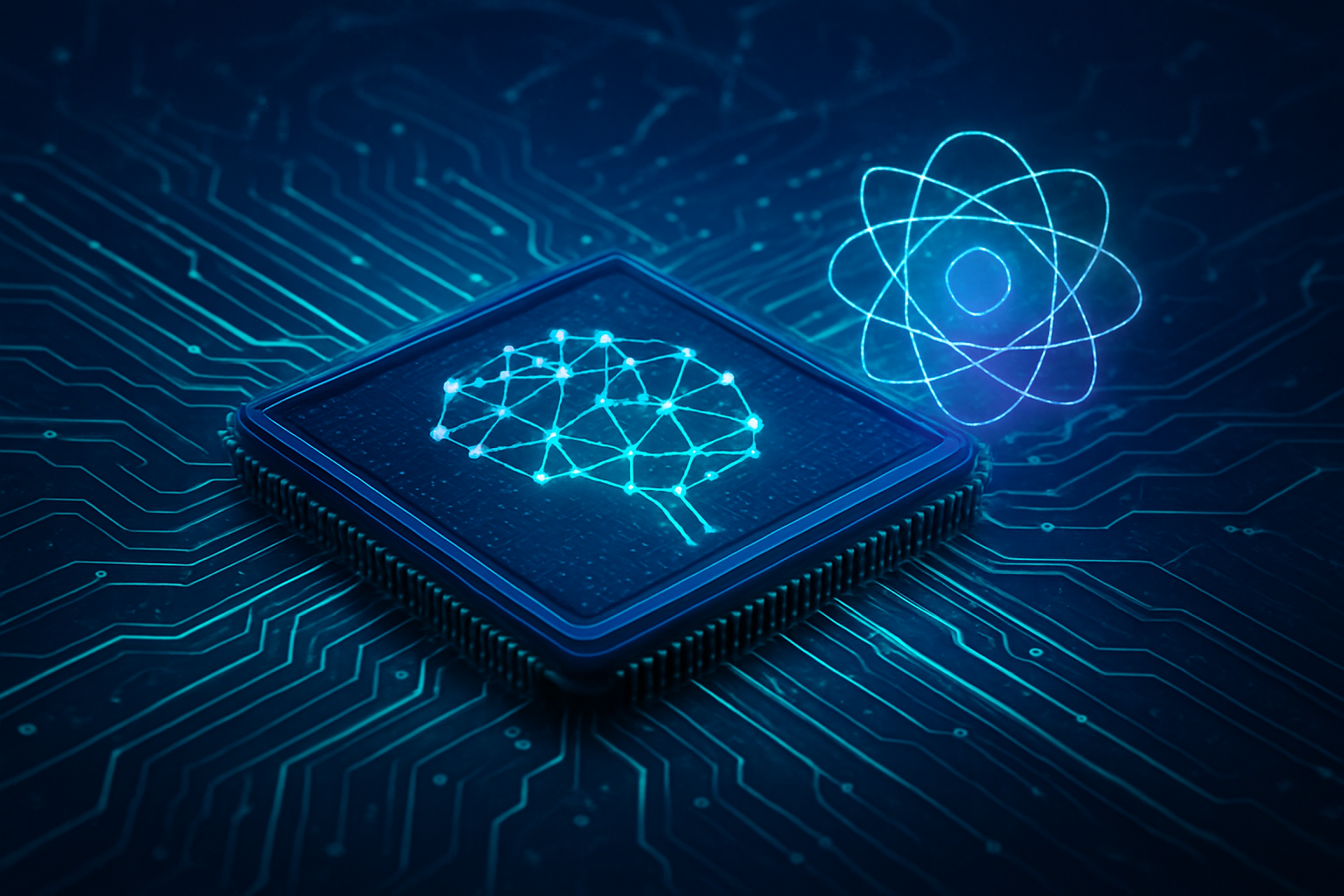
Tag: Semiconductors

  • Extreme Ultraviolet Lithography Market Set to Explode to $28.66 Billion by 2031, Fueling the Next Era of AI Chips

    Extreme Ultraviolet Lithography Market Set to Explode to $28.66 Billion by 2031, Fueling the Next Era of AI Chips

    The global Extreme Ultraviolet Lithography (EUL) market is on the cusp of unprecedented expansion, projected to reach a staggering $28.66 billion by 2031, exhibiting a robust Compound Annual Growth Rate (CAGR) of 22%. This explosive growth is not merely a financial milestone; it signifies a critical inflection point for the entire technology industry, particularly for advanced chip manufacturing. EUL is the foundational technology enabling the creation of the smaller, more powerful, and energy-efficient semiconductors that are indispensable for the next generation of artificial intelligence (AI), high-performance computing (HPC), 5G, and autonomous systems.

    This rapid market acceleration underscores the indispensable role of EUL in sustaining Moore's Law, pushing the boundaries of miniaturization, and providing the raw computational power required for the escalating demands of modern AI. As the world increasingly relies on sophisticated digital infrastructure and intelligent systems, the precision and capabilities offered by EUL are becoming non-negotiable, setting the stage for profound advancements across virtually every sector touched by computing.

    The Dawn of Sub-Nanometer Processing: How EUV is Redefining Chip Manufacturing

    Extreme Ultraviolet Lithography (EUL) represents a monumental leap in semiconductor fabrication, employing ultra-short wavelength light to etch incredibly intricate patterns onto silicon wafers. Unlike its predecessors, EUL utilizes light at a wavelength of approximately 13.5 nanometers (nm), a stark contrast to the 193 nm used in traditional Deep Ultraviolet (DUV) lithography. This significantly shorter wavelength is the key to EUL's superior resolution, enabling the production of features below 7 nm and paving the way for advanced process nodes such as 7nm, 5nm, 3nm, and even sub-2nm.

    The technical prowess of EUL systems is a marvel of modern engineering. The EUV light itself is generated by a laser-produced plasma (LPP) source, where high-power CO2 lasers fire at microscopic droplets of molten tin in a vacuum, creating an intensely hot plasma that emits EUV radiation. Because EUV light is absorbed by virtually all materials, the entire process must occur in a vacuum, and the optical system relies on a complex arrangement of highly specialized, ultra-smooth reflective mirrors. These mirrors, composed of alternating layers of molybdenum and silicon, are engineered to reflect 13.5 nm light with minimal loss. Photomasks, too, are reflective, differing from the transparent masks used in DUV, and are protected by thin, high-transmission pellicles. Current EUV systems (e.g., ASML's NXE series) operate with a 0.33 Numerical Aperture (NA), but the next generation, High-NA EUV, will increase this to 0.55 NA, promising even finer resolutions of 8 nm.

    This approach dramatically differs from previous methods, primarily DUV lithography. DUV systems use refractive lenses and operate in ambient air, relying heavily on complex and costly multi-patterning techniques (e.g., double or quadruple patterning) to achieve smaller feature sizes. These multi-step processes increase manufacturing complexity, defect rates, and overall costs. EUL, by contrast, enables single patterning for critical layers at advanced nodes, simplifying the manufacturing flow, reducing defectivity, and improving throughput. The initial reaction from the semiconductor industry has been one of immense investment and excitement, recognizing EUL as a "game-changer" and "essential" for sustaining Moore's Law. While the AI research community doesn't directly react to lithography as a field, they acknowledge EUL as a crucial enabling technology, providing the powerful chips necessary for their increasingly complex models. Intriguingly, AI and machine learning are now being integrated into EUV systems themselves, optimizing processes and enhancing efficiency.

    Corporate Titans and the EUV Arms Race: Shifting Power Dynamics in AI

    The proliferation of Extreme Ultraviolet Lithography is fundamentally reshaping the competitive landscape for AI companies, tech giants, and even startups, creating distinct advantages and potential disruptions. The ability to access and leverage EUL technology is becoming a strategic imperative, concentrating power among a select few industry leaders.

    Foremost among the beneficiaries is ASML Holding N.V. (NASDAQ: ASML), the undisputed monarch of the EUL market. As the world's sole producer of EUL machines, ASML's dominant position makes it indispensable for manufacturing cutting-edge chips. Its revenue is projected to grow significantly, fueled by AI-driven semiconductor demand and increasing EUL adoption. The rollout of High-NA EUL systems further solidifies ASML's long-term growth prospects, enabling breakthroughs in sub-2 nanometer transistor technologies. Following closely are the leading foundries and integrated device manufacturers (IDMs). Taiwan Semiconductor Manufacturing Company (NYSE: TSM), the largest pure-play foundry, heavily leverages EUL to produce advanced logic and memory chips for a vast array of tech companies. Their robust investments in global manufacturing capacity, driven by strong AI and HPC requirements, position them as a massive beneficiary. Similarly, Samsung Electronics Co., Ltd. (KRX: 005930) is a major producer and supplier that utilizes EUL to enhance its chip manufacturing capabilities, producing advanced processors and memory for its diverse product portfolio. Intel Corporation (NASDAQ: INTC) is also aggressively pursuing EUL, particularly High-NA EUL, to regain its leadership in chip manufacturing and produce 1.5nm and sub-1nm chips, crucial for its competitive positioning in the AI chip market.

    Chip designers like NVIDIA Corporation (NASDAQ: NVDA) and Advanced Micro Devices, Inc. (NASDAQ: AMD) are indirect but significant beneficiaries. While they don't manufacture EUL machines, their reliance on foundries like TSMC to produce their advanced AI GPUs and CPUs means that EUL-enabled fabrication directly translates to more powerful and efficient chips for their products. The demand for NVIDIA's AI accelerators, in particular, will continue to fuel the need for EUL-produced semiconductors. For tech giants operating vast cloud infrastructures and developing their own AI services, such as Alphabet Inc. (NASDAQ: GOOGL), Microsoft Corporation (NASDAQ: MSFT), and Amazon.com, Inc. (NASDAQ: AMZN), EUL-enabled chips power their data centers and AI offerings, allowing them to expand their market share as AI leaders. However, startups face considerable challenges due to the high operational costs and technical complexities of EUL, often needing to rely on tech giants for access to computing infrastructure. This dynamic could lead to increased consolidation and make it harder for smaller companies to compete on hardware innovation.

    The competitive implications are profound: EUL creates a significant divide. Companies with access to the most advanced EUL technology can produce superior chips, leading to increased performance for AI models, accelerated innovation cycles, and a centralization of resources among a few key players. This could disrupt existing products and services by making older hardware less competitive for demanding AI workloads and enabling entirely new categories of AI-powered devices. Strategically, EUL offers technology leadership, performance differentiation, long-term cost efficiency through higher yields, and enhanced supply chain resilience for those who master its complexities.

    Beyond the Wafer: EUV's Broad Impact on AI and the Global Tech Landscape

    Extreme Ultraviolet Lithography is not merely an incremental improvement in manufacturing; it is a foundational technology that underpins the current and future trajectory of Artificial Intelligence. By sustaining and extending Moore's Law, EUVL directly enables the exponential growth in computational capabilities that is the lifeblood of modern AI. Without EUVL, the relentless demand for more powerful, energy-efficient processors by large language models, deep neural networks, and autonomous systems would face insurmountable physical barriers, stifling innovation across the AI landscape.

    Its impact reverberates across numerous industries. In semiconductor manufacturing, EUVL is indispensable for producing the high-performance AI processors that drive global technological progress. Leading foundries and IDMs have fully integrated EUVL into their high-volume manufacturing lines for advanced process nodes, ensuring that companies at the forefront of AI development can produce more powerful, energy-efficient AI accelerators. For High-Performance Computing (HPC) and Data Centers, EUVL is critical for creating the advanced chips needed to power hyperscale data centers, which are the backbone of large language models and other data-intensive AI applications. Autonomous systems, such as self-driving cars and advanced robotics, directly benefit from the precision and power enabled by EUVL, allowing for faster and more efficient real-time decision-making. In consumer electronics, EUVL underpins the development of advanced AI features in smartphones, tablets, and IoT devices, enhancing user experiences. Even in medical and scientific research, EUVL-enabled chips facilitate breakthroughs in complex fields like drug discovery and climate modeling by providing unprecedented computational power.

    However, this transformative technology comes with significant concerns. The cost of EUL machines is extraordinary, with a single system costing hundreds of millions of dollars, and the latest High-NA models exceeding $370 million. Operational costs, including immense energy consumption (a single tool can rival the annual energy consumption of an entire city), further concentrate advanced chip manufacturing among a very few global players. The supply chain is also incredibly fragile, largely due to ASML's near-monopoly. Specialized components often come from single-source suppliers, making the entire ecosystem vulnerable to disruptions. Furthermore, EUL has become a potent factor in geopolitics, with export controls and technology restrictions, particularly those influenced by the United States on ASML's sales to China, highlighting EUVL as a "chokepoint" in global semiconductor manufacturing. This "techno-nationalism" can lead to market fragmentation and increased production costs.

    EUVL's significance in AI history can be likened to foundational breakthroughs such as the invention of the transistor or the development of the GPU. Just as these innovations enabled subsequent leaps in computing, EUVL provides the underlying hardware capability to manufacture the increasingly powerful processors required for AI. It has effectively extended the viability of Moore's Law, providing the hardware foundation necessary for the development of complex AI models. What makes this era unique is the emergent "AI supercycle," where AI and machine learning algorithms are also being integrated into EUVL systems themselves, optimizing fabrication processes and creating a powerful, self-improving technological feedback loop.

    The Road Ahead: Navigating the Future of Extreme Ultraviolet Lithography

    The future of Extreme Ultraviolet Lithography promises a relentless pursuit of miniaturization and efficiency, driven by the insatiable demands of AI and advanced computing. The coming years will witness several pivotal developments, pushing the boundaries of what's possible in chip manufacturing.

    In the near-term (present to 2028), the most significant advancement is the full introduction and deployment of High-NA EUV lithography. ASML (NASDAQ: ASML) has already shipped the first 0.55 NA scanner to Intel (NASDAQ: INTC), with high-volume manufacturing platforms expected to be operational by 2025. This leap in numerical aperture will enable even finer resolution patterns, crucial for sub-2nm nodes. Concurrently, there will be continued efforts to increase EUV light source power, enhancing wafer throughput, and to develop advanced photoresist materials and improved photomasks for higher precision and defect-free production. Looking further ahead (beyond 2028), research is already exploring Hyper-NA EUV with NAs of 0.75 or higher, and even shorter wavelengths, potentially below 5nm, to extend Moore's Law beyond 2030. Concepts like coherent light sources and Directed Self-Assembly (DSA) lithography are also on the horizon to further refine performance. Crucially, the integration of AI and machine learning into the entire EUV manufacturing process is expected to revolutionize optimization, predictive maintenance, and real-time adjustments.

    These advancements will unlock a new generation of applications and use cases. EUL will continue to drive the development of faster, more efficient, and powerful processors for Artificial Intelligence systems, including large language models and edge AI. It is essential for 5G and beyond telecommunications infrastructure, High-Performance Computing (HPC), and increasingly sophisticated autonomous systems. Furthermore, EUVL will play a vital role in advanced packaging technologies and 3D integration, allowing for greater levels of integration and miniaturization in chips. Despite the immense potential, significant challenges remain. High-NA EUV introduces complexities such as thinner photoresists leading to stochastic effects, reduced depth of focus, and enhanced mask 3D effects. Defectivity remains a persistent hurdle, requiring breakthroughs to achieve incredibly low defect rates for high-volume manufacturing. The cost of these machines and their immense operational energy consumption continue to be substantial barriers.

    Experts are unanimous in predicting substantial market growth for EUVL, reinforcing its role in extending Moore's Law and enabling chips at sub-2nm nodes. They foresee the continued dominance of foundries, driven by their focus on advanced-node manufacturing. Strategic investments from major players like TSMC (NYSE: TSM), Samsung (KRX: 005930), and Intel (NASDAQ: INTC), coupled with governmental support through initiatives like the U.S. CHIPS and Science Act, will accelerate EUV adoption. While EUV and High-NA EUV will drive advanced-node manufacturing, the industry will also need to watch for potential supply chain bottlenecks and the long-term viability of alternative lithography approaches being explored by various nations.

    EUV: A Cornerstone of the AI Revolution

    Extreme Ultraviolet Lithography stands as a testament to human ingenuity, a complex technological marvel that has become the indispensable backbone of the modern digital age. Its projected growth to $28.66 billion by 2031 with a 22% CAGR is not merely a market forecast; it is a clear indicator of its critical role in powering the ongoing AI revolution and shaping the future of technology. By enabling the production of smaller, more powerful, and energy-efficient chips, EUVL is directly responsible for the exponential leaps in computational capabilities that define today's advanced AI systems.

    The significance of EUL in AI history cannot be overstated. It has effectively "saved Moore's Law," providing the hardware foundation necessary for the development of complex AI models, from large language models to autonomous systems. Beyond its enabling role, EUVL systems are increasingly integrating AI themselves, creating a powerful feedback loop where advancements in AI drive the demand for sophisticated semiconductors, and these semiconductors, in turn, unlock new possibilities for AI. This symbiotic relationship ensures a continuous cycle of innovation, making EUVL a cornerstone of the AI era.

    Looking ahead, the long-term impact of EUVL will be profound and pervasive, driving sustained miniaturization, performance enhancement, and technological innovation across virtually every sector. It will facilitate the transition to even smaller process nodes, essential for next-generation consumer electronics, cloud computing, 5G, and emerging fields like quantum computing. However, the concentration of this critical technology in the hands of a single dominant supplier, ASML (NASDAQ: ASML), presents ongoing geopolitical and strategic challenges that will continue to shape global supply chains and international relations.

    In the coming weeks and months, industry observers should closely watch the full deployment and yield rates of High-NA EUV lithography systems by leading foundries, as these will be crucial indicators of their impact on future chip performance. Continued advancements in EUV components, particularly light sources and photoresist materials, will be vital for further enhancements. The increasing integration of AI and machine learning across the EUVL ecosystem, aimed at optimizing efficiency and precision, will also be a key trend. Finally, geopolitical developments, export controls, and government incentives will continue to influence regional fab expansions and the global competitive landscape, all of which will determine the pace and direction of the AI revolution powered by Extreme Ultraviolet Lithography.


    This content is intended for informational purposes only and represents analysis of current AI developments.

    TokenRing AI delivers enterprise-grade solutions for multi-agent AI workflow orchestration, AI-powered development tools, and seamless remote collaboration platforms.
    For more information, visit https://www.tokenring.ai/.

  • ChipAgents Secures $21 Million to Revolutionize AI Chip Design with Agentic AI Platform

    ChipAgents Secures $21 Million to Revolutionize AI Chip Design with Agentic AI Platform

    Santa Barbara, CA – October 22, 2025 – ChipAgents, a trailblazing electronic design automation (EDA) company, has announced the successful closure of an oversubscribed $21 million Series A funding round. This significant capital infusion, which brings their total funding to $24 million, is set to propel the development and deployment of its innovative agentic AI platform, designed to redefine the landscape of AI chip design and verification. The announcement, made yesterday, October 21, 2025, underscores a pivotal moment in the AI semiconductor sector, highlighting a growing investor confidence in AI-driven solutions for hardware development.

    The funding round signals a robust belief in ChipAgents' vision to automate and accelerate the notoriously complex and time-consuming process of chip design. With modern chips housing billions, even trillions, of logic gates, traditional manual methods are becoming increasingly untenable. ChipAgents' platform promises to alleviate this bottleneck, empowering engineers to focus on higher-level innovation rather than tedious, routine tasks, thereby ushering in a new era of efficiency and capability in semiconductor development.

    Unpacking the Agentic AI Revolution in Silicon Design

    ChipAgents' core innovation lies in its "agentic AI platform," a sophisticated system engineered to transform how hardware companies define, validate, and refine Register-Transfer Level (RTL) code. This platform leverages generative AI to automate a wide spectrum of routine design and verification tasks, offering a stark contrast to previous, predominantly manual, and often error-prone approaches.

    At its heart, the platform boasts several key functionalities. It intelligently automates the initial stages of chip design by generating RTL code and automatically producing comprehensive documentation, tasks that traditionally demand extensive human effort. Furthermore, it excels in identifying inconsistencies and flaws by cross-checking specifications across multiple documents, a critical step in preventing costly errors down the line. Perhaps most impressively, ChipAgents dramatically accelerates debugging and verification processes. It can automatically generate test benches, rules, and assertions in minutes – tasks that typically consume weeks of an engineer's time. This significant speed-up is achieved by empowering designers with natural language-based commands, allowing them to intuitively guide the AI in code generation, testbench creation, debugging, and verification. The company claims an ambitious goal of boosting RTL design and verification productivity by a factor of 10x, and has already demonstrated an 80% higher productivity in verification compared to industry standards across independent teams, with its platform currently deployed at 50 leading semiconductor companies.

    Initial reactions from the AI research community and industry experts have been overwhelmingly positive. Professor William Wang, founder and CEO of ChipAgents, emphasized that the semiconductor industry is "witnessing the transformation… into agentic AI solutions for design verification." Investors echoed this sentiment, with Lance Co Ting Keh, Venture Partner at Bessemer Venture Partners, hailing ChipAgents as "the best product in the market that does AI-powered RTL design, debugging, and verification for chip developers." He further noted that the platform "brings together disparate EDA tools from spec ingestion to waveform analysis," positioning it as a "true force multiplier for hardware design engineers." This unified approach and significant productivity gains mark a substantial departure from fragmented EDA toolchains and manual processes that have long characterized the industry.

    Reshaping the Competitive Landscape: Implications for Tech Giants and Startups

    The success of ChipAgents' Series A funding round and the rapid adoption of its platform carry significant implications for the broader AI and semiconductor industries. Semiconductor giants like Micron Technology Inc. (NASDAQ: MU), MediaTek Inc. (TPE: 2454), and Ericsson (NASDAQ: ERIC), who participated as strategic backers in the funding round, stand to benefit directly. Their investment signifies a commitment to integrating cutting-edge AI-driven design tools into their workflows, ultimately leading to faster, more efficient, and potentially more innovative chip development for their own products. The 50 leading semiconductor companies already deploying ChipAgents' technology further underscore this immediate benefit.

    For major AI labs and tech companies, this development means the promise of more powerful and specialized AI hardware arriving on the market at an accelerated pace. As AI models grow in complexity and demand increasingly tailored silicon, tools that can speed up custom chip design become invaluable. This could give companies leveraging ChipAgents' platform a competitive edge in developing next-generation AI accelerators and specialized processing units.

    The competitive landscape for established EDA tool providers like Synopsys Inc. (NASDAQ: SNPS), Cadence Design Systems Inc. (NASDAQ: CDNS), and Siemens EDA (formerly Mentor Graphics) could face significant disruption. While these incumbents offer comprehensive suites of tools, ChipAgents' agentic AI platform directly targets a core, labor-intensive segment of their market – RTL design and verification – with a promise of unprecedented automation and productivity. The fact that former CTOs and CEOs from these very companies (Raúl Camposano from Synopsys, Jack Harding from Cadence, Wally Rhines from Mentor Graphics) are now advisors to ChipAgents speaks volumes about the perceived transformative power of this new approach. ChipAgents is strategically positioned to capture a substantial share of the growing market for AI-powered EDA solutions, potentially forcing incumbents to rapidly innovate or acquire similar capabilities to remain competitive.

    Broader Significance: Fueling the AI Hardware Renaissance

    ChipAgents' breakthrough fits squarely into the broader AI landscape, addressing one of its most critical bottlenecks: the efficient design and production of specialized AI hardware. As AI models become larger and more complex, the demand for custom-designed chips optimized for specific AI workloads (e.g., neural network inference, training, specialized data processing) has skyrocketed. This funding round underscores a significant trend: the convergence of generative AI with core engineering disciplines, moving beyond mere software code generation to fundamental hardware design.

    The impacts are profound. By dramatically shortening chip design cycles and accelerating verification, ChipAgents directly contributes to the pace of AI innovation. Faster chip development means quicker iterations of AI hardware, enabling more powerful and efficient AI systems to reach the market sooner. This, in turn, fuels advancements across various AI applications, from autonomous vehicles and advanced robotics to sophisticated data analytics and scientific computing. The platform's ability to reduce manual effort could also lead to significant cost savings in development, making advanced chip design more accessible and potentially fostering a new wave of semiconductor startups.

    Potential concerns, though not immediately apparent, could include the long-term implications for the workforce, particularly for entry-level verification engineers whose tasks might be increasingly automated. There's also the ongoing challenge of ensuring the absolute reliability and security of AI-generated hardware designs, as flaws at this fundamental level could have catastrophic consequences. Nevertheless, this development can be compared to previous AI milestones, such as the application of AI to software code generation, but it takes it a step further by applying these powerful generative capabilities to the intricate world of silicon, pushing the boundaries of what AI can design autonomously.

    The Road Ahead: Future Developments and Expert Predictions

    Looking ahead, ChipAgents is poised for rapid expansion and deeper integration into the semiconductor ecosystem. In the near term, we can expect to see continued adoption of its platform by a wider array of semiconductor companies, driven by the compelling productivity gains demonstrated thus far. The company will likely focus on expanding the platform's capabilities, potentially encompassing more stages of the chip design flow beyond RTL, such as high-level synthesis or even physical design aspects, further solidifying its "agentic AI" approach.

    Long-term, the potential applications and use cases are vast. We could be on the cusp of an era where fully autonomous chip design, guided by high-level specifications, becomes a reality. This could lead to the creation of highly specialized, ultra-efficient AI chips tailored for niche applications, accelerating innovation in areas currently limited by hardware constraints. Imagine AI designing AI, creating a virtuous cycle of technological advancement.

    However, challenges remain. Ensuring the trustworthiness and verifiability of AI-generated RTL code will be paramount, requiring robust validation frameworks. Seamless integration into diverse and often legacy EDA toolchains will also be a continuous effort. Experts predict that AI-driven EDA tools like ChipAgents will become indispensable, further accelerating the pace of Moore's Law and enabling the development of increasingly complex and performant chips that would be impossible to design with traditional methods. The industry is watching to see how quickly these agentic AI solutions can mature and become the standard for semiconductor development.

    A New Dawn for Silicon Innovation

    ChipAgents' $21 million Series A funding marks a significant inflection point in the artificial intelligence and semiconductor industries. It underscores the critical role that specialized AI hardware plays in the broader AI revolution and highlights the transformative power of generative and agentic AI applied to complex engineering challenges. The company's platform, with its promise of 10x productivity gains and 80% higher verification efficiency, is not just an incremental improvement; it represents a fundamental shift in how chips will be designed.

    This development will undoubtedly be remembered as a key milestone in AI history, demonstrating how intelligent agents can fundamentally redefine human-computer interaction in highly technical fields. The long-term impact will likely be a dramatic acceleration in the development of AI hardware, leading to more powerful, efficient, and innovative AI systems across all sectors. In the coming weeks and months, industry observers will be watching closely for further adoption metrics, new feature announcements from ChipAgents, and how established EDA players respond to this formidable new competitor. The race to build the future of AI hardware just got a significant boost.


    This content is intended for informational purposes only and represents analysis of current AI developments.

    TokenRing AI delivers enterprise-grade solutions for multi-agent AI workflow orchestration, AI-powered development tools, and seamless remote collaboration platforms.
    For more information, visit https://www.tokenring.ai/.

  • TSMC: The Unseen Architect Powering the AI Revolution with Unprecedented Spending

    TSMC: The Unseen Architect Powering the AI Revolution with Unprecedented Spending

    Taipei, Taiwan – October 22, 2025 – Taiwan Semiconductor Manufacturing Company (TSMC) (NYSE: TSM) stands as the undisputed titan in the global semiconductor industry, a position that has become critically pronounced amidst the burgeoning artificial intelligence revolution. As the leading pure-play foundry, TSMC's advanced manufacturing capabilities are not merely facilitating but actively dictating the pace and scale of AI innovation worldwide. The company's relentless pursuit of cutting-edge process technologies, coupled with a staggering capital expenditure, underscores its indispensable role as the "backbone" and "arms supplier" to an AI industry experiencing insatiable demand.

    The immediate significance of TSMC's dominance cannot be overstated. With an estimated 90-92% market share in advanced AI chip manufacturing, virtually every major AI breakthrough, from sophisticated large language models (LLMs) to autonomous systems, relies on TSMC's silicon. This concentration of advanced manufacturing power in one entity highlights both the incredible efficiency and technological leadership of TSMC, as well as the inherent vulnerabilities within the global AI supply chain. As AI-related revenue continues to surge, TSMC's strategic investments and technological roadmap are charting the course for the next generation of intelligent machines and services.

    The Microscopic Engines: TSMC's Technical Prowess in AI Chip Manufacturing

    TSMC's technological leadership is rooted in its continuous innovation across advanced process nodes and sophisticated packaging solutions, which are paramount for the high-performance and power-efficient chips demanded by AI.

    At the forefront of miniaturization, TSMC's 3nm process (N3 family) has been in high-volume production since 2022, contributing 23% to its wafer revenue in Q3 2025. This node delivers a 1.6x increase in logic transistor density and a 25-30% reduction in power consumption compared to its 5nm predecessor. Major AI players like Apple (NASDAQ: AAPL), NVIDIA (NASDAQ: NVDA), and Advanced Micro Devices (NASDAQ: AMD) are already leveraging TSMC's 3nm technology. The monumental leap, however, comes with the 2nm process (N2), transitioning from FinFET to Gate-All-Around (GAA) nanosheet transistors. Set for mass production in the second half of 2025, N2 promises a 15% performance boost at the same power or a remarkable 25-30% power reduction compared to 3nm, along with a 1.15x increase in transistor density. This architectural shift is critical for future AI models, with an improved variant (N2P) scheduled for late 2026. Looking further ahead, TSMC's roadmap includes the A16 (1.6nm-class) process with "Super Power Rail" technology and the A14 (1.4nm) node, targeting mass production in late 2028, promising even greater performance and efficiency gains.

    Beyond traditional scaling, TSMC's advanced packaging technologies are equally indispensable for AI chips, effectively overcoming the "memory wall" bottleneck. CoWoS (Chip-on-Wafer-on-Substrate), TSMC's pioneering 2.5D advanced packaging technology, integrates multiple active silicon dies, such as logic SoCs (e.g., GPUs or AI accelerators) and High Bandwidth Memory (HBM) stacks, on a passive silicon interposer. This significantly reduces data travel distances, enabling massively increased bandwidth (up to 8.6 Tb/s) and lower latency—crucial for memory-bound AI workloads. TSMC is aggressively expanding its CoWoS capacity, aiming to quadruple output by the end of 2025 and reach 130,000 wafers per month by 2026. Furthermore, SoIC (System-on-Integrated-Chips), a 3D stacking technology planned for mass production in 2025, pushes boundaries further by facilitating ultra-high bandwidth density between stacked dies with ultra-fine pitches below 2 microns, providing lower latency and higher power efficiency. AMD's MI300, for instance, utilizes SoIC paired with CoWoS. These innovations differentiate TSMC by offering integrated, high-density, and high-bandwidth solutions that far surpass previous 2D packaging approaches.

    Initial reactions from the AI research community and industry experts have been overwhelmingly positive, hailing TSMC as the "indispensable architect" and "golden goose of AI." Experts view TSMC's 2nm node and advanced packaging as critical enablers for the next generation of AI models, including multimodal and foundation models. However, concerns persist regarding the extreme concentration of advanced AI chip manufacturing, which could lead to supply chain vulnerabilities and significant cost increases for next-generation chips, potentially up to 50% compared to 3nm.

    Market Reshaping: Impact on AI Companies, Tech Giants, and Startups

    TSMC's unparalleled dominance in advanced AI chip manufacturing is profoundly shaping the competitive landscape, conferring significant strategic advantages to its partners and creating substantial barriers to entry for others.

    Companies that stand to benefit are predominantly the leading innovators in AI and high-performance computing (HPC) chip design. NVIDIA (NASDAQ: NVDA), a cornerstone client, relies heavily on TSMC for its industry-leading GPUs like the H100, Blackwell, and future architectures, which are crucial for AI accelerators and data centers. Apple (NASDAQ: AAPL) secures a substantial portion of initial 2nm production capacity for its AI-powered M-series chips for Macs and iPhones. AMD (NASDAQ: AMD) leverages TSMC for its next-generation data center GPUs (MI300 series) and Ryzen processors, positioning itself as a strong challenger. Hyperscale cloud providers and tech giants such as Alphabet (NASDAQ: GOOGL) (Google), Amazon (NASDAQ: AMZN), Meta Platforms (NASDAQ: META), and Microsoft (NASDAQ: MSFT) are increasingly designing custom AI silicon, optimizing their vast AI infrastructures and maintaining market leadership through TSMC's manufacturing prowess. Even Tesla (NASDAQ: TSLA) relies on TSMC for its AI-powered self-driving chips.

    The competitive implications for major AI labs and tech companies are significant. TSMC's technological lead and capacity expansion further entrench the market leadership of companies with early access to cutting-edge nodes, establishing high barriers to entry for newer firms. While competitors like Samsung Electronics (KRX: 005930) and Intel (NASDAQ: INTC) are aggressively pursuing advanced nodes (e.g., Intel's 18A process, comparable to TSMC's 2nm, scheduled for mass production in H2 2025), TSMC generally maintains superior yield rates and established customer trust, making rapid migration unlikely due to massive technical risks and financial costs. The reliance on TSMC also encourages some tech giants to invest more heavily in their own chip design capabilities to gain greater control, though they remain dependent on TSMC for manufacturing.

    Potential disruption to existing products or services is multifaceted. The rapid advancement in AI chip technology, driven by TSMC's nodes, accelerates hardware obsolescence, compelling continuous upgrades to AI infrastructure. Conversely, TSMC's manufacturing capabilities directly accelerate the time-to-market for AI-powered products and services, potentially disrupting industries slower to adopt AI. The unprecedented performance and power efficiency leaps from 2nm technology are critical for enabling AI capabilities to migrate from energy-intensive cloud data centers to edge devices and consumer electronics, potentially triggering a major PC refresh cycle as generative AI transforms applications in smartphones, PCs, and autonomous vehicles. However, the immense R&D and capital expenditures associated with advanced nodes could lead to a significant increase in chip prices, potentially up to 50% compared to 3nm, which may be passed on to end-users and increase costs for AI infrastructure.

    TSMC's market positioning and strategic advantages are virtually unassailable. As of October 2025, it holds an estimated 70-71% market share in the global pure-play wafer foundry market. Its technological leadership in process nodes (3nm in high-volume production, 2nm mass production in H2 2025, A16 by 2026) and advanced packaging (CoWoS, SoIC) provides unmatched performance and energy efficiency. TSMC's pure-play foundry model fosters strong, long-term partnerships without internal competition, creating customer lock-in and pricing power, with prices expected to increase by 5-10% in 2025. Furthermore, TSMC is aggressively expanding its manufacturing footprint with a capital expenditure of $40-$42 billion in 2025, including new fabs in Arizona (U.S.) and Japan, and exploring Germany. This geographical diversification serves as a critical geopolitical hedge, reducing reliance on Taiwan-centric manufacturing in the face of U.S.-China tensions.

    The Broader Canvas: Wider Significance in the AI Landscape

    TSMC's foundational role extends far beyond mere manufacturing; it is fundamentally shaping the broader AI landscape, enabling unprecedented innovation while simultaneously highlighting critical geopolitical and supply chain vulnerabilities.

    TSMC's leading role in AI chip manufacturing and its substantial capital expenditures are not just business metrics but critical drivers for the entire AI ecosystem. The company's continuous innovation in process nodes (3nm, 2nm, A16, A14) and advanced packaging (CoWoS, SoIC) directly translates into the ability to create smaller, faster, and more energy-efficient chips. This capability is the linchpin for the next generation of AI breakthroughs, from sophisticated large language models and generative AI to complex autonomous systems. AI and high-performance computing (HPC) now account for a substantial portion of TSMC's revenue, exceeding 60% in Q3 2025, with AI-related revenue projected to double in 2025 and achieve a compound annual growth rate (CAGR) exceeding 45% through 2029. This symbiotic relationship where AI innovation drives demand for TSMC's chips, and TSMC's capabilities, in turn, enable further AI development, underscores its central role in the current "AI supercycle."

    The broader impacts are profound. TSMC's technology dictates who can build the most powerful AI systems, influencing the competitive landscape and acting as a powerful economic catalyst. The global AI chip market is projected to contribute over $15 trillion to the global economy by 2030. However, this rapid advancement also accelerates hardware obsolescence, compelling continuous upgrades to AI infrastructure. While AI chips are energy-intensive, TSMC's focus on improving power efficiency with new nodes directly influences the sustainability and scalability of AI solutions, even leveraging AI itself to design more energy-efficient chips.

    However, this critical reliance on TSMC also introduces significant potential concerns. The extreme supply chain concentration means any disruption to TSMC's operations could have far-reaching impacts across the global tech industry. More critically, TSMC's headquarters in Taiwan introduce substantial geopolitical risks. The island's strategic importance in advanced chip manufacturing has given rise to the concept of a "silicon shield," suggesting it acts as a deterrent against potential aggression, particularly from China. The ongoing "chip war" between the U.S. and China, characterized by U.S. export controls, directly impacts China's access to TSMC's advanced nodes and slows its AI development. To mitigate these risks, TSMC is aggressively diversifying its manufacturing footprint with multi-billion dollar investments in new fabrication plants in Arizona (U.S.), Japan, and potentially Germany. The company's near-monopoly also grants it pricing power, which can impact the cost of AI development and deployment.

    In comparison to previous AI milestones and breakthroughs, TSMC's contribution is unique in its emphasis on the physical hardware foundation. While earlier AI advancements were often centered on algorithmic and software innovations, the current era is fundamentally hardware-driven. TSMC's pioneering of the "pure-play" foundry business model in 1987 fundamentally reshaped the semiconductor industry, enabling fabless companies to innovate at an unprecedented pace. This model directly fueled the rise of modern computing and subsequently, AI, by providing the "picks and shovels" for the digital gold rush, much like how foundational technologies or companies enabled earlier tech revolutions.

    The Horizon: Future Developments in TSMC's AI Chip Manufacturing

    Looking ahead, TSMC is poised for continued groundbreaking developments, driven by the relentless demand for AI, though it must navigate significant challenges to maintain its trajectory.

    In the near-term and long-term, process technology advancements will remain paramount. The mass production of the 2nm (N2) process in the second half of 2025, featuring GAA nanosheet transistors, will be a critical milestone, enabling substantial improvements in power consumption and speed for next-generation AI accelerators from leading companies like NVIDIA, AMD, and Apple. Beyond 2nm, TSMC plans to introduce the A16 (1.6nm-class) and A14 (1.4nm) processes, with groundbreaking for the A14 facility in Taichung, Taiwan, scheduled for November 2025, targeting mass production by late 2028. These future nodes will offer even greater performance at lower power. Alongside process technology, advanced packaging innovations will be crucial. TSMC is aggressively expanding its CoWoS capacity, aiming to quadruple output by the end of 2025 and reach 130,000 wafers per month by 2026. Its 3D stacking technology, SoIC, is also slated for mass production in 2025, further boosting bandwidth density. TSMC is also exploring new square substrate packaging methods to embed more semiconductors per chip, targeting small volumes by 2027.

    These advancements will unlock a wide array of potential applications and use cases. They will continue to fuel the capabilities of AI accelerators and data centers for training massive LLMs and generative AI. More sophisticated autonomous systems, from vehicles to robotics, will benefit from enhanced edge AI. Smart devices will gain advanced AI capabilities, potentially triggering a major refresh cycle for smartphones and PCs. High-Performance Computing (HPC), augmented and virtual reality (AR/VR), and highly nuanced personal AI assistants are also on the horizon. TSMC is even leveraging AI in its own chip design, aiming for a 10-fold improvement in AI computing chip efficiency by using AI-powered design tools, showcasing a recursive innovation loop.

    However, several challenges need to be addressed. The exponential increase in power consumption by AI chips poses a major challenge. TSMC's electricity usage is projected to triple by 2030, making energy consumption a strategic bottleneck in the global AI race. The escalating cost of building and equipping modern fabs, coupled with immense R&D, means 2nm chips could see a price increase of up to 50% compared to 3nm, and overseas production in places like Arizona is significantly more expensive. Geopolitical stability remains the largest overhang, given the concentration of advanced manufacturing in Taiwan amidst US-China tensions. Taiwan's reliance on imported energy further underscores this fragility. TSMC's global diversification efforts are partly aimed at mitigating these risks, alongside addressing persistent capacity bottlenecks in advanced packaging.

    Experts predict that TSMC will remain an "indispensable architect" of the AI supercycle. AI is projected to drive double-digit growth in semiconductor demand through 2030, with the global AI chip market exceeding $150 billion in 2025. TSMC has raised its 2025 revenue growth forecast to the mid-30% range, with AI-related revenue expected to double in 2025 and achieve a CAGR exceeding 45% through 2029. By 2030, AI chips are predicted to constitute over 25% of TSMC's total revenue. 2025 is seen as a pivotal year where AI becomes embedded into the entire fabric of human systems, leading to the rise of "agentic AI" and multimodal AI.

    The AI Supercycle's Foundation: A Comprehensive Wrap-up

    TSMC has cemented its position as the undisputed leader in AI chip manufacturing, serving as the foundational backbone for the global artificial intelligence industry. Its unparalleled technological prowess, strategic business model, and massive manufacturing scale make it an indispensable partner for virtually every major AI innovator, driving the current "AI supercycle."

    The key takeaways are clear: TSMC's continuous innovation in process nodes (3nm, 2nm, A16) and advanced packaging (CoWoS, SoIC) is a technological imperative for AI advancement. The global AI industry is heavily reliant on this single company for its most critical hardware components, with AI now the primary growth engine for TSMC's revenue and capital expenditures. In response to geopolitical risks and supply chain vulnerabilities, TSMC is strategically diversifying its manufacturing footprint beyond Taiwan to locations like Arizona, Japan, and potentially Germany.

    TSMC's significance in AI history is profound. It is the "backbone" and "unseen architect" of the AI revolution, enabling the creation and scaling of advanced AI models by consistently providing more powerful, energy-efficient, and compact chips. Its pioneering of the "pure-play" foundry model fundamentally reshaped the semiconductor industry, directly fueling the rise of modern computing and subsequently, AI.

    In the long term, TSMC's dominance is poised to continue, driven by the structural demand for advanced computing. AI chips are expected to constitute a significant and growing portion of TSMC's total revenue, potentially reaching 50% by 2029. However, this critical position is tempered by challenges such as geopolitical tensions concerning Taiwan, the escalating costs of advanced manufacturing, and the need to address increasing power consumption.

    In the coming weeks and months, several key developments bear watching: the successful high-volume production ramp-up of TSMC's 2nm process node in the second half of 2025 will be a critical indicator of its continued technological leadership and ability to meet the "insatiable" demand from its 15 secured customers, many of whom are in the HPC and AI sectors. Updates on its aggressive expansion of CoWoS capacity, particularly its goal to quadruple output by the end of 2025, will directly impact the supply of high-end AI accelerators. Progress on the acceleration of advanced process node deployment at its Arizona fabs and developments in its other international sites in Japan and Germany will be crucial for supply chain resilience. Finally, TSMC's Q4 2025 earnings calls will offer further insights into the strength of AI demand, updated revenue forecasts, and capital expenditure plans, all of which will continue to shape the trajectory of the global AI landscape.


    This content is intended for informational purposes only and represents analysis of current AI developments.

    TokenRing AI delivers enterprise-grade solutions for multi-agent AI workflow orchestration, AI-powered development tools, and seamless remote collaboration platforms.
    For more information, visit https://www.tokenring.ai/.

  • Broadcom’s AI Ascendancy: A 66% Revenue Surge Propels Semiconductor Sector into a New Era

    Broadcom’s AI Ascendancy: A 66% Revenue Surge Propels Semiconductor Sector into a New Era

    SAN JOSE, CA – October 22, 2025 – Broadcom Inc. (NASDAQ: AVGO) is poised to cement its position as a foundational architect of the artificial intelligence revolution, projecting a staggering 66% year-over-year rise in AI revenues for its fourth fiscal quarter of 2025, reaching approximately $6.2 billion. This remarkable growth is expected to drive an overall 30% climb in its semiconductor sales, totaling around $10.7 billion for the same period. These bullish forecasts, unveiled by CEO Hock Tan during the company's Q3 fiscal 2025 earnings call on September 4, 2025, underscore the profound and accelerating link between advanced AI development and the demand for specialized semiconductor hardware.

    The anticipated financial performance highlights Broadcom's strategic pivot and robust execution in delivering high-performance, custom AI accelerators and cutting-edge networking solutions crucial for hyperscale AI data centers. As the AI "supercycle" intensifies, the company's ability to cater to the bespoke needs of tech giants and leading AI labs is translating directly into unprecedented revenue streams, signaling a fundamental shift in the AI hardware landscape. The figures underscore not just Broadcom's success, but the insatiable demand for the underlying silicon infrastructure powering the next generation of intelligent systems.

    The Technical Backbone of AI: Broadcom's Custom Silicon and Networking Prowess

    Broadcom's projected growth is rooted deeply in its sophisticated portfolio of AI-related semiconductor products and technologies. At the forefront are its custom AI accelerators, known as XPUs (Application-Specific Integrated Circuits or ASICs), which are co-designed with hyperscale clients to optimize performance for specific AI workloads. Unlike general-purpose GPUs (Graphics Processing Units) that serve a broad range of computational tasks, Broadcom's XPUs are meticulously tailored, offering superior performance-per-watt and cost efficiency for large-scale AI training and inference. This approach has allowed Broadcom to secure a commanding 75% market share in the custom ASIC AI accelerator market, with key partnerships including Google (co-developing TPUs for over a decade), Meta Platforms (NASDAQ: META), and a significant, widely reported $10 billion deal with OpenAI for custom AI chips and network systems. Broadcom plans to introduce next-generation XPUs built on advanced 3-nanometer technology in late fiscal 2025, further pushing the boundaries of efficiency and power.

    Complementing its custom silicon, Broadcom's advanced networking solutions are critical for linking the vast arrays of AI accelerators in modern data centers. The recently launched Tomahawk 6 – Davisson Co-Packaged Optics (CPO) Ethernet switch delivers an unprecedented 102.4 Terabits per second (Tbps) of optically enabled switching capacity in a single chip, doubling the bandwidth of its predecessor. This leap significantly alleviates network bottlenecks in demanding AI workloads, incorporating "Cognitive Routing 2.0" for dynamic congestion control and rapid failure detection, ensuring optimal utilization and reduced latency. Furthermore, its co-packaged optics design slashes power consumption per bit by up to 40%. Broadcom also introduced the Thor Ultra 800G AI Ethernet Network Interface Card (NIC), the industry's first, designed to interconnect hundreds of thousands of XPUs. Adhering to the open Ultra Ethernet Consortium (UEC) specification, Thor Ultra modernizes RDMA (Remote Direct Memory Access) with innovations like packet-level multipathing and selective retransmission, enabling unparalleled performance and efficiency in an open ecosystem.

    The technical community and industry experts have largely welcomed Broadcom's strategic direction. Analysts view Broadcom as a formidable competitor to Nvidia (NASDAQ: NVDA), particularly in the AI networking space and for custom AI accelerators. The focus on custom ASICs addresses the growing need among hyperscalers for greater control over their AI hardware stack, reducing reliance on off-the-shelf solutions. The immense bandwidth capabilities of Tomahawk 6 and Thor Ultra are hailed as "game-changers" for AI networking, enabling the creation of massive computing clusters with over a million XPUs. Broadcom's commitment to open, standards-based Ethernet solutions is seen as a crucial counterpoint to proprietary interconnects, offering greater flexibility and interoperability, and positioning the company as a long-term bullish catalyst in the AI infrastructure build-out.

    Reshaping the AI Competitive Landscape: Broadcom's Strategic Advantage

    Broadcom's surging AI and semiconductor growth has profound implications for the competitive landscape, benefiting several key players while intensifying pressure on others. Directly, Broadcom Inc. (NASDAQ: AVGO) stands to gain significantly from the escalating demand for its specialized silicon and networking products, solidifying its position as a critical infrastructure provider. Hyperscale cloud providers and AI labs such as Google (NASDAQ: GOOGL), Meta Platforms (NASDAQ: META), ByteDance, and OpenAI are major beneficiaries, leveraging Broadcom's custom AI accelerators to optimize their unique AI workloads, reduce vendor dependence, and achieve superior cost and energy efficiency for their vast data centers. Taiwan Semiconductor Manufacturing Company (NYSE: TSM), as a primary foundry for Broadcom, also stands to gain from the increased demand for advanced chip production and packaging. Furthermore, providers of High-Bandwidth Memory (HBM) like SK Hynix and Micron Technology (NASDAQ: MU), along with cooling and power management solution providers, will see boosted demand driven by the complexity and power requirements of these advanced AI chips.

    The competitive implications are particularly acute for established players in the AI chip market. Broadcom's aggressive push into custom ASICs and advanced Ethernet networking directly challenges Nvidia's long-standing dominance in general-purpose GPUs and its proprietary NVLink interconnect. While Nvidia is likely to retain leadership in highly demanding AI training scenarios, Broadcom's custom ASICs are gaining significant traction in large-scale inference and specialized AI applications due to their efficiency. OpenAI's multi-year collaboration with Broadcom for custom AI accelerators is a strategic move to diversify its supply chain and reduce its dependence on Nvidia. Similarly, Broadcom's success poses a direct threat to Advanced Micro Devices (NASDAQ: AMD) efforts to expand its market share in AI accelerators, especially in hyperscale data centers. The shift towards custom silicon could also put pressure on companies historically focused on general-purpose CPUs for data centers, like Intel (NASDAQ: INTC).

    This dynamic introduces significant disruption to existing products and services. The market is witnessing a clear shift from a sole reliance on general-purpose GPUs to a more heterogeneous mix of AI accelerators, with custom ASICs offering superior performance and energy efficiency for specific AI workloads, particularly inference. Broadcom's advanced networking solutions, such as Tomahawk 6 and Thor Ultra, are crucial for linking vast AI clusters and represent a direct challenge to proprietary interconnects, enabling higher speeds, lower latency, and greater scalability that fundamentally alter AI data center design. Broadcom's strategic advantages lie in its leadership in custom AI silicon, securing multi-year collaborations with leading tech giants, its dominant market position in Ethernet switching chips for cloud data centers, and its offering of end-to-end solutions that span both semiconductor and infrastructure software.

    Broadcom's Role in the AI Supercycle: A Broader Perspective

    Broadcom's projected growth is more than just a company success story; it's a powerful indicator of several overarching trends defining the current AI landscape. First, it underscores the explosive and seemingly insatiable demand for specialized AI infrastructure. The AI sector is in the midst of an "AI supercycle," characterized by massive, sustained investments in the computing backbone necessary to train and deploy increasingly complex models. Global semiconductor sales are projected to reach $1 trillion by 2030, with AI and cloud computing as primary catalysts, and Broadcom is clearly riding this wave.

    Second, Broadcom's prominence highlights the undeniable rise of custom silicon (ASICs or XPUs) as the next frontier in AI hardware. As AI models grow to trillions of parameters, general-purpose GPUs, while still vital, are increasingly being complemented or even supplanted by purpose-built ASICs. Companies like OpenAI are opting for custom silicon to achieve optimal performance, lower power consumption, and greater control over their AI stacks, allowing them to embed model-specific learning directly into the hardware for new levels of capability and efficiency. This shift, enabled by Broadcom's expertise, fundamentally impacts AI development by providing highly optimized, cost-effective, and energy-efficient processing power, accelerating innovation and enabling new AI capabilities.

    However, this rapid evolution also brings potential concerns. The heavy reliance on a few advanced semiconductor manufacturers for cutting-edge nodes and advanced packaging creates supply chain vulnerabilities, exacerbated by geopolitical tensions. While Broadcom is emerging as a strong competitor, the economic profit in the AI semiconductor industry remains highly concentrated among a few dominant players, raising questions about market concentration and potential long-term impacts on pricing and innovation. Furthermore, the push towards custom silicon, while offering performance benefits, can also lead to proprietary ecosystems and vendor lock-in.

    Comparing this era to previous AI milestones, Broadcom's role in the custom silicon boom is akin to the advent of GPUs in the late 1990s and early 2000s. Just as GPUs, particularly with Nvidia's CUDA, enabled the parallel processing crucial for the rise of deep learning and neural networks, custom ASICs are now unlocking the next level of performance and efficiency required for today's massive generative AI models. This "supercycle" is characterized by a relentless pursuit of greater efficiency and performance, directly embedding AI knowledge into hardware design. While Broadcom's custom XPUs are proprietary, the company's commitment to open standards in networking with its Ethernet solutions provides flexibility, allowing customers to build tailored AI architectures by mixing and matching components. This mixed approach aims to leverage the best of both worlds: highly optimized, purpose-built hardware coupled with flexible, standards-based connectivity for massive AI deployments.

    The Horizon: Future Developments and Challenges in Broadcom's AI Journey

    Looking ahead, Broadcom's trajectory in AI and semiconductors promises continued innovation and expansion. In the near-term (next 12-24 months), the multi-year collaboration with OpenAI, announced in October 2025, will see the co-development and deployment of 10 gigawatts of OpenAI-designed custom AI accelerators and networking systems, with rollouts beginning in mid-2026 and extending through 2029. This landmark partnership, potentially worth up to $200 billion in incremental revenue for Broadcom through 2029, will embed OpenAI's frontier model insights directly into the hardware. Broadcom will also continue advancing its custom XPUs, including the upcoming Google TPU v7 roadmap, and rolling out next-generation 3-nanometer XPUs in late fiscal 2025. Its advanced networking solutions, such as the Jericho3-AI and Ramon3 fabric chip, are expected to qualify for production, aiming for at least 10% shorter job completion times for AI accelerators. Furthermore, Broadcom's Wi-Fi 8 silicon solutions will extend AI capabilities to the broadband wireless edge, enabling AI-driven network optimization and enhanced security.

    Longer-term, Broadcom is expected to maintain its leadership in custom AI chips, with analysts predicting it could capture over $60 billion in annual AI revenue by 2030, assuming it sustains its dominant market share. The AI infrastructure expansion fueled by partnerships like OpenAI will see tighter integration and control over hardware by AI companies. Broadcom is also transitioning into a more balanced hardware-software provider, with the successful integration of VMware (NASDAQ: VMW) bolstering its recurring revenue streams. These advancements will enable a wide array of applications, from powering hyperscale AI data centers for generative AI and large language models to enabling localized intelligence in IoT devices and automotive systems through Edge AI. Broadcom's infrastructure software, enhanced by AI and machine learning, will also drive AIOps solutions for more intelligent IT operations.

    However, this rapid growth is not without its challenges. The immense power consumption and heat generation of next-generation AI accelerators necessitate sophisticated liquid cooling systems and ever more energy-efficient chip architectures. Broadcom is addressing this through power-efficient custom ASICs and CPO solutions. Supply chain resilience remains a critical concern, particularly for advanced packaging, with geopolitical tensions driving a restructuring of the semiconductor supply chain. Broadcom is collaborating with TSMC for advanced packaging and processes, including 3.5D packaging for its XPUs. Fierce competition from Nvidia, AMD, and Intel, alongside the increasing trend of hyperscale customers developing in-house chips, could also impact future revenue. While Broadcom differentiates itself with custom silicon and open, Ethernet-based networking, Nvidia's CUDA software ecosystem remains a dominant force, presenting a continuous challenge.

    Despite these hurdles, experts are largely bullish on Broadcom's future. It is widely seen as a "strong second player" after Nvidia in the AI chip market, with some analysts even predicting it could outperform Nvidia in 2026. Broadcom's strategic partnerships and focus on custom silicon are positioning it as an "indispensable force" in AI supercomputing infrastructure. Analysts project AI semiconductor revenue to reach $6.2 billion in Q4 2025 and potentially surpass $10 billion annually by 2026, with overall revenue expected to increase over 21% for the current fiscal year. The consensus is that tech giants will significantly increase AI spending, with the overall AI and data center hardware and software market expanding at 40-55% annually towards $1.4 trillion by 2027, ensuring a continued "arms race" in AI infrastructure where custom silicon will play an increasingly central role.

    A New Epoch in AI Hardware: Broadcom's Defining Moment

    Broadcom's projected 66% year-over-year surge in AI revenues and 30% climb in semiconductor sales for Q4 fiscal 2025 mark a pivotal moment in the history of artificial intelligence. The key takeaway is Broadcom's emergence as an indispensable architect of the modern AI infrastructure, driven by its leadership in custom AI accelerators (XPUs) and high-performance, open-standard networking solutions. This performance not only validates Broadcom's strategic focus but also underscores a fundamental shift in how the world's largest AI developers are building their computational foundations. The move towards highly optimized, custom silicon, coupled with ultra-fast, efficient networking, is shaping the next generation of AI capabilities.

    This development's significance in AI history cannot be overstated. It represents the maturation of the AI hardware ecosystem beyond general-purpose GPUs, entering an era where specialized, co-designed silicon is becoming paramount for achieving unprecedented scale, efficiency, and cost-effectiveness for frontier AI models. Broadcom is not merely supplying components; it is actively co-creating the very infrastructure that will define the capabilities of future AI. Its partnerships, particularly with OpenAI, are testament to this, enabling AI labs to embed their deep learning insights directly into the hardware, unlocking new levels of performance and control.

    As we look to the long-term impact, Broadcom's trajectory suggests an acceleration of AI development, fostering innovation by providing the underlying horsepower needed for more complex models and broader applications. The company's commitment to open Ethernet standards also offers a crucial alternative to proprietary ecosystems, potentially fostering greater interoperability and competition in the long run.

    In the coming weeks and months, the tech world will be watching for several key developments. The actual Q4 fiscal 2025 earnings report, expected soon, will confirm these impressive projections. Beyond that, the progress of the OpenAI custom accelerator deployments, the rollout of Broadcom's 3-nanometer XPUs, and the competitive responses from other semiconductor giants like Nvidia and AMD will be critical indicators of the evolving AI hardware landscape. Broadcom's current momentum positions it not just as a beneficiary, but as a defining force in the AI supercycle, laying the groundwork for an intelligent future.


    This content is intended for informational purposes only and represents analysis of current AI developments.

    TokenRing AI delivers enterprise-grade solutions for multi-agent AI workflow orchestration, AI-powered development tools, and seamless remote collaboration platforms.
    For more information, visit https://www.tokenring.ai/.

  • Rigaku Establishes Taiwan Technology Hub: A Strategic Leap for Semiconductor and AI Infrastructure

    Rigaku Establishes Taiwan Technology Hub: A Strategic Leap for Semiconductor and AI Infrastructure

    Rigaku Holdings Corporation (TSE: 6725) has announced a significant strategic expansion with the establishment of Rigaku Technology Taiwan Co., Ltd. (RTTW) and its integral Rigaku Technology Center Taiwan (RTC-TW). This pivotal move, with RTC-TW commencing full-scale operations in October 2025, underscores Rigaku's deep commitment to bolstering the critical semiconductor, life sciences, and materials science ecosystems within Taiwan. The new entity, taking over from the previously established Rigaku Taiwan Branch (RCTW), is poised to become a central hub for advanced research, development, and customer collaboration, signaling a substantial investment in the region's technological infrastructure and its burgeoning role in global innovation.

    This expansion is not merely an organizational restructuring but a calculated maneuver to embed Rigaku more deeply within one of the world's most dynamic technology landscapes. By establishing a robust local presence equipped with state-of-the-art facilities, Rigaku aims to accelerate technological advancements, enhance direct support for its strategic partners, and contribute to the sustainable growth of Taiwan's high-tech industries. The timing of this announcement, coinciding with the rapid global acceleration in AI and advanced computing, positions Rigaku to play an even more critical role in the foundational technologies that power these transformative fields.

    Technical Prowess and Strategic Alignment in Taiwan's Tech Heartland

    The core of Rigaku's (TSE: 6725) enhanced presence in Taiwan is the Rigaku Technology Center Taiwan (RTC-TW), envisioned as a cutting-edge engineering hub. This center is meticulously designed to foster advanced R&D, provide unparalleled customer support, and drive joint development initiatives with local partners. Equipped with sophisticated demonstration facilities and state-of-the-art laboratories, RTC-TW is set to significantly reduce development cycles and improve response times for customers in Taiwan's fast-paced technological environment.

    A key differentiator of RTC-TW is its integrated clean room, which meticulously replicates actual production environments. This facility, alongside dedicated spaces for product and technology demonstrations, comprehensive training, and collaborative development, is crucial for enhancing local engineering support. It allows Rigaku's technical teams to work in direct proximity to Taiwan's advanced semiconductor ecosystem, facilitating seamless integration and innovation while maintaining strong links to Rigaku's global R&D and manufacturing operations in Japan. The focus extends to critical measurements for thickness, composition, and crystallinity using advanced techniques like total reflection X-ray fluorescence (TXRF), X-ray topography, critical dimension measurement, stress/distortion analysis, and package inspection, all vital for next-generation logic and advanced packaging technologies.

    Beyond semiconductors, RTTW will also channel its expertise into materials science, offering solutions for evaluating material characteristics through X-ray diffraction (XRD), X-ray fluorescence (XRF), and 3D computed tomography (3DCT) imaging. The life sciences sector will also benefit from Rigaku's presence, with services such as biomolecular structure analysis and support for drug development. This comprehensive approach ensures that RTTW addresses a broad spectrum of scientific and industrial needs, differentiating itself by providing integrated analytical solutions crucial for the precision and innovation demanded by modern technological advancements, particularly those underpinning AI hardware and research.

    Implications for the AI and Tech Industry Ecosystem

    Rigaku's (TSE: 6725) strategic investment in Taiwan, particularly its focus on advanced semiconductor measurement and materials science, carries significant implications for AI companies, tech giants, and startups alike. Companies heavily reliant on cutting-edge semiconductor manufacturing, such as NVIDIA (NASDAQ: NVDA), AMD (NASDAQ: AMD), and Intel (NASDAQ: INTC), along with major foundries like Taiwan Semiconductor Manufacturing Company (TSMC) (NYSE: TSM), stand to directly benefit. Rigaku's enhanced local presence means quicker access to advanced metrology and inspection tools, crucial for optimizing the production of high-performance AI chips and advanced packaging, which are the backbone of modern AI infrastructure.

    The competitive landscape for major AI labs and tech companies will be subtly but significantly impacted. As the demand for more powerful and efficient AI hardware escalates, the precision and quality of semiconductor components become paramount. Rigaku's ability to provide localized, high-fidelity measurement and analysis tools directly to Taiwanese fabs can accelerate the development and deployment of next-generation AI accelerators. This could indirectly give companies utilizing these advanced fabs a competitive edge in bringing more capable AI solutions to market faster.

    Potential disruption to existing products or services might arise from the accelerated pace of innovation enabled by Rigaku's closer collaboration with Taiwanese manufacturers. Companies that previously relied on less sophisticated or slower analytical processes might find themselves needing to upgrade to maintain competitive quality and throughput. For startups in AI hardware or advanced materials, having a cutting-edge analytical partner like Rigaku in close proximity could lower barriers to innovation, allowing them to rapidly prototype and test new designs with confidence. Rigaku's market positioning is strengthened by this move, cementing its role as a critical enabler of the foundational technology infrastructure required for the global AI boom.

    Wider Significance in the Evolving AI Landscape

    Rigaku's (TSE: 6725) establishment of RTTW and RTC-TW fits squarely into the broader AI landscape and the ongoing trend of deepening technological specialization and regional hubs. As AI models become more complex and data-intensive, the demand for highly advanced and reliable hardware—particularly semiconductors—has skyrocketed. Taiwan, as the epicenter of advanced chip manufacturing, is therefore a critical nexus for any company looking to influence the future of AI. Rigaku's investment signifies a recognition of this reality, positioning itself at the very foundation of AI's physical infrastructure.

    The impacts extend beyond mere chip production. The precision metrology and materials characterization that Rigaku provides are essential for pushing the boundaries of what's possible in AI hardware, from neuromorphic computing to quantum AI. Ensuring the integrity and performance of materials at the atomic level is crucial for developing novel architectures and components that can sustain the ever-increasing computational demands of AI. Potential concerns, however, could include the concentration of critical technological expertise in specific regions, potentially leading to supply chain vulnerabilities if geopolitical tensions escalate.

    This development can be compared to previous AI milestones where advancements in foundational hardware enabled subsequent leaps in software and algorithmic capabilities. Just as improvements in GPU technology paved the way for deep learning breakthroughs, Rigaku's enhanced capabilities in semiconductor and materials analysis could unlock the next generation of AI hardware, allowing for more efficient, powerful, and specialized AI systems. It underscores a fundamental truth: the future of AI is inextricably linked to the continuous innovation in the physical sciences and engineering that support its digital manifestations.

    Charting Future Developments and Horizons

    Looking ahead, the establishment of Rigaku Technology Taiwan Co., Ltd. (RTTW) and its Rigaku Technology Center Taiwan (RTC-TW) promises several near-term and long-term developments. In the near term, we can expect accelerated co-development projects between Rigaku (TSE: 6725) and leading Taiwanese foundries and research institutions, particularly in areas like advanced packaging and next-generation lithography. The local presence will likely lead to more tailored solutions for the specific challenges faced by Taiwan's semiconductor industry, potentially speeding up the commercialization of cutting-edge AI chips. Furthermore, Rigaku's global expansion of production facilities for semiconductor process control instruments, targeting a 50% increase in capacity by 2027, suggests a direct response to the escalating demand driven by AI semiconductors, with RTTW playing a pivotal role in this broader strategy.

    Potential applications and use cases on the horizon include the development of even more precise metrology for 3D integrated circuits (3D ICs) and heterogeneous integration, which are vital for future AI accelerators. Rigaku's expertise in materials science could also contribute to the discovery and characterization of novel materials for quantum computing or energy-efficient AI hardware. Challenges that need to be addressed include the continuous need for highly skilled engineers to operate and innovate with these advanced instruments, as well as navigating the complexities of international supply chains and intellectual property in a highly competitive sector.

    Experts predict that Rigaku's deepened engagement in Taiwan will not only solidify its market leadership in analytical instrumentation but also foster an ecosystem of innovation that directly benefits the global AI industry. The move is expected to catalyze further advancements in chip design and manufacturing processes, paving the way for AI systems that are not only more powerful but also more sustainable and versatile. What happens next will largely depend on the collaborative projects that emerge from RTC-TW and how quickly these innovations translate into real-world applications within the AI and high-tech sectors.

    A Foundational Investment for AI's Next Chapter

    Rigaku Holdings Corporation's (TSE: 6725) establishment of Rigaku Technology Taiwan Co., Ltd. (RTTW) and the Rigaku Technology Center Taiwan (RTC-TW) represents a profoundly significant investment in the foundational infrastructure underpinning the future of artificial intelligence. Key takeaways include Rigaku's strategic commitment to Taiwan's critical semiconductor and materials science ecosystems, the creation of an advanced local R&D and support hub, and a clear focus on enabling next-generation AI hardware through precision measurement and analysis. This move, operational in October 2025, is a timely response to the escalating global demand for advanced computing capabilities driven by AI.

    This development's significance in AI history cannot be overstated. While often unseen by the end-user, the advancements in metrology and materials characterization provided by companies like Rigaku are absolutely crucial for pushing the boundaries of AI hardware. Without such precision, the complex architectures of modern AI chips—from advanced packaging to novel materials—would be impossible to reliably manufacture and optimize. Rigaku's enhanced presence in Taiwan is a testament to the fact that the digital revolution of AI is built upon a bedrock of meticulous physical science and engineering.

    Looking at the long-term impact, this investment is likely to accelerate the pace of innovation in AI hardware, contributing to more powerful, efficient, and specialized AI systems across various industries. It reinforces Taiwan's position as a vital global technology hub and strengthens the collaborative ties between Japanese technological prowess and Taiwanese manufacturing excellence. In the coming weeks and months, industry watchers should keenly observe the types of joint development projects announced from RTC-TW, the specific breakthroughs in semiconductor metrology, and how these advancements translate into tangible improvements in AI chip performance and availability. This is a foundational step, setting the stage for AI's next transformative chapter.


    This content is intended for informational purposes only and represents analysis of current AI developments.

    TokenRing AI delivers enterprise-grade solutions for multi-agent AI workflow orchestration, AI-powered development tools, and seamless remote collaboration platforms.
    For more information, visit https://www.tokenring.ai/.

  • TSMC’s AI-Fueled Ascent: Dominating Chips, Yet Navigating a Nuanced Market Performance

    TSMC’s AI-Fueled Ascent: Dominating Chips, Yet Navigating a Nuanced Market Performance

    Taiwan Semiconductor Manufacturing Company Limited (NYSE: TSM), the undisputed titan of advanced chip manufacturing, has seen its stock performance surge through late 2024 and into 2025, largely propelled by the insatiable global demand for artificial intelligence (AI) semiconductors. Despite these impressive absolute gains, which have seen its shares climb significantly, a closer look reveals a nuanced trend where TSM has, at times, lagged the broader market or certain high-flying tech counterparts. This paradox underscores the complex interplay of unprecedented AI-driven growth, persistent geopolitical anxieties, and the demanding financial realities of maintaining technological supremacy in a volatile global economy.

    The immediate significance of TSM's trajectory cannot be overstated. As the primary foundry for virtually every cutting-edge AI chip — from NVIDIA's GPUs to Apple's advanced processors — its performance is a direct barometer for the health and future direction of the AI industry. Its ability to navigate these crosscurrents dictates not only its own valuation but also the pace of innovation and deployment across the entire technology ecosystem, from cloud computing giants to burgeoning AI startups.

    Unpacking the Gains and the Lag: A Deep Dive into TSM's Performance Drivers

    TSM's stock has indeed demonstrated robust growth, with shares appreciating by approximately 50% year-to-date as of October 2025, significantly outperforming the Zacks Computer and Technology sector and key competitors during certain periods. This surge is primarily anchored in its High-Performance Computing (HPC) segment, encompassing AI, which constituted a staggering 57% of its revenue in Q3 2025. The company anticipates AI-related revenue to double in 2025 and projects a mid-40% compound annual growth rate (CAGR) for AI accelerator revenue through 2029, solidifying its role as the backbone of the AI revolution.

    However, the perception of TSM "lagging the market" stems from several factors. While its gains are substantial, they may not always match the explosive, sometimes speculative, rallies seen in pure-play AI software companies or certain hyperscalers. The semiconductor industry, inherently cyclical, experienced extreme volatility from 2023 to 2025, leading to uneven growth across different tech segments. Furthermore, TSM's valuation, with a forward P/E ratio of 25x-26x as of October 2025, sits below the industry median, suggesting that despite its pivotal role, investors might still be pricing in some of the risks associated with its operations, or simply that its growth, while strong, is seen as more stable and less prone to the hyper-speculative surges of other AI plays.

    The company's technological dominance in advanced process nodes (7nm, 5nm, and 3nm, with 2nm expected in mass production by 2025) is a critical differentiator. These nodes, forming 74% of its Q3 2025 wafer revenue, are essential for the power and efficiency requirements of modern AI. TSM also leads in advanced packaging technologies like CoWoS, vital for integrating complex AI chips. These capabilities, while driving demand, necessitate colossal capital expenditures (CapEx), with TSM targeting $38-42 billion for 2025. These investments, though crucial for maintaining leadership and expanding capacity for AI, contribute to higher operating costs, particularly with global expansion efforts, which can slightly temper gross margins.

    Ripples Across the AI Ecosystem: Who Benefits and Who Competes?

    TSM's unparalleled manufacturing capabilities mean that its performance directly impacts the entire AI and tech landscape. Companies like NVIDIA (NASDAQ: NVDA), Apple (NASDAQ: AAPL), Advanced Micro Devices (NASDAQ: AMD), and Qualcomm (NASDAQ: QCOM) are deeply reliant on TSM for their most advanced chip designs. A robust TSM ensures a stable and cutting-edge supply chain for these tech giants, allowing them to innovate rapidly and meet the surging demand for AI-powered devices and services. Conversely, any disruption to TSM's operations could send shockwaves through their product roadmaps and market share.

    For major AI labs and tech companies, TSM's dominance presents both a blessing and a competitive challenge. While it provides access to the best manufacturing technology, it also creates a single point of failure and limits alternative sourcing options for leading-edge chips. This reliance can influence strategic decisions, pushing some to invest more heavily in their own chip design capabilities (like Apple's M-series chips) or explore partnerships with other foundries, though none currently match TSM's scale and technological prowess in advanced nodes. Startups in the AI hardware space are particularly dependent on TSM's ability to scale production of their innovative designs, making TSM a gatekeeper for their market entry and growth.

    The competitive landscape sees Samsung (KRX: 005930) and Intel (NASDAQ: INTC) vying for a share in advanced nodes, but TSM maintains approximately 70-71% of the global pure-play foundry market. While these competitors are investing heavily, TSM's established lead, especially in yield rates for cutting-edge processes, provides a significant moat. The strategic advantage lies in TSM's ability to consistently deliver high-volume, high-yield production of the most complex chips, a feat that requires immense capital, expertise, and time to replicate. This positioning allows TSM to dictate pricing and capacity allocation, further solidifying its critical role in the global technology supply chain.

    Wider Significance: A Cornerstone of the AI Revolution and Global Stability

    TSM's trajectory is deeply intertwined with the broader AI landscape and global economic trends. As the primary manufacturer of the silicon brains powering AI, its capacity and technological advancements directly enable the proliferation of generative AI, autonomous systems, advanced analytics, and countless other AI applications. Without TSM's ability to mass-produce chips at 3nm and beyond, the current AI boom would be severely constrained, highlighting its foundational role in this technological revolution.

    The impacts extend beyond the tech industry. TSM's operations, particularly its concentration in Taiwan, carry significant geopolitical weight. The ongoing tensions between the U.S. and China, and the potential for disruption in the Taiwan Strait, cast a long shadow over the global economy. A significant portion of TSM's production remains in Taiwan, making it a critical strategic asset and a potential flashpoint. Concerns also arise from U.S. export controls aimed at China, which could cap TSM's growth in a key market.

    To mitigate these risks, TSM is actively diversifying its manufacturing footprint with new fabs in Arizona, Japan, and Germany. While strategically sound, this global expansion comes at a considerable cost, potentially increasing operating expenses by up to 50% compared to Taiwan and impacting gross margins by 2-4% annually. This trade-off between geopolitical resilience and profitability is a defining challenge for TSM. Compared to previous AI milestones, such as the development of deep learning algorithms, TSM's role is not in conceptual breakthrough but in the industrialization of AI, making advanced compute power accessible and scalable, a critical step that often goes unheralded but is absolutely essential for real-world impact.

    The Road Ahead: Future Developments and Emerging Challenges

    Looking ahead, TSM is relentlessly pursuing further technological advancements. The company is on track for mass production of its 2nm technology in 2025, with 1.6nm (A16) nodes already in research and development, expected to arrive by 2026. These advancements will unlock even greater processing power and energy efficiency, fueling the next generation of AI applications, from more sophisticated large language models to advanced robotics and edge AI. TSM plans to build eight new wafer fabs and one advanced packaging facility in 2025 alone, demonstrating its commitment to meeting future demand.

    Potential applications on the horizon are vast, including hyper-realistic simulations, fully autonomous vehicles, personalized medicine driven by AI, and widespread deployment of intelligent agents in enterprise and consumer settings. The continuous shrinking of transistors and improvements in packaging will enable these complex systems to become more powerful, smaller, and more energy-efficient.

    However, significant challenges remain. The escalating costs of R&D and capital expenditures for each successive node are immense, demanding consistent innovation and high utilization rates. Geopolitical stability, particularly concerning Taiwan, remains the paramount long-term risk. Furthermore, the global talent crunch for highly skilled semiconductor engineers and researchers is a persistent concern. Experts predict that TSM will continue to dominate the advanced foundry market for the foreseeable future, but its ability to balance technological leadership with geopolitical risk management and cost efficiency will define its long-term success. The industry will also be watching how effectively TSM's global fabs can achieve the same efficiency and yield rates as its Taiwanese operations.

    A Crucial Nexus in the AI Era: Concluding Thoughts

    TSM's performance in late 2024 and early 2025 paints a picture of a company at the absolute zenith of its industry, riding the powerful wave of AI demand to substantial gains. While the narrative of "lagging the overall market" may emerge during periods of extreme market exuberance or due to its more mature valuation compared to speculative growth stocks, it does not diminish TSM's fundamental strength or its irreplaceable role in the global technology landscape. Its technological leadership in advanced nodes and packaging, coupled with aggressive capacity expansion, positions it as the essential enabler of the AI revolution.

    The significance of TSM in AI history cannot be overstated; it is the silent engine behind every major AI breakthrough requiring advanced silicon. Its continued success is crucial not just for its shareholders but for the entire world's technological progress. The long-term impact of TSM's strategic decisions, particularly its global diversification efforts, will shape the resilience and distribution of the world's most critical manufacturing capabilities.

    In the coming weeks and months, investors and industry watchers should closely monitor TSM's CapEx execution, the progress of its overseas fab construction, and any shifts in the geopolitical climate surrounding Taiwan. Furthermore, updates on 2nm production yields and demand for advanced packaging will provide key insights into its continued dominance and ability to sustain its leadership in the face of escalating competition and costs. TSM remains a critical watchpoint for anyone tracking the future of artificial intelligence and global technology.


    This content is intended for informational purposes only and represents analysis of current AI developments.

    TokenRing AI delivers enterprise-grade solutions for multi-agent AI workflow orchestration, AI-powered development tools, and seamless remote collaboration platforms.
    For more information, visit https://www.tokenring.ai/.

  • Manufacturing’s New Horizon: TSM at the Forefront of the AI Revolution

    Manufacturing’s New Horizon: TSM at the Forefront of the AI Revolution

    As of October 2025, the manufacturing sector presents a complex yet largely optimistic landscape, characterized by significant digital transformation and strategic reshoring efforts. Amidst this evolving environment, Taiwan Semiconductor Manufacturing Company (NYSE: TSM) stands out as an undeniable linchpin, not just within its industry but as an indispensable architect of the global artificial intelligence (AI) boom. The company's immediate significance is profoundly tied to its unparalleled dominance in advanced chip fabrication, a capability that underpins nearly every major AI advancement and dictates the pace of technological innovation worldwide.

    TSM's robust financial performance and optimistic growth projections reflect its critical role. The company recently reported extraordinary Q3 2025 results, exceeding market expectations with a 40.1% year-over-year revenue increase and a diluted EPS of $2.92. This momentum is projected to continue, with anticipated Q4 2025 revenues between $32.2 billion and $33.4 billion, signaling a 22% year-over-year rise. Analysts are bullish, with a consensus average price target suggesting a substantial upside, underscoring TSM's perceived value and its pivotal position in a market increasingly driven by the insatiable demand for AI.

    The Unseen Architect: TSM's Technical Prowess and Market Dominance

    Taiwan Semiconductor Manufacturing Company (NYSE: TSM) stands as the preeminent force in the semiconductor foundry industry as of October 2025, underpinning the explosive growth of artificial intelligence (AI) with its cutting-edge process technologies and advanced packaging solutions. The company's unique pure-play foundry model and relentless innovation have solidified its indispensable role in the global technology landscape.

    AI Advancement Contributions

    TSMC is widely recognized as the fundamental enabler for virtually all significant AI advancements, from sophisticated large language models to complex autonomous systems. Its advanced manufacturing capabilities are critical for producing the high-performance, power-efficient AI accelerators that drive modern AI workloads. TSMC's technology is paving the way for a new generation of AI chips capable of handling more intricate models with reduced energy consumption, crucial for both data centers and edge devices. This includes real-time AI inference engines for fully autonomous vehicles, advanced augmented and virtual reality devices, and highly nuanced personal AI assistants.

    High-Performance Computing (HPC), which encompasses AI applications, constituted a significant 57% of TSMC's Q3 2025 revenue. AI processors and related infrastructure sales collectively account for nearly two-thirds of the company's total revenue, highlighting its central role in the AI revolution's hardware backbone. To meet surging AI demand, TSMC projects its AI product wafer shipments in 2025 to be 12 times those in 2021. The company is aggressively expanding its advanced packaging capacity, particularly for CoWoS (Chip-on-Wafer-on-Substrate), aiming to quadruple output by the end of 2025 and reach 130,000 wafers per month by 2026. TSMC's 3D stacking technology, SoIC (System-on-Integrated-Chips), is also slated for mass production in 2025 to facilitate ultra-high bandwidth for HPC applications. Major AI industry players such as NVIDIA (NASDAQ: NVDA), Advanced Micro Devices (NASDAQ: AMD), Alphabet (NASDAQ: GOOGL), Amazon (NASDAQ: AMZN), and OpenAI rely almost exclusively on TSMC to manufacture their advanced AI chips, with many designing their next-generation accelerators on TSMC's latest process nodes. Apple (NASDAQ: AAPL) is also anticipated to be an early adopter of the upcoming 2nm process.

    Technical Specifications of Leading-Edge Processes

    TSMC continues to push the boundaries of semiconductor manufacturing with an aggressive roadmap for smaller geometries and enhanced performance. Its 5nm process (N5 Family), introduced in volume production in 2020, delivers a 1.8x increase in transistor density and a 15% speed improvement compared to its 7nm predecessor. In Q3 2025, the 5nm node remained a substantial contributor, accounting for 37% of TSMC's wafer revenue, reflecting strong ongoing demand from major tech companies.

    TSMC pioneered high-volume production of its 3nm FinFET (N3) technology in 2022. This node represents a full-node advancement over 5nm, offering a 1.6x increase in logic transistor density and a 25-30% reduction in power consumption at the same speed, or a 10-15% performance boost at the same power. The 3nm process contributed 23% to TSMC's wafer revenue in Q3 2025, indicating rapid adoption. The N3 Enhanced (N3E) process is in high-volume production for mobile and HPC/AI, offering better yields, while N3P, which entered volume production in late 2024, is slated to succeed N3E with further power, performance, and density improvements. TSMC is extending the 3nm family with specialized variants like N3X for high-performance computing, N3A for automotive applications, and N3C for cost-effective products.

    The 2nm (N2) technology marks a pivotal transition for TSMC, moving from FinFET to Gate-All-Around (GAA) nanosheet transistors. Mass production for N2 is anticipated in the fourth quarter or latter half of 2025, ahead of earlier projections. N2 is expected to deliver a significant 15% performance increase at the same power, or a 25-30% power reduction at the same speed, compared to the 3nm node. It also promises a 1.15x increase in transistor density. An enhanced N2P node is scheduled for mass production in the second half of 2026, with N2X offering an additional ~10% Fmax for 2027. Beyond 2nm, the A16 (1.6nm-class) technology, slated for mass production in late 2026, will integrate nanosheet transistors with an innovative Super Power Rail (SPR) solution for enhanced logic density and power delivery, particularly beneficial for datacenter-grade AI processors. It is expected to offer an 8-10% speed improvement at the same power or a 15-20% power reduction at the same speed compared to N2P. TSMC's roadmap extends to A14 technology by 2028, featuring second-generation nanosheet transistors and continuous pitch scaling, with development progress reportedly ahead of schedule.

    TSM's Approach vs. Competitors (Intel, Samsung Foundry)

    TSMC maintains a commanding lead over its rivals, Intel (NASDAQ: INTC) and Samsung Foundry (KRX: 005930), primarily due to its dedicated pure-play foundry model and consistent technological execution with superior yields. Unlike Integrated Device Manufacturers (IDMs) like Intel and Samsung, which design and manufacture their own chips, TSMC operates solely as a foundry. This model prevents internal competition with its diverse customer base and fosters strong, long-term partnerships with leading chip designers.

    TSMC holds an estimated 70.2% to 71% market share in the global pure-play wafer foundry market as of Q2 2025, a dominance that intensifies in the advanced AI chip segment. While Samsung and Intel are pursuing advanced nodes, TSMC generally requires over an 80% yield rate before commencing formal operations at its 3nm and 2nm processes, whereas competitors may start with lower yields (around 60%), often leveraging their own product lines to offset losses. This focus on stable, high yields makes TSMC the preferred choice for external customers prioritizing consistent quality and supply.

    Samsung launched its 3nm Gate-All-Around (GAA) process in mid-2022, but TSMC's 3nm (N3) FinFET technology has shown good yields. Samsung's 2nm process is expected to enter mass production in 2025, but its reported yield rate for 2nm is approximately 40% as of mid-2025, compared to TSMC's ~60%. Samsung is reportedly engaging in aggressive pricing, with its 2nm wafers priced at $20,000, a 33% reduction from TSMC's estimated $30,000. Intel's 18A process, comparable to TSMC's 2nm, is scheduled for mass production in the second half of 2025. While Intel claims its 18A node was the first 2nm-class node to achieve high-volume manufacturing, its reported yields for 18A were around 10% by summer 2025, figures Intel disputes. Intel's strategy involves customer-commitment driven capacity, with wafer commitments beginning in 2026. Its upcoming 20A process will feature RibbonFET (GAA) transistors and PowerVia backside power delivery, innovations that could provide a competitive edge if execution and yield rates prove successful.

    Initial Reactions from the AI Research Community and Industry Experts

    The AI research community and industry experts consistently acknowledge TSMC's paramount technological leadership and its pivotal role in the ongoing AI revolution. Analysts frequently refer to TSMC as the "indispensable architect of the AI supercycle," citing its market dominance and relentless technological advancements. Its ability to deliver high-volume, high-performance chips makes it the essential manufacturing partner for leading AI companies.

    TSMC's record-breaking Q3 2025 financial results, with revenue reaching $33.1 billion and a 39% year-over-year profit surge, are seen as strong validation of the "AI supercycle" and TSMC's central position within it. The company has even raised its 2025 revenue growth forecast to the mid-30% range, driven by stronger-than-expected AI chip demand. Experts emphasize that in the current AI era, hardware has become a "strategic differentiator," a shift fundamentally enabled by TSMC's manufacturing prowess, distinguishing it from previous eras focused primarily on algorithmic advancements.

    Despite aggressive expansion in advanced packaging like CoWoS, the overwhelming demand for AI chips continues to outstrip supply, leading to persistent capacity constraints. Geopolitical risks associated with Taiwan also remain a significant concern due to the high concentration of advanced chip manufacturing. TSMC is addressing this by diversifying its manufacturing footprint, with substantial investments in facilities in Arizona and Japan. Industry analysts and investors generally maintain a highly optimistic outlook for TSM. Many view the stock as undervalued given its growth potential and critical market position, projecting its AI accelerator revenue to double in 2025 and achieve a mid-40% CAGR from 2024 to 2029. Some analysts have raised price targets, citing TSM's pricing power and leadership in 2nm technology.

    Corporate Beneficiaries and Competitive Dynamics in the AI Era

    Taiwan Semiconductor Manufacturing Company (NYSE: TSM) holds an unparalleled and indispensable position in the global technology landscape as of October 2025, particularly within the booming Artificial Intelligence (AI) sector. Its technological leadership and dominant market share profoundly influence AI companies, tech giants, and startups alike, shaping product development, market positioning, and strategic advantages in the AI hardware space.

    TSM's Current Market Position and Technological Leadership

    TSM is the world's largest dedicated contract chip manufacturer, boasting a dominant market share of approximately 71% in the chip foundry market in Q2 2025, and an even more pronounced 92% in advanced AI chip manufacturing. The company's financial performance reflects this strength, with Q3 2025 revenue reaching $33.1 billion, a 41% year-over-year increase, and net profit soaring by 39% to $14.75 billion. TSM has raised its 2025 revenue growth forecast to the mid-30% range, citing strong confidence in AI-driven demand.

    TSM's technological leadership is centered on its cutting-edge process nodes and advanced packaging solutions, which are critical for the next generation of AI processors. As of October 2025, TSM is at the forefront with its 3-nanometer (3nm) technology, which accounted for 23% of its wafer revenue in Q3 2025, and is aggressively advancing towards 2-nanometer (2nm), A16 (1.6nm-class), and A14 (1.4nm) processes. The 2nm process is slated for mass production in the second half of 2025, utilizing Gate-All-Around (GAA) nanosheet transistors, which promise a 15% performance improvement or a 25-30% reduction in power consumption compared to 3nm. TSM is also on track for 1.6nm (A16) nodes by 2026 and 1.4nm (A14) by 2028. Furthermore, TSM's innovative packaging solutions like CoWoS (Chip-on-Wafer-on-Substrate) and SoIC (System-on-Integrated-Chips) are vital for integrating multiple dies and High-Bandwidth Memory (HBM) into powerful AI accelerators. The company is quadrupling its CoWoS capacity by the end of 2025 and plans for mass production of SoIC (3D stacking) in 2025. TSM's strategic global expansion, including fabs in Arizona, Japan, and Germany, aims to mitigate geopolitical risks and ensure supply chain resilience, although it comes with potential margin pressures due to higher overseas production costs.

    Impact on Other AI Companies, Tech Giants, and Startups

    TSM's market position and technological leadership create a foundational dependency for virtually all advanced AI developments. The "AI Supercycle" is driven by an insatiable demand for computational power, and TSM is the "unseen architect" enabling this revolution. AI companies and tech giants are highly reliant on TSM for manufacturing their cutting-edge AI chips, including GPUs and custom ASICs. TSM's ability to produce smaller, faster, and more energy-efficient chips directly impacts the performance and cost-efficiency of AI products. Innovative AI chip startups must secure allocation with TSM, often competing with tech giants for limited advanced node capacity. TSM's willingness to collaborate with startups like Tesla (NASDAQ: TSLA) and Cerebras provides them a competitive edge by offering early experience in producing cutting-edge AI chips.

    Companies Standing to Benefit Most from TSM's Developments

    The companies that stand to benefit most are those at the forefront of AI chip design and cloud infrastructure, deeply integrated into TSM's manufacturing pipeline:

    • NVIDIA (NASDAQ: NVDA): As the undisputed leader in AI GPUs, commanding an estimated 80-85% market share, NVIDIA is a primary beneficiary and directly dependent on TSM for manufacturing its high-powered AI chips, including the H100, Blackwell, and upcoming Rubin GPUs. NVIDIA's Blackwell AI GPUs are already rolling out from TSM's Phoenix plant. TSM's CoWoS capacity expansion directly supports NVIDIA's demand for complex AI chips.
    • Advanced Micro Devices (NASDAQ: AMD): A strong competitor to NVIDIA, AMD utilizes TSM's advanced packaging and leading-edge nodes for its next-generation data center GPUs (MI300 series) and other AI-powered chips. AMD is a key driver of demand for TSM's 4nm and 5nm chips.
    • Apple (NASDAQ: AAPL): Apple is a leading customer for TSM's 3nm production, driving its ramp-up, and is anticipated to be an early adopter of TSM's 2nm technology for its premium smartphones and on-device AI.
    • Hyperscale Cloud Providers (Alphabet (NASDAQ: GOOGL), Amazon (NASDAQ: AMZN), Microsoft (NASDAQ: MSFT), Meta Platforms (NASDAQ: META)): These tech giants design custom AI silicon (e.g., Google's TPUs, Amazon Web Services' Trainium chips, Meta Platform's MTIA accelerators) and rely heavily on TSM for manufacturing these advanced chips to power their vast AI infrastructures and offerings. Google, Amazon, and OpenAI are designing their next-generation AI accelerators and custom AI chips on TSM's advanced 2nm node.

    Competitive Implications for Major AI Labs and Tech Companies

    TSM's dominance creates a complex competitive landscape:

    • NVIDIA: TSM's manufacturing prowess, coupled with NVIDIA's strong CUDA ecosystem, allows NVIDIA to maintain its leadership in the AI hardware market, creating a high barrier to entry for competitors. The close partnership ensures NVIDIA can bring its cutting-edge designs to market efficiently.
    • AMD: While AMD is making significant strides in AI chips, its success is intrinsically linked to TSM's ability to provide advanced manufacturing and packaging. The competition with NVIDIA intensifies as AMD pushes for powerful processors and AI-powered chips across various segments.
    • Intel (NASDAQ: INTC): Intel is aggressively working to regain leadership in advanced manufacturing processes (e.g., 18A nodes) and integrating AI acceleration into its products (e.g., Gaudi3 processors). Intel and Samsung (KRX: 005930) are battling TSM to catch up in 2nm production. However, Intel still trails TSM by a significant market share in foundry services.
    • Apple, Google, Amazon: These companies are leveraging TSM's capabilities for vertical integration by designing their own custom AI silicon, aiming to optimize their AI infrastructure, reduce dependency on third-party designers, and achieve specialized performance and efficiency for their products and services. This strategy strengthens their internal AI capabilities and provides strategic advantages.

    Potential Disruptions to Existing Products or Services

    TSM's influence can lead to several disruptions:

    • Accelerated Obsolescence: The rapid advancement in AI chip technology, driven by TSM's process nodes, accelerates hardware obsolescence, compelling continuous upgrades to AI infrastructure for competitive performance.
    • Supply Chain Risks: The concentration of advanced semiconductor manufacturing with TSM creates geopolitical risks, as evidenced by ongoing U.S.-China trade tensions and export controls. Disruptions to TSM's operations could have far-reaching impacts across the global tech industry.
    • Pricing Pressure: TSM's near-monopoly in advanced AI chip manufacturing allows it to command premium pricing for its leading-edge nodes, with prices expected to increase by 5% to 10% in 2025 due to rising production costs and tight capacity. This can impact the cost of AI development and deployment for companies.
    • Energy Efficiency: The high energy consumption of AI chips is a concern, and TSM's focus on improving power efficiency with new nodes (e.g., 2nm offering 25-30% power reduction) directly influences the sustainability and scalability of AI solutions.

    TSM's Influence on Market Positioning and Strategic Advantages in the AI Hardware Space

    TSM's influence on market positioning and strategic advantages in the AI hardware space is paramount:

    • Enabling Innovation: TSM's manufacturing capacity and advanced technology nodes directly accelerate the pace at which AI-powered products and services can be brought to market. Its ability to consistently deliver smaller, faster, and more energy-efficient chips is the linchpin for the next generation of technological breakthroughs.
    • Competitive Moat: TSM's leadership in advanced chip manufacturing and packaging creates a significant technological moat that is difficult for competitors to replicate, solidifying its position as an indispensable pillar of the AI revolution.
    • Strategic Partnerships: TSM's collaborations with AI leaders like NVIDIA and Apple cement its role in the AI supply chain, reinforcing mutual strategic advantages.
    • Vertical Integration Advantage: For tech giants like Apple, Google, and Amazon, securing TSM's advanced capacity for their custom silicon provides a strategic advantage in optimizing their AI hardware for specific applications, leading to differentiated products and services.
    • Global Diversification: TSM's ongoing global expansion, while costly, is a strategic move to secure access to diverse markets and mitigate geopolitical vulnerabilities, ensuring long-term stability in the AI supply chain.

    In essence, TSM acts as the central nervous system of the AI hardware ecosystem. Its continuous technological advancements and unparalleled manufacturing capabilities are not just supporting the AI boom but actively driving it, dictating the pace of innovation and shaping the strategic decisions of every major player in the AI landscape.

    The Broader AI Landscape: TSM's Enduring Significance

    The semiconductor industry is undergoing a significant transformation in October 2025, driven primarily by the escalating demand for artificial intelligence (AI) and the complex geopolitical landscape. The global semiconductor market is projected to reach approximately $697 billion in 2025 and is on track to hit $1 trillion by 2030, with AI applications serving as a major catalyst.

    TSM's Dominance and Role in the Manufacturing Stock Sector (October 2025)

    TSM is the world's largest dedicated semiconductor foundry, maintaining a commanding position in the manufacturing stock sector. As of Q3 2025, TSMC holds over 70% of the global pure-play wafer foundry market, with an even more striking 92% share in advanced AI chip manufacturing. Some estimates from late 2024 projected its market share in the global pure-play foundry market at 64%, significantly dwarfing competitors like Samsung (KRX: 005930). Its share in the broader "Foundry 2.0" market (including non-memory IDM manufacturing, packaging, testing, and photomask manufacturing) was 35.3% in Q1 2025, still leading the industry.

    The company manufactures nearly 90% of the world's most advanced logic chips, and its dominance in AI-specific chips surpasses 90%. This unrivaled market share has led to TSMC being dubbed the "unseen architect" of the AI revolution and the "backbone" of the semiconductor industry. Major technology giants such as NVIDIA (NASDAQ: NVDA), Apple (NASDAQ: AAPL), and Advanced Micro Devices (NASDAQ: AMD) are heavily reliant on TSMC for the production of their high-powered AI and high-performance computing (HPC) chips.

    TSMC's financial performance in Q3 2025 underscores its critical role, reporting record-breaking revenue of approximately $33.10 billion (NT$989.92 billion), a 30.3% year-over-year increase, driven overwhelmingly by demand for advanced AI and HPC chips. Its advanced process nodes, including 7nm, 5nm, and particularly 3nm, are crucial. Chips produced on these nodes accounted for 74% of total wafer revenue in Q3 2025, with 3nm alone contributing 23%. The company is also on track for mass production of its 2nm process in the second half of 2025, with Apple, AMD, NVIDIA, and MediaTek (TPE: 2454) reportedly among the first customers.

    TSM's Role in the AI Landscape and Global Technological Trends

    The current global technological landscape is defined by an accelerating "AI supercycle," which is distinctly hardware-driven, making TSMC's role more vital than ever. AI is projected to drive double-digit growth in semiconductor demand through 2030, with the global AI chip market expected to exceed $150 billion in 2025.

    TSMC's leadership in advanced manufacturing processes is enabling this AI revolution. The rapid progression to sub-2nm nodes and the critical role of advanced packaging solutions like CoWoS (Chip-on-Wafer-on-Substrate) and SoIC (System-on-Integrated-Chips) are key technological trends TSMC is spearheading to meet the insatiable demands of AI. TSMC is aggressively expanding its CoWoS capacity, aiming to quadruple output by the end of 2025.

    Beyond manufacturing the chips, AI is also transforming the semiconductor industry's internal processes. AI-powered Electronic Design Automation (EDA) tools are drastically reducing chip design timelines from months to weeks. In manufacturing, AI enables predictive maintenance, real-time process optimization, and enhanced defect detection, leading to increased production efficiency and reduced waste. AI also improves supply chain management through dynamic demand forecasting and risk mitigation.

    Broader Impacts and Potential Concerns

    TSMC's immense influence comes with significant broader impacts and potential concerns:

    • Geopolitical Risks: TSMC's critical role and its headquarters in Taiwan introduce substantial geopolitical concerns. The island's strategic importance in advanced chip manufacturing has given rise to the concept of a "silicon shield," suggesting it acts as a deterrent against potential aggression, particularly from China. The ongoing "chip war" between the U.S. and China, characterized by U.S. export controls, directly impacts China's access to TSMC's advanced nodes and slows its AI development. To mitigate these risks and bolster supply chain resilience, the U.S. (through the CHIPS and Science Act) and the EU are actively promoting domestic semiconductor production, with the U.S. investing $39 billion in chipmaking projects. TSMC is responding by diversifying its manufacturing footprint with significant investments in new fabrication plants in Arizona (U.S.), Japan, and potentially Germany. The Arizona facility is expected to manufacture advanced 2nm, 3nm, and 4nm chips. Any disruption to TSM's operations due to conflict or natural disasters, such as the 2024 Taiwan earthquake, could severely cripple global technology supply chains, with devastating economic consequences. Competitors like Intel (NASDAQ: INTC), backed by the U.S. government, are making efforts to challenge TSMC in advanced processes, with Intel's 18A process comparable to TSMC's 2nm slated for mass production in H2 2025.
    • Supply Chain Concentration: The extreme concentration of advanced AI chip manufacturing at TSMC creates significant vulnerabilities. The immense demand for AI chips continues to outpace supply, leading to production capacity constraints, particularly in advanced packaging solutions like CoWoS. This reliance on a single foundry for critical components by numerous global tech giants creates a single point of failure that could have widespread repercussions if disrupted.
    • Environmental Impact: While aggressive expansion is underway, TSM's also balancing its growth with sustainability goals. The broader semiconductor industry is increasingly prioritizing energy-efficient innovations, and sustainably produced chips are crucial for powering data centers and high-tech vehicles. The integration of AI in manufacturing processes can lead to optimized use of energy and raw materials, contributing to sustainability. However, the global restructuring of supply chains also introduces challenges related to regional variations in environmental regulations.

    Comparison to Previous AI Milestones and Breakthroughs

    The current "AI supercycle" represents a unique and profoundly hardware-driven phase compared to previous AI milestones. Earlier advancements in AI were often centered on algorithmic breakthroughs and software innovations. However, the present era is characterized as a "critical infrastructure phase" where the physical hardware, specifically advanced semiconductors, is the foundational bedrock upon which virtually every major AI breakthrough is built.

    This shift has created an unprecedented level of global impact and dependency on a single manufacturing entity like TSMC. The company's near-monopoly in producing the most advanced AI-specific chips means that its technological leadership directly accelerates the pace of AI innovation. This isn't just about enhancing efficiency; it's about fundamentally expanding what is possible in semiconductor technology, enabling increasingly complex and powerful AI systems that were previously unimaginable. The global economy's reliance on TSM for this critical hardware is a defining characteristic of the current technological era, making its operations and stability a global economic and strategic imperative.

    The Road Ahead: Future Developments in Advanced Manufacturing

    The semiconductor industry is undergoing a significant transformation in October 2025, driven primarily by the escalating demand for artificial intelligence (AI) and the complex geopolitical landscape. The global semiconductor market is projected to reach approximately $697 billion in 2025 and is on track to hit $1 trillion by 2030, with AI applications serving as a major catalyst.

    Near-Term Developments (2025-2026)

    Taiwan Semiconductor Manufacturing (NYSE: TSM) remains at the forefront of advanced chip manufacturing. Near-term, TSM plans to begin mass production of its 2nm chips (N2 technology) in late 2025, with enhanced versions (N2P and N2X) expected in 2026. To meet the surging demand for AI chips, TSM is significantly expanding its production capacity, projecting a 12-fold increase in wafer shipments for AI products in 2025 compared to 2021. The company is building nine new fabs in 2025 alone, with Fab 25 in Taichung slated for construction by year-end, aiming for production of beyond 2nm technology by 2028.

    TSM is also heavily investing in advanced packaging solutions like CoWoS (Chip-on-Wafer-on-Substrate) and SoIC (System-on-Integrated-Chips), which are crucial for integrating multiple dies and High-Bandwidth Memory (HBM) into powerful AI accelerators. The company aims to quadruple its CoWoS capacity by the end of 2025, with advanced packaging revenue approaching 10% of TSM's total revenue. This aggressive expansion is supported by strong financial performance, with Q3 2025 seeing a 39% profit leap driven by HPC and AI chips. TSM has raised its full-year 2025 revenue growth forecast to the mid-30% range.

    Geographic diversification is another key near-term strategy. TSM is expanding its manufacturing footprint beyond Taiwan, including two major factories under construction in Arizona, U.S., which will produce advanced 3nm and 4nm chips. This aims to reduce geopolitical risks and serve American customers, with TSMC expecting 30% of its most advanced wafer manufacturing capacity (N2 and below) to be located in the U.S. by 2028.

    Long-Term Developments (2027-2030 and Beyond)

    Looking further ahead, TSMC plans to begin mass production of its A14 (1.4nm) process in 2028, offering improved speed, power reduction, and logic density compared to N2. AI applications are expected to constitute 45% of semiconductor sales by 2030, with AI chips making up over 25% of TSM's total revenue by then, compared to less than 10% in 2020. The Taiwanese government, in its "Taiwan Semiconductor Strategic Policy 2025," aims to hold 40% of the global foundry market share by 2030 and establish distributed chip manufacturing hubs across Taiwan to reduce risk concentration. TSM is also focusing on sustainable manufacturing, with net-zero emissions targets for all chip fabs by 2035 and mandatory 60% water recycling rates for new facilities.

    Broader Manufacturing Stock Sector: Future Developments

    The broader manufacturing stock sector, particularly semiconductors, is heavily influenced by the AI boom and geopolitical factors. The global semiconductor market is projected for robust growth, with sales reaching $697 billion in 2025 and potentially $1 trillion by 2030. AI is driving demand for high-performance computing (HPC), memory (especially HBM and GDDR7), and custom silicon. The generative AI chip market alone is projected to exceed $150 billion in 2025, with the total AI chip market size reaching $295.56 billion by 2030, growing at a CAGR of 33.2% from 2025.

    AI is also revolutionizing chip design through AI-driven Electronic Design Automation (EDA) tools, compressing timelines (e.g., 5nm chip design from six months to six weeks). In manufacturing, AI enables predictive maintenance, real-time process optimization, and defect detection, leading to higher efficiency and reduced waste. Innovation will continue to focus on AI-specific processors, advanced memory, and advanced packaging technologies, with HBM customization being a significant trend in 2025. Edge AI chips are also gaining traction, enabling direct processing on connected devices for applications in IoT, autonomous drones, and smart cameras, with the edge AI market anticipated to grow at a 33.9% CAGR between 2024 and 2030.

    Potential Applications and Use Cases on the Horizon

    The horizon of AI applications is vast and expanding:

    • AI Accelerators and Data Centers: Continued demand for powerful chips to handle massive AI workloads in cloud data centers and for training large language models.
    • Automotive Sector: Electric vehicles (EVs), autonomous driving, and advanced driver-assistance systems (ADAS) are driving significant demand for semiconductors, with the automotive sector expected to outperform the broader industry from 2025 to 2030. The EV semiconductor devices market is projected to grow at a 30% CAGR from 2025 to 2030.
    • "Physical AI": This includes humanoid robots and autonomous vehicles, with the global AI robot market value projected to exceed US$35 billion by 2030. TSMC forecasts 1.3 billion AI robots globally by 2035, expanding to 4 billion by 2050.
    • Consumer Electronics and IoT: AI integration in smartphones, PCs (a major refresh cycle is anticipated with Microsoft (NASDAQ: MSFT) ending Windows 10 support in October 2025), AR/VR devices, and smart home devices utilizing ambient computing.
    • Defense and Healthcare: AI-optimized hardware is seeing increased demand in defense, healthcare (diagnostics, personalized medicine), and other industries.

    Challenges That Need to Be Addressed

    Despite the optimistic outlook, significant challenges persist:

    • Geopolitical Tensions and Fragmentation: The global semiconductor supply chain is experiencing profound transformation due to escalating geopolitical tensions, particularly between the U.S. and China. This is leading to rapid fragmentation, increased costs, and aggressive diversification efforts. Export controls on advanced semiconductors and manufacturing equipment directly impact revenue streams and force companies to navigate complex regulations. The "tech war" will lead to "techno-nationalism" and duplicated supply chains.
    • Supply Chain Disruptions: Issues include shortages of raw materials, logistical obstructions, and the impact of trade disputes. Supply chain resilience and sustainability are strategic priorities, with a focus on onshoring and "friendshoring."
    • Talent Shortages: The semiconductor industry faces a pervasive global talent shortage, with a need for over one million additional skilled workers by 2030. This challenge is intensifying due to an aging workforce and insufficient training programs.
    • High Costs and Capital Expenditure: Building and operating advanced fabrication plants (fabs) involves massive infrastructure costs and common delays. Manufacturers must manage rising costs, which are structural and difficult to change.
    • Technological Limitations: Moore's Law progress has slowed since around 2010, leading to increased costs for advanced nodes and a shift towards specialized chips rather than general-purpose processors.
    • Environmental Impact: Natural resource limitations, especially water and critical minerals, pose significant concerns. The industry is under pressure to reduce PFAS and pursue energy-efficient innovations.

    Expert Predictions

    Experts predict the semiconductor industry will reach US$697 billion in sales in 2025 and US$1 trillion by 2030, primarily driven by AI, potentially reaching $2 trillion by 2040. 2025 is seen as a pivotal year where AI becomes embedded into the entire fabric of human systems, with the rise of "agentic AI" and multimodal AI systems. Generative AI is expected to transform over 40% of daily work tasks by 2028. Technological convergence, where materials science, quantum computing, and neuromorphic computing will merge with traditional silicon, is expected to push the boundaries of what's possible. The long-term impact of geopolitical tensions will be a more regionalized, potentially more secure, but less efficient and more expensive foundation for AI development, with a deeply bifurcated global semiconductor market within three years. Nations will aggressively invest in domestic chip manufacturing ("techno-nationalism"). Increased tariffs and export controls are also anticipated. The talent crisis is expected to intensify further, and the semiconductor industry will likely experience continued stock volatility.

    Concluding Thoughts: TSM's Unwavering Role in the AI Epoch

    The manufacturing sector, particularly the semiconductor industry, continues to be a critical driver of global economic and technological advancement. As of October 2025, Taiwan Semiconductor Manufacturing Company (NYSE: TSM) stands out as an indispensable force, largely propelled by the relentless demand for artificial intelligence (AI) chips and its leadership in advanced manufacturing.

    Summary of Key Takeaways

    TSM's position as the world's largest dedicated independent semiconductor foundry is more pronounced than ever. The company manufactures the cutting-edge silicon that powers nearly every major AI breakthrough, from large language models to autonomous systems. In Q3 2025, TSM reported record-breaking consolidated revenue of approximately $33.10 billion, a 40.8% increase year-over-year, and a net profit of $14.75 billion, largely due to insatiable demand from the AI sector. High-Performance Computing (HPC), encompassing AI applications, contributed 57% of its Q3 revenue, solidifying AI as the primary catalyst for its exceptional financial results.

    TSM's technological prowess is foundational to the rapid advancements in AI chips. The company's dominance stems from its leading-edge process nodes and sophisticated advanced packaging technologies. Advanced technologies (7nm and more advanced processes) accounted for a significant 74% of total wafer revenue in Q3 2025, with 3nm contributing 23% and 5nm 37%. The highly anticipated 2nm process (N2), featuring Gate-All-Around (GAA) nanosheet transistors, is slated for mass production in the second half of 2025. This will offer a 15% performance improvement or a 25-30% reduction in power consumption compared to 3nm, along with increased transistor density, further solidifying TSM's technological lead. Major AI players like NVIDIA (NASDAQ: NVDA), Advanced Micro Devices (NASDAQ: AMD), Alphabet (NASDAQ: GOOGL), Amazon (NASDAQ: AMZN), Apple (NASDAQ: AAPL), and OpenAI are designing their next-generation chips on TSM's advanced nodes.

    Furthermore, TSM is aggressively expanding its CoWoS (Chip-on-Wafer-on-Substrate) advanced packaging capacity, aiming to quadruple output by the end of 2025 and reach 130,000 wafers per month by 2026. Its SoIC (System-on-Integrated-Chips) 3D stacking technology is also planned for mass production in 2025, enhancing ultra-high bandwidth density for HPC applications. These advancements are crucial for producing the high-performance, power-efficient accelerators demanded by modern AI workloads.

    Assessment of Significance in AI History

    TSM's leadership is not merely a business success story; it is a defining force in the trajectory of AI and the broader tech industry. The company effectively acts as the "arsenal builder" for the AI era, enabling breakthroughs that would be impossible without its manufacturing capabilities. Its ability to consistently deliver smaller, faster, and more energy-efficient chips is the linchpin for the next generation of technological innovation across AI, 5G, automotive, and consumer electronics.

    The ongoing "AI supercycle" is driving an unprecedented demand for AI hardware, with data center AI servers and related equipment fueling nearly all demand growth for the electronic components market in 2025. While some analysts project a deceleration in AI chip revenue growth after 2024's surge, the overall market for AI chips is still expected to grow by 67% in 2025 and continue expanding significantly through 2030, reaching an estimated $295.56 billion. TSM's raised 2025 revenue growth forecast to the mid-30% range and its projection for AI-related revenue to double in 2025, with a mid-40% CAGR through 2029, underscore its critical and growing role. The industry's reliance on TSM's advanced nodes means that the company's operational strength directly impacts the pace of innovation for hyperscalers, chip designers like Nvidia and AMD, and even smartphone manufacturers like Apple.

    Final Thoughts on Long-Term Impact

    TSM's leadership ensures its continued influence for years to come. Its strategic investments in R&D and capacity expansion, with approximately 70% of its 2025 capital expenditure allocated to advanced process technologies, demonstrate a commitment to maintaining its technological edge. The company's expansion with new fabs in the U.S. (Arizona), Japan (Kumamoto), and Germany (Dresden) aims to diversify production and mitigate geopolitical risks, though these overseas fabs come with higher production costs.

    However, significant challenges persist. Geopolitical tensions, particularly between the U.S. and China, pose a considerable risk to TSM and the semiconductor industry. Trade restrictions, tariffs, and the "chip war" can impact TSM's ability to operate efficiently across borders and affect investor confidence. While the U.S. may be shifting towards "controlled dependence" by allowing certain chip exports to China while maintaining exclusive access to cutting-edge technologies, the situation remains fluid. Other challenges include the rapid pace of technological change, competition from companies like Samsung (KRX: 005930) and Intel (NASDAQ: INTC) (though TSM currently holds a significant lead in advanced node yields), potential supply chain disruptions, rising production costs, and a persistent talent gap in the semiconductor industry.

    What to Watch For in the Coming Weeks and Months

    Investors and industry observers should closely monitor several key indicators:

    • TSM's 2nm Production Ramp-Up: The successful mass production of the 2nm (N2) node in the second half of 2025 will be a critical milestone, influencing performance and power efficiency for next-generation AI and mobile devices.
    • Advanced Packaging Capacity Expansion: Continued progress in quadrupling CoWoS capacity and the mass production ramp-up of SoIC will be vital for meeting the demands of increasingly complex AI accelerators.
    • Geopolitical Developments: Any changes in U.S.-China trade policies, especially concerning semiconductor exports and potential tariffs, or escalation of tensions in the Taiwan Strait, could significantly impact TSM's operations and market sentiment.
    • Overseas Fab Progress: Updates on the construction and operational ramp-up of TSM's fabs in Arizona, Japan, and Germany, including any impacts on margins, will be important to watch.
    • Customer Demand and Competition: While AI demand remains robust, monitoring any shifts in demand from major clients like NVIDIA, Apple, and AMD, as well as competitive advancements from Samsung Foundry and Intel Foundry Services, will be key.
    • Overall AI Market Trends: The broader AI landscape, including investments in AI infrastructure, the evolution of AI models, and the adoption of AI-enabled devices, will continue to dictate demand for advanced chips.

    In conclusion, TSM remains the undisputed leader in advanced semiconductor manufacturing, an "indispensable architect of the AI supercycle." Its technological leadership and strategic investments position it for sustained long-term growth, despite navigating a complex geopolitical and competitive landscape. The ability of TSM to manage these challenges while continuing to innovate will largely determine the future pace of AI and the broader technological revolution.


    This content is intended for informational purposes only and represents analysis of current AI developments.

    TokenRing AI delivers enterprise-grade solutions for multi-agent AI workflow orchestration, AI-powered development tools, and seamless remote collaboration platforms.
    For more information, visit https://www.tokenring.ai/.

  • Investment Riddle: Cwm LLC Trims Monolithic Power Systems Stake Amidst Bullish Semiconductor Climate

    Investment Riddle: Cwm LLC Trims Monolithic Power Systems Stake Amidst Bullish Semiconductor Climate

    San Jose, CA – October 21, 2025 – In a move that has piqued the interest of market observers, Cwm LLC significantly reduced its holdings in semiconductor powerhouse Monolithic Power Systems, Inc. (NASDAQ: MPWR) during the second quarter of the current fiscal year. This divestment, occurring against a backdrop of generally strong performance by MPWR and increased investment from other institutional players, presents a nuanced picture of portfolio strategy within the dynamic artificial intelligence and power management semiconductor sectors. The decision by Cwm LLC to trim its stake by 28.8% (amounting to 702 shares), leaving it with 1,732 shares valued at approximately $1,267,000, stands out amidst a largely bullish sentiment surrounding MPWR. This past event, now fully reported, prompts a deeper look into the intricate factors guiding investment decisions in a market increasingly driven by AI's insatiable demand for advanced silicon.

    Decoding the Semiconductor Landscape: MPWR's Technical Prowess and Market Standing

    Monolithic Power Systems (NASDAQ: MPWR) is a key player in the high-performance analog and mixed-signal semiconductor industry, specializing in power management solutions. Their technology is critical for a vast array of applications, from cloud computing and data centers—essential for AI operations—to automotive, industrial, and consumer electronics. The company's core strength lies in its proprietary BCD (Bipolar-CMOS-DMOS) process technology, which integrates analog, high-voltage, and power MOSFET (Metal-Oxide-Semiconductor Field-Effect Transistor) components onto a single die. This integration allows for smaller, more efficient, and cost-effective power solutions compared to traditional discrete component designs. Such innovations are particularly vital in AI hardware, where power efficiency and thermal management are paramount for high-density computing.

    MPWR's product portfolio includes DC-DC converters, LED drivers, battery management ICs, and other power solutions. These components are fundamental to the operation of graphics processing units (GPUs), AI accelerators, and other high-performance computing (HPC) devices that form the backbone of modern AI infrastructure. The company's focus on high-efficiency power conversion directly addresses the ever-growing power demands of AI models and data centers, differentiating it from competitors who may rely on less integrated or less efficient architectures. Initial reactions from the broader AI research community and industry experts consistently highlight the critical role of robust and efficient power management in scaling AI capabilities, positioning companies like MPWR at the foundational layer of AI's technological stack. Their consistent ability to deliver innovative power solutions has been a significant factor in their sustained growth and strong financial performance, which included surpassing EPS estimates and a 31.0% increase in quarterly revenue year-over-year.

    Investment Shifts and Their Ripple Effect on the AI Ecosystem

    Cwm LLC's reduction in its Monolithic Power Systems (NASDAQ: MPWR) stake, while a specific portfolio adjustment, occurs within a broader context that has significant implications for AI companies, tech giants, and startups. Companies heavily invested in developing AI hardware, such as NVIDIA (NASDAQ: NVDA), Advanced Micro Devices (NASDAQ: AMD), and Intel (NASDAQ: INTC), rely on suppliers like MPWR for crucial power management integrated circuits (ICs). Any perceived shift in the investment landscape for a key component provider can signal evolving market dynamics or investor sentiment towards the underlying technology. While Cwm LLC's move was an outlier against an otherwise positive trend for MPWR, it could prompt other investors to scrutinize their own semiconductor holdings, particularly those in the power management segment.

    Tech giants like Google (NASDAQ: GOOGL), Amazon (NASDAQ: AMZN), and Microsoft (NASDAQ: MSFT), who are building out massive AI-driven cloud infrastructures, are direct beneficiaries of efficient and reliable power solutions. The continuous innovation from companies like MPWR enables these hyperscalers to deploy more powerful and energy-efficient AI servers, reducing operational costs and environmental impact. For AI startups, access to advanced, off-the-shelf power management components simplifies hardware development, allowing them to focus resources on AI algorithm development and application. The competitive implications are clear: companies that can secure a stable supply of cutting-edge power management ICs from leaders like MPWR will maintain a strategic advantage in developing next-generation AI products and services. While Cwm LLC's divestment might suggest a specific re-evaluation of its risk-reward profile, the overall market positioning of MPWR remains robust, supported by strong demand from an AI industry that shows no signs of slowing down.

    Broader Significance: Powering AI's Relentless Ascent

    The investment movements surrounding Monolithic Power Systems (NASDAQ: MPWR) resonate deeply within the broader AI landscape and current technological trends. As artificial intelligence models grow in complexity and size, the computational power required to train and run them escalates exponentially. This, in turn, places immense pressure on the underlying hardware infrastructure, particularly concerning power delivery and thermal management. MPWR's specialization in highly efficient, integrated power solutions positions it as a critical enabler of this AI revolution. The company's ability to provide components that minimize energy loss and heat generation directly contributes to the sustainability and scalability of AI data centers, fitting perfectly into the industry's push for more environmentally conscious and powerful computing.

    This scenario highlights a crucial, yet often overlooked, aspect of AI development: the foundational role of specialized hardware. While much attention is given to groundbreaking algorithms and software, the physical components that power these innovations are equally vital. MPWR's consistent financial performance and positive analyst outlook underscore the market's recognition of this essential role. The seemingly isolated decision by Cwm LLC to reduce its stake, while possibly driven by internal portfolio rebalancing or short-term market outlooks not publicly disclosed, does not appear to deter the broader investment community, which continues to see strong potential in MPWR. This contrasts with previous AI milestones that often focused solely on software breakthroughs; today's AI landscape increasingly emphasizes the symbiotic relationship between advanced algorithms and the specialized hardware that brings them to life.

    The Horizon: What's Next for Power Management in AI

    Looking ahead, the demand for sophisticated power management solutions from companies like Monolithic Power Systems (NASDAQ: MPWR) is expected to intensify, driven by the relentless pace of AI innovation. Near-term developments will likely focus on even higher power density, faster transient response times, and further integration of components to meet the stringent requirements of next-generation AI accelerators and edge AI devices. As AI moves from centralized data centers to localized edge computing, the need for compact, highly efficient, and robust power solutions will become even more critical, opening new market opportunities for MPWR.

    Long-term, experts predict a continued convergence of power management with advanced thermal solutions and even aspects of computational intelligence embedded within the power delivery network itself. This could lead to "smart" power ICs that dynamically optimize power delivery based on real-time computational load, further enhancing efficiency and performance for AI systems. Challenges remain in managing the escalating power consumption of future AI models and the thermal dissipation associated with it. However, companies like MPWR are at the forefront of addressing these challenges, with ongoing R&D into novel materials, topologies, and packaging technologies. Experts predict that the market for high-performance power management ICs will continue its robust growth trajectory, making companies that innovate in this space, such as MPWR, key beneficiaries of the unfolding AI era.

    A Crucial Component in AI's Blueprint

    The investment shifts concerning Monolithic Power Systems (NASDAQ: MPWR), particularly Cwm LLC's stake reduction, serve as a fascinating case study in the complexities of modern financial markets within the context of rapid technological advancement. While one firm opted to trim its position, the overwhelming sentiment from the broader investment community and robust financial performance of MPWR paint a picture of a company well-positioned to capitalize on the insatiable demand for power management solutions in the AI age. This development underscores the critical, often understated, role that foundational hardware components play in enabling the AI revolution.

    MPWR's continued innovation in integrated power solutions is not just about incremental improvements; it's about providing the fundamental building blocks that allow AI to scale, become more efficient, and integrate into an ever-widening array of applications. The significance of this development in AI history lies in its reinforcement of the idea that AI's future is inextricably linked to advancements in underlying hardware infrastructure. As we move forward, the efficiency and performance of AI will increasingly depend on the silent work of companies like MPWR. What to watch for in the coming weeks and months will be how MPWR continues to innovate in power density and efficiency, how other institutional investors adjust their positions in response to ongoing market signals, and how the broader semiconductor industry adapts to the escalating power demands of the next generation of artificial intelligence.


    This content is intended for informational purposes only and represents analysis of current AI developments.

    TokenRing AI delivers enterprise-grade solutions for multi-agent AI workflow orchestration, AI-powered development tools, and seamless remote collaboration platforms.
    For more information, visit https://www.tokenring.ai/.

  • Vanguard Deepens Semiconductor Bet: Increased Stakes in Amkor Technology and Silicon Laboratories Signal Strategic Confidence

    Vanguard Deepens Semiconductor Bet: Increased Stakes in Amkor Technology and Silicon Laboratories Signal Strategic Confidence

    In a significant move signaling strategic confidence in the burgeoning semiconductor sector, Vanguard Personalized Indexing Management LLC has substantially increased its stock holdings in two key players: Amkor Technology (NASDAQ: AMKR) and Silicon Laboratories (NASDAQ: SLAB). The investment giant's deepened commitment, particularly evident during the second quarter of 2025, underscores a calculated bullish outlook on the future of semiconductor packaging and specialized Internet of Things (IoT) solutions. This decision by one of the world's largest investment management firms highlights the growing importance of these segments within the broader technology landscape, drawing attention to companies poised to benefit from persistent demand for advanced electronics.

    While the immediate market reaction directly attributable to Vanguard's specific filing was not overtly pronounced, the underlying investments speak volumes about the firm's long-term conviction. The semiconductor industry, a critical enabler of everything from artificial intelligence to autonomous systems, continues to attract substantial capital, with sophisticated investors like Vanguard meticulously identifying companies with robust growth potential. This strategic positioning by Vanguard suggests an anticipation of sustained growth in areas crucial for next-generation computing and pervasive connectivity, setting a precedent for other institutional investors to potentially follow.

    Investment Specifics and Strategic Alignment in a Dynamic Sector

    Vanguard Personalized Indexing Management LLC’s recent filings reveal a calculated and significant uptick in its holdings of both Amkor Technology and Silicon Laboratories during the second quarter of 2025, underscoring a precise targeting of critical growth vectors within the semiconductor industry. Specifically, Vanguard augmented its stake in Amkor Technology (NASDAQ: AMKR) by a notable 36.4%, adding 9,935 shares to bring its total ownership to 37,212 shares, valued at $781,000. Concurrently, the firm increased its position in Silicon Laboratories (NASDAQ: SLAB) by 24.6%, acquiring an additional 901 shares to hold 4,571 shares, with a reported value of $674,000.

    The strategic rationale behind these investments is deeply rooted in the evolving demands of artificial intelligence (AI), high-performance computing (HPC), and the pervasive Internet of Things (IoT). For Amkor Technology, Vanguard's increased stake reflects the indispensable role of advanced semiconductor packaging in the era of AI. As the physical limitations of Moore's Law become more pronounced, heterogeneous integration—combining multiple specialized dies into a single, high-performance package—has become paramount for achieving continued performance gains. Amkor stands at the forefront of this innovation, boasting expertise in cutting-edge technologies such as high-density fan-out (HDFO), system-in-package (SiP), and co-packaged optics, all critical for the next generation of AI accelerators and data center infrastructure. The company's ongoing development of a $7 billion advanced packaging facility in Peoria, Arizona, backed by CHIPS Act funding, further solidifies its strategic importance in building a resilient domestic supply chain for leading-edge semiconductors, including GPUs and other AI chips, serving major clients like Apple (NASDAQ: AAPL) and NVIDIA (NASDAQ: NVDA).

    Silicon Laboratories, on the other hand, represents Vanguard's conviction in the burgeoning market for intelligent edge computing and the Internet of Things. The company specializes in wireless System-on-Chips (SoCs) that are fundamental to connecting millions of smart devices. Vanguard's investment here aligns with the trend of decentralizing AI processing, where machine learning inference occurs closer to the data source, thereby reducing latency and bandwidth requirements. Silicon Labs’ latest product lines, such as the BG24 and MG24 series, incorporate advanced features like a matrix vector processor (MVP) for faster, lower-power machine learning inferencing, crucial for battery-powered IoT applications. Their robust support for a wide array of IoT protocols, including Matter, OpenThread, Zigbee, Bluetooth LE, and Wi-Fi 6, positions them as a foundational enabler for smart homes, connected health, smart cities, and industrial IoT ecosystems.

    These investment decisions also highlight Vanguard Personalized Indexing Management LLC's distinct "direct indexing" approach. Unlike traditional pooled investment vehicles, direct indexing offers clients direct ownership of individual stocks within a customized portfolio, enabling enhanced tax-loss harvesting opportunities and granular control. This method allows for bespoke portfolio construction, including ESG screens, factor tilts, or industry exclusions, providing a level of personalization and tax efficiency that surpasses typical broad market index funds. While Vanguard already maintains significant positions in other semiconductor giants like NXP Semiconductors (NASDAQ: NXPI) and Taiwan Semiconductor Manufacturing Company (NYSE: TSM), the direct indexing strategy offers a more flexible and tax-optimized pathway to capitalize on specific high-growth sub-sectors like advanced packaging and edge AI, thereby differentiating its approach to technology sector exposure.

    Market Impact and Competitive Dynamics

    Vanguard Personalized Indexing Management LLC’s amplified investments in Amkor Technology and Silicon Laboratories are poised to send ripples throughout the semiconductor industry, bolstering the financial and innovative capacities of these companies while intensifying competitive pressures across various segments. For Amkor Technology (NASDAQ: AMKR), a global leader in outsourced semiconductor assembly and test (OSAT) services, this institutional confidence translates into enhanced financial stability and a lower cost of capital. This newfound leverage will enable Amkor to accelerate its research and development in critical advanced packaging technologies, such as 2.5D/3D integration and high-density fan-out (HDFO), which are indispensable for the next generation of AI and high-performance computing (HPC) chips. With a 15.2% market share in the OSAT industry in 2024, a stronger Amkor can further solidify its position and potentially challenge larger rivals, driving innovation and potentially shifting market share dynamics.

    Similarly, Silicon Laboratories (NASDAQ: SLAB), a specialist in secure, intelligent wireless technology for the Internet of Things (IoT), stands to gain significantly. The increased investment will fuel the development of its Series 3 platform, designed to push the boundaries of connectivity, CPU power, security, and AI capabilities directly into IoT devices at the edge. This strategic financial injection will allow Silicon Labs to further its leadership in low-power wireless connectivity and embedded machine learning for IoT, crucial for the expanding AI economy where IoT devices serve as both data sources and intelligent decision-makers. The ability to invest more in R&D and forge broader partnerships within the IoT and AI ecosystems will be critical for maintaining its competitive edge against a formidable array of competitors including Texas Instruments (NASDAQ: TXN), NXP Semiconductors (NASDAQ: NXPI), and Microchip Technology (NASDAQ: MCHP).

    The competitive landscape for both companies’ direct rivals will undoubtedly intensify. For Amkor’s competitors, including ASE Technology Holding Co., Ltd. (NYSE: ASX) and other major OSAT providers, Vanguard’s endorsement of Amkor could necessitate increased investments in their own advanced packaging capabilities to keep pace. This heightened competition could spur further innovation across the OSAT sector, potentially leading to more aggressive pricing strategies or consolidation as companies seek scale and advanced technological prowess. In the IoT space, Silicon Labs’ enhanced financial footing will accelerate the race among competitors to offer more sophisticated, secure, and energy-efficient wireless System-on-Chips (SoCs) with integrated AI/ML features, demanding greater differentiation and niche specialization from companies like STMicroelectronics (NYSE: STM) and Qualcomm (NASDAQ: QCOM).

    The broader semiconductor industry is also set to feel the effects. Vanguard's increased stakes serve as a powerful validation of the long-term growth trajectories fueled by AI, 5G, and IoT, encouraging further investment across the entire semiconductor value chain, which is projected to reach a staggering $1 trillion by 2030. This institutional confidence enhances supply chain resilience and innovation in critical areas—advanced packaging (Amkor) and integrated AI/ML at the edge (Silicon Labs)—contributing to overall technological advancement. For major AI labs and tech giants such as Google (NASDAQ: GOOGL), Apple (NASDAQ: AAPL), Microsoft (NASDAQ: MSFT), and Nvidia (NASDAQ: NVDA), a stronger Amkor means more reliable access to cutting-edge chip packaging services, which are vital for their custom AI silicon and high-performance GPUs. This improved access can accelerate their product development cycles and reduce risks of supply shortages.

    Furthermore, these investments carry significant implications for market positioning and could disrupt existing product and service paradigms. Amkor’s advancements in packaging are crucial for the development of specialized AI chips, potentially disrupting traditional general-purpose computing architectures by enabling more efficient and powerful custom AI hardware. Similarly, Silicon Labs’ focus on integrating AI/ML directly into edge devices could disrupt cloud-centric AI processing for many IoT applications. Devices with on-device intelligence offer faster responses, enhanced privacy, and lower bandwidth requirements, potentially shifting the value proposition from centralized cloud analytics to pervasive edge intelligence. For startups in the AI and IoT space, access to these advanced and integrated chip solutions from Amkor and Silicon Labs can level the playing field, allowing them to build competitive products without the massive upfront investment typically associated with custom chip design and manufacturing.

    Wider Significance in the AI and Semiconductor Landscape

    Vanguard's strategic augmentation of its holdings in Amkor Technology and Silicon Laboratories transcends mere financial maneuvering; it represents a profound endorsement of key foundational shifts within the broader artificial intelligence landscape and the semiconductor industry. Recognizing AI as a defining "megatrend," Vanguard is channeling capital into companies that supply the critical chips and infrastructure enabling the AI revolution. These investments are not isolated but reflect a calculated alignment with the increasing demand for specialized AI hardware, the imperative for robust supply chain resilience, and the growing prominence of localized, efficient AI processing at the edge.

    Amkor Technology's leadership in advanced semiconductor packaging is particularly significant in an era where the traditional scaling limits of Moore's Law are increasingly apparent. Modern AI and high-performance computing (HPC) demand unprecedented computational power and data throughput, which can no longer be met solely by shrinking transistor sizes. Amkor's expertise in high-density fan-out (HDFO), system-in-package (SiP), and co-packaged optics facilitates heterogeneous integration – the art of combining diverse components like processors, High Bandwidth Memory (HBM), and I/O dies into cohesive, high-performance units. This packaging innovation is crucial for building the powerful AI accelerators and data center infrastructure necessary for training and deploying large language models and other complex AI applications. Furthermore, Amkor's over $7 billion investment in a new advanced packaging and test campus in Peoria, Arizona, supported by the U.S. CHIPS Act, addresses a critical bottleneck in 2.5D packaging capacity and signifies a pivotal step towards strengthening domestic semiconductor supply chain resilience, reducing reliance on overseas manufacturing for vital components.

    Silicon Laboratories, on the other hand, embodies the accelerating trend towards on-device or "edge" AI. Their secure, intelligent wireless System-on-Chips (SoCs), such as the BG24, MG24, and SiWx917 families, feature integrated AI/ML accelerators specifically designed for ultra-low-power, battery-powered edge devices. This shift brings AI computation closer to the data source, offering myriad advantages: reduced latency for real-time decision-making, conservation of bandwidth by minimizing data transmission to cloud servers, and enhanced data privacy and security. These advancements enable a vast array of devices – from smart home appliances and medical monitors to industrial sensors and autonomous drones – to process data and make decisions autonomously and instantly, a capability critical for applications where even milliseconds of delay can have severe consequences. Vanguard's backing here accelerates the democratization of AI, making it more accessible, personalized, and private by distributing intelligence from centralized clouds to countless individual devices.

    While these investments promise accelerated AI adoption, enhanced performance, and greater geopolitical stability through diversified supply chains, they are not without potential concerns. The increasing complexity of advanced packaging and the specialized nature of edge AI components could introduce new supply chain vulnerabilities or lead to over-reliance on specific technologies. The higher costs associated with advanced packaging and the rapid pace of technological obsolescence in AI hardware necessitate continuous, heavy investment in R&D. Moreover, the proliferation of AI-powered devices and the energy demands of manufacturing and operating advanced semiconductors raise ongoing questions about environmental impact, despite efforts towards greater energy efficiency.

    Comparing these developments to previous AI milestones reveals a significant evolution. Earlier breakthroughs, such as those in deep learning and neural networks, primarily centered on algorithmic advancements and the raw computational power of large, centralized data centers for training complex models. The current wave, underscored by Vanguard's investments, marks a decisive shift towards the deployment and practical application of AI. Hardware innovation, particularly in advanced packaging and specialized AI accelerators, has become the new frontier for unlocking further performance gains and energy efficiency. The emphasis has moved from a purely cloud-centric AI paradigm to one that increasingly integrates AI inference capabilities directly into devices, enabling miniaturization and integration into a wider array of form factors. Crucially, the geopolitical implications and resilience of the semiconductor supply chain have emerged as a paramount strategic asset, driving domestic investments and shaping the future trajectory of AI development.

    Future Developments and Expert Outlook

    The strategic investments by Vanguard in Amkor Technology and Silicon Laboratories are not merely reactive but are poised to catalyze significant near-term and long-term developments in advanced packaging for AI and the burgeoning field of edge AI/IoT. The semiconductor industry is currently navigating a profound transformation, with advanced packaging emerging as the critical enabler for circumventing the physical and economic constraints of traditional silicon scaling.

    In the near term (0-5 years), the industry will see an accelerated push towards heterogeneous integration and chiplets, where multiple specialized dies—processors, memory, and accelerators—are combined into a single, high-performance package. This modular approach is essential for achieving the unprecedented levels of performance, power efficiency, and customization demanded by AI accelerators. 2.5D and 3D packaging technologies will become increasingly prevalent, crucial for delivering the high memory bandwidth and low latency required by AI. Amkor Technology's foundational 2.5D capabilities, addressing bottlenecks in generative AI production, exemplify this trend. We can also expect further advancements in Fan-Out Wafer-Level Packaging (FOWLP) and Fan-Out Panel-Level Packaging (FOPLP) for higher integration and smaller form factors, particularly for edge devices, alongside the growing adoption of Co-Packaged Optics (CPO) to enhance interconnect bandwidth for data-intensive AI and high-speed data centers. Crucially, advanced thermal management solutions will evolve rapidly to handle the increased heat dissipation from densely packed, high-power chips.

    Looking further out (beyond 5 years), modular chiplet architectures are predicted to become standard, potentially featuring active interposers with embedded transistors for enhanced in-package functionality. Advanced packaging will also be instrumental in supporting cutting-edge fields such as quantum computing, neuromorphic systems, and biocompatible healthcare devices. For edge AI/IoT, the focus will intensify on even more compact, energy-efficient, and cost-effective wireless Systems-on-Chip (SoCs) with highly integrated AI/ML accelerators, enabling pervasive, real-time local data processing for battery-powered devices.

    These advancements unlock a vast array of potential applications. In High-Performance Computing (HPC) and Cloud AI, they will power the next generation of large language models (LLMs) and generative AI, meeting the demand for immense compute, memory bandwidth, and low latency. Edge AI and autonomous systems will see enhanced intelligence in autonomous vehicles, smart factories, robotics, and advanced consumer electronics. The 5G/6G and telecom infrastructure will benefit from antenna-in-package designs and edge computing for faster, more reliable networks. Critical applications in automotive and healthcare will leverage integrated processing for real-time decision-making in ADAS and medical wearables, while smart home and industrial IoT will enable intelligent monitoring, preventive maintenance, and advanced security systems.

    Despite this transformative potential, significant challenges remain. Manufacturing complexity and cost associated with advanced techniques like 3D stacking and TSV integration require substantial capital and expertise. Thermal management for densely packed, high-power chips is a persistent hurdle. A skilled labor shortage in advanced packaging design and integration, coupled with the intricate nature of the supply chain, demands continuous attention. Furthermore, ensuring testing and reliability for heterogeneous and 3D integrated systems, addressing the environmental impact of energy-intensive processes, and overcoming data sharing reluctance for AI optimization in manufacturing are ongoing concerns.

    Experts predict robust growth in the advanced packaging market, with forecasts suggesting a rise from approximately $45 billion in 2024 to around $80 billion by 2030, representing a compound annual growth rate (CAGR) of 9.4%. Some projections are even more optimistic, estimating a growth from $50 billion in 2025 to $150 billion by 2033 (15% CAGR), with the market share of advanced packaging doubling by 2030. The high-end performance packaging segment, primarily driven by AI, is expected to exhibit an even more impressive 23% CAGR to reach $28.5 billion by 2030. Key trends for 2026 include co-packaged optics going mainstream, AI's increasing demand for High-Bandwidth Memory (HBM), the transition to panel-scale substrates like glass, and the integration of chiplets into smartphones. Industry momentum is also building around next-generation solutions such as glass-core substrates and 3.5D packaging, with AI itself increasingly being leveraged in the manufacturing process for enhanced efficiency and customization.

    Vanguard's increased holdings in Amkor Technology and Silicon Laboratories perfectly align with these expert predictions and market trends. Amkor's leadership in advanced packaging, coupled with its significant investment in a U.S.-based high-volume facility, positions it as a critical enabler for the AI-driven semiconductor boom and a cornerstone of domestic supply chain resilience. Silicon Labs, with its focus on ultra-low-power, integrated AI/ML accelerators for edge devices and its Series 3 platform, is at the forefront of moving AI processing from the data center to the burgeoning IoT space, fostering innovation for intelligent, connected edge devices across myriad sectors. These investments signal a strong belief in the continued hardware-driven evolution of AI and the foundational role these companies will play in shaping its future.

    Comprehensive Wrap-up and Long-Term Outlook

    Vanguard Personalized Indexing Management LLC’s strategic decision to increase its stock holdings in Amkor Technology (NASDAQ: AMKR) and Silicon Laboratories (NASDAQ: SLAB) in the second quarter of 2025 serves as a potent indicator of the enduring and expanding influence of artificial intelligence across the technology landscape. This move by one of the world's largest investment managers underscores a discerning focus on the foundational "picks and shovels" providers that are indispensable for the AI revolution, rather than solely on the developers of AI models themselves.

    The key takeaways from this investment strategy are clear: Amkor Technology is being recognized for its critical role in advanced semiconductor packaging, a segment that is vital for pushing the performance boundaries of high-end AI chips and high-performance computing. As Moore's Law nears its limits, Amkor's expertise in heterogeneous integration, 2.5D/3D packaging, and co-packaged optics is essential for creating the powerful, efficient, and integrated hardware demanded by modern AI. Silicon Laboratories, on the other hand, is being highlighted for its pioneering work in democratizing AI at the edge. By integrating AI/ML acceleration directly into low-power wireless SoCs for IoT devices, Silicon Labs is enabling a future where AI processing is distributed, real-time, and privacy-preserving, bringing intelligence to billions of everyday objects. These investments collectively validate the dual-pronged evolution of AI: highly centralized for complex training and highly distributed for pervasive, immediate inference.

    In the grand tapestry of AI history, these developments mark a significant shift from an era primarily defined by algorithmic breakthroughs and cloud-centric computational power to one where hardware innovation and supply chain resilience are paramount for practical AI deployment. Amkor's role in enabling advanced AI hardware, particularly with its substantial investment in a U.S.-based advanced packaging facility, makes it a strategic cornerstone in building a robust domestic semiconductor ecosystem for the AI era. Silicon Labs, by embedding AI into wireless microcontrollers, is pioneering the "AI at the tiny edge," transforming how AI capabilities are delivered and consumed across a vast network of IoT devices. This move toward ubiquitous, efficient, and localized AI processing represents a crucial step in making AI an integral, seamless part of our physical environment.

    The long-term impact of such strategic institutional investments is profound. For Amkor and Silicon Labs, this backing provides not only the capital necessary for aggressive research and development and manufacturing expansion but also significant market validation. This can accelerate their technological leadership in advanced packaging and edge AI solutions, respectively, fostering further innovation that will ripple across the entire AI ecosystem. The broader implication is that the "AI gold rush" is a multifaceted phenomenon, benefiting a wide array of specialized players throughout the supply chain. The continued emphasis on advanced packaging will be essential for sustained AI performance gains, while the drive for edge AI in IoT chips will pave the way for a more integrated, responsive, and pervasive intelligent environment.

    In the coming weeks and months, several indicators will be crucial to watch. Investors and industry observers should monitor the quarterly earnings reports of both Amkor Technology and Silicon Laboratories for sustained revenue growth, particularly from their AI-related segments, and for updates on their margins and profitability. Further developments in advanced packaging, such as the adoption rates of HDFO and co-packaged optics, and the progress of Amkor's Arizona facility, especially concerning the impact of CHIPS Act funding, will be key. On the edge AI front, observe the market penetration of Silicon Labs' AI-accelerated wireless SoCs in smart home, industrial, and medical IoT applications, looking for new partnerships and use cases. Finally, broader semiconductor market trends, macroeconomic factors, and geopolitical events will continue to influence the intricate supply chain, and any shifts in institutional investment patterns towards critical mid-cap semiconductor enablers will be telling.


    This content is intended for informational purposes only and represents analysis of current AI developments.

    TokenRing AI delivers enterprise-grade solutions for multi-agent AI workflow orchestration, AI-powered development tools, and seamless remote collaboration platforms.
    For more information, visit https://www.tokenring.ai/.

  • Giverny Capital Bets Big on the AI Supercycle with Increased Taiwan Semiconductor Stake

    Giverny Capital Bets Big on the AI Supercycle with Increased Taiwan Semiconductor Stake

    Taipei, Taiwan – October 21, 2025 – In a significant move signaling profound confidence in the burgeoning artificial intelligence (AI) sector, investment management firm Giverny Capital initiated a substantial 3.5% stake in Taiwan Semiconductor Manufacturing Company (NYSE: TSM) during the third quarter of 2025. This strategic investment, which places the world's leading dedicated chip foundry firmly within Giverny Capital's AI-focused portfolio, underscores the indispensable role TSMC plays in powering the global AI revolution. The decision highlights a growing trend among savvy investors to gain exposure to the AI boom through its foundational hardware enablers, recognizing TSMC as the "unseen architect" behind virtually every major AI advancement.

    Giverny Capital's rationale for the increased investment is multifaceted, centering on TSMC's unparalleled dominance in advanced semiconductor manufacturing and its pivotal position in the AI supply chain. Despite acknowledging geopolitical concerns surrounding Taiwan, the firm views TSMC as a "fat pitch" opportunity, offering high earnings growth potential at an attractive valuation compared to its major customers like NVIDIA (NASDAQ: NVDA) and Broadcom (NASDAQ: AVGO). This move reflects a conviction that TSMC's technological lead and market share in critical AI-enabling chip production will continue to drive robust financial performance for years to come.

    The Unseen Architect: TSMC's Technological Dominance in the AI Era

    TSMC's technological prowess is the bedrock upon which the current AI supercycle is built. The company's relentless pursuit of advanced process nodes and innovative packaging solutions has solidified its position as the undisputed leader in manufacturing the high-performance, power-efficient chips essential for modern AI workloads.

    At the forefront of this leadership is TSMC's aggressive roadmap for next-generation process technologies. Its 3nm (N3) process is already a cornerstone for many high-performance AI chips, contributing 23% of TSMC's total wafer revenue in Q3 2025. Looking ahead, mass production for the groundbreaking 2nm (N2) process is on track for the second half of 2025. This critical transition to Gate-All-Around (GAA) nanosheet transistors promises a substantial 10-15% increase in performance or a 25-30% reduction in power consumption compared to its 3nm predecessors, along with a 1.15x increase in transistor density. Initial demand for N2 already exceeds planned capacity, prompting aggressive expansion plans for 2026 and 2027. Further advancements include the A16 (1.6nm-class) process, expected in late 2026, which will introduce Super Power Rail (SPR) Backside Power Delivery Network (BSPDN) for enhanced power delivery, and the A14 (1.4nm) platform, slated for production in 2028, leveraging High-NA EUV lithography for even greater gains.

    Beyond transistor scaling, TSMC's leadership in advanced packaging technologies is equally crucial for overcoming traditional limitations and boosting AI chip performance. Its CoWoS (Chip-on-Wafer-on-Substrate) 2.5D packaging, which integrates multiple dies like GPUs and High-Bandwidth Memory (HBM) on a silicon interposer, is indispensable for NVIDIA's cutting-edge AI accelerators. TSMC is quadrupling CoWoS output by the end of 2025 to meet surging demand. Furthermore, its SoIC (System-on-Integrated-Chips) 3D stacking technology, utilizing hybrid bonding, is on track for mass production in 2025, promising ultra-high-density vertical integration for future AI and High-Performance Computing (HPC) applications. These innovations provide an unparalleled end-to-end service, earning widespread acclaim from the AI research community and industry experts who view TSMC as an indispensable enabler of sustained AI innovation.

    This technological edge fundamentally differentiates TSMC from competitors like Samsung (KRX: 005930) and Intel (NASDAQ: INTC). While rivals are also developing advanced nodes, TSMC has consistently been first to market with high-yield, high-volume production, maintaining an estimated 90% market share for leading-edge nodes and well over 90% for AI-specific chips. This execution excellence, combined with its pure-play foundry model and deep customer relationships, creates an entrenched leadership position that is difficult to replicate.

    Fueling the Giants: Impact on AI Companies and the Competitive Landscape

    TSMC's advanced manufacturing capabilities are the lifeblood of the AI industry, directly influencing the competitive dynamics among tech giants and providing critical advantages for innovative startups. Virtually every major AI breakthrough, from large language models (LLMs) to autonomous systems, depends on TSMC's ability to produce increasingly powerful and efficient silicon.

    Companies like NVIDIA, the dominant force in AI accelerators, are cornerstone clients, relying on TSMC for their H100, Blackwell, and upcoming Rubin GPUs. TSMC's CoWoS packaging is particularly vital for integrating the high-bandwidth memory (HBM) essential for these AI powerhouses. NVIDIA is projected to surpass Apple (NASDAQ: AAPL) as TSMC's largest customer in 2025, with its share of TSMC's revenue potentially reaching 21%. Similarly, Advanced Micro Devices (NASDAQ: AMD) leverages TSMC's leading-edge nodes (3nm/2nm) and advanced packaging for its MI300 series data center GPUs, positioning itself as a strong challenger in the HPC market.

    Apple, a long-standing TSMC customer, secures significant advanced node capacity (e.g., 3nm for M4 and M5 chips) for future chips powering on-device AI capabilities in iPhones and Macs. Reports suggest Apple has reserved a substantial portion of initial 2nm output for future chips like A20 and M6. Hyperscale cloud providers such as Alphabet's Google (NASDAQ: GOOGL), Amazon (NASDAQ: AMZN), Meta Platforms (NASDAQ: META), and Microsoft (NASDAQ: MSFT) are increasingly designing custom AI silicon (ASICs) to optimize performance for their specific workloads, relying almost exclusively on TSMC for manufacturing. Even OpenAI is strategically partnering with TSMC to develop its own in-house AI chips, reportedly leveraging the advanced A16 process.

    This deep reliance on TSMC creates significant competitive implications. Companies that successfully secure early and consistent access to TSMC's advanced node capacity gain a substantial strategic advantage, enabling them to bring more powerful and energy-efficient AI hardware to market sooner. This can widen the gap between AI leaders and laggards, creating high barriers to entry for newer firms without the capital or strategic partnerships to secure such access. The continuous push for more powerful chips also accelerates hardware obsolescence, compelling companies to continuously upgrade their AI infrastructure, potentially disrupting existing products or services that rely on older hardware. For instance, enhanced power efficiency and computational density could lead to breakthroughs in on-device AI, reducing reliance on cloud infrastructure for certain tasks and enabling more personalized and responsive AI experiences.

    Geopolitical Chessboard: Wider Significance and Lingering Concerns

    Giverny Capital's investment in TSMC, coupled with the foundry's dominant role, fits squarely into the broader AI landscape defined by an "AI supercycle" and an unprecedented demand for computational power. This era is characterized by a shift towards specialized AI hardware, the rise of hyperscaler custom silicon, and the expansion of AI to the edge. The integration of AI into chip design itself, with "AI designing chips for AI," signifies a continuous, self-reinforcing cycle of hardware-software co-design.

    The impacts are profound: TSMC's capabilities directly accelerate global AI innovation, reinforce strategic advantages for leading tech companies, and act as a powerful economic growth catalyst. Its robust financial performance, with net profit soaring 39.1% year-on-year in Q3 2025, underscores its central role. However, this concentrated reliance on TSMC also presents critical concerns.

    The most significant concern is the extreme supply chain concentration. With over 90% of advanced AI chips manufactured by TSMC, any disruption to its operations could have catastrophic consequences for global technology supply chains. This is inextricably linked to geopolitical risks surrounding the Taiwan Strait. China's threats against Taiwan pose an existential risk; military action or an economic blockade could paralyze global AI infrastructure and defense systems, costing electronic device manufacturers hundreds of billions annually. The ongoing US-China "chip war," with escalating trade tensions and export controls, further complicates the supply chain, raising fears of technological balkanization.

    Compared to previous AI milestones, such as expert systems in the 1980s or deep learning advancements in the 2010s, the current era is defined by the sheer scale of computational resources and the inextricable link between hardware and AI innovation. The ability to design, manufacture, and deploy advanced AI chips is now explicitly recognized as a cornerstone of national security and economic competitiveness, akin to petroleum during the industrial age. This has led to unprecedented investment in AI infrastructure, with global spending estimated to exceed $1 trillion within the next few years.

    The Road Ahead: Future Developments and Expert Predictions

    Looking ahead from late 2025, TSMC and the AI-focused semiconductor industry are poised for continued rapid evolution. TSMC's technological roadmap remains aggressive, with its 2nm (N2) process ramping up for mass production in the second half of 2025, followed by the A16 (1.6nm) node in 2026, incorporating backside power delivery, and the A14 (1.4nm) process expected in 2028. Advanced packaging technologies like CoWoS and SoIC will see continued aggressive expansion, with SoIC on track for mass production in 2025, promising ultra-high bandwidth essential for future HPC and AI applications.

    The AI semiconductor industry will witness a sustained skyrocketing demand for AI-optimized chips, driven by the expansion of generative AI and edge computing. There will be an increasing focus on "inference"—applying trained models to data—requiring different chip architectures optimized for efficiency and real-time processing. Edge AI will become ubiquitous, with AI capabilities embedded in a wider array of devices, from next-gen smartphones and AR/VR devices to industrial IoT and AI PCs. Specialized AI architectures, high-bandwidth memory (HBM) innovation (with HBM4 anticipated in late 2025), and advancements in silicon photonics and neuromorphic computing will define the technological frontier.

    These advancements will unlock a new era of applications across data centers, autonomous systems, healthcare, defense, and the automotive industry. However, significant challenges persist. Geopolitical tensions in the Taiwan Strait remain the paramount concern, driving TSMC's strategic diversification of its manufacturing footprint to the U.S. (Arizona) and Japan, with plans to bring advanced N3 nodes to the U.S. by 2028. Technological hurdles include the increasing cost and complexity of advanced nodes, power consumption and heat dissipation, and achieving high yield rates. Environmentally, the industry faces immense pressure to address its high energy consumption, water usage, and emissions, necessitating a transition to renewable energy and sustainable manufacturing practices.

    Experts predict a sustained period of double-digit growth for the global semiconductor market in 2025 and beyond, primarily fueled by AI and HPC demand. TSMC is expected to maintain its enduring dominance, with 2025 being a critical year for the 2nm technology ramp-up. Strategic alliances and regionalization efforts will continue, alongside the emergence of novel AI architectures, including AI-designed chips and self-optimizing "autonomous fabs."

    Wrap-Up: A Golden Age for Silicon, A Risky Horizon

    Giverny Capital's substantial investment in Taiwan Semiconductor Manufacturing Company is a clear affirmation of TSMC's irreplaceable role at the heart of the AI revolution. It reflects a strategic understanding that while AI software and algorithms capture headlines, the underlying hardware, meticulously crafted by TSMC, is the true engine of progress. The company's relentless pursuit of smaller, faster, and more efficient chips, coupled with its advanced packaging solutions, has ushered in a golden age for silicon, fundamentally accelerating AI innovation and driving unprecedented economic growth.

    The significance of these developments in AI history cannot be overstated. TSMC's pioneering of the dedicated foundry model enabled the "fabless revolution," laying the groundwork for the modern computing and AI era. Today, its near-monopoly in advanced AI chip manufacturing means that the pace and direction of AI advancements are inextricably linked to TSMC's technological roadmap and operational stability.

    The long-term impact points to a centralized AI hardware ecosystem that, while incredibly efficient, also harbors significant geopolitical vulnerabilities. The concentration of advanced chip production in Taiwan makes TSMC a central player in the ongoing "chip war" between global powers. This has spurred massive investments in supply chain diversification, with TSMC expanding its footprint in the U.S. and Japan to mitigate risks. However, the core of its most advanced operations remains in Taiwan, making the stability of the region a paramount global concern.

    In the coming weeks and months, investors, industry observers, and policymakers will be closely watching several key indicators. The success and speed of TSMC's 2nm production ramp-up in Q4 2025 and into 2026 will be crucial, with Apple noted as a key driver. Updates on the progress of TSMC's Arizona fabs, particularly the acceleration of advanced process node deployment, will be vital for assessing supply chain resilience. Furthermore, TSMC's Q4 2025 and Q1 2026 financial outlooks will provide further insights into the sustained demand for AI-related chips. Finally, geopolitical developments in the Taiwan Strait and the broader US-China tech rivalry will continue to cast a long shadow, influencing market sentiment and strategic decisions across the global technology landscape.


    This content is intended for informational purposes only and represents analysis of current AI developments.

    TokenRing AI delivers enterprise-grade solutions for multi-agent AI workflow orchestration, AI-powered development tools, and seamless remote collaboration platforms.
    For more information, visit https://www.tokenring.ai/.