Tag: Semiconductors

  • Beyond Moore’s Law: Advanced Packaging Unleashes the Full Potential of AI

    Beyond Moore’s Law: Advanced Packaging Unleashes the Full Potential of AI

    The relentless pursuit of more powerful artificial intelligence has propelled advanced chip packaging from an ancillary process to an indispensable cornerstone of modern semiconductor innovation. As traditional silicon scaling, often described by Moore's Law, encounters physical and economic limitations, advanced packaging technologies like 2.5D and 3D integration have become immediately crucial for integrating increasingly complex AI components and unlocking unprecedented levels of AI performance. The urgency stems from the insatiable demands of today's cutting-edge AI workloads, including large language models (LLMs), generative AI, and high-performance computing (HPC), which necessitate immense computational power, vast memory bandwidth, ultra-low latency, and enhanced power efficiency—requirements that conventional 2D chip designs can no longer adequately meet. By enabling the tighter integration of diverse components, such as logic units and high-bandwidth memory (HBM) stacks within a single, compact package, advanced packaging directly addresses critical bottlenecks like the "memory wall," drastically reducing data transfer distances and boosting interconnect speeds while simultaneously optimizing power consumption and reducing latency. This transformative shift ensures that hardware innovation continues to keep pace with the exponential growth and evolving sophistication of AI software and applications.

    Technical Foundations: How Advanced Packaging Redefines AI Hardware

    The escalating demands of Artificial Intelligence (AI) workloads, particularly in areas like large language models and complex deep learning, have pushed traditional semiconductor manufacturing to its limits. Advanced chip packaging has emerged as a critical enabler, overcoming the physical and economic barriers of Moore's Law by integrating multiple components into a single, high-performance unit. This shift is not merely an upgrade but a redefinition of chip architecture, positioning advanced packaging as a cornerstone of the AI era.

    Advanced packaging directly supports the exponential growth of AI by unlocking scalable AI hardware through co-packaging logic and memory with optimized interconnects. It significantly enhances performance and power efficiency by reducing interconnect lengths and signal latency, boosting processing speeds for AI and HPC applications while minimizing power-hungry interconnect bottlenecks. Crucially, it overcomes the "memory wall" – a significant bottleneck where processors struggle to access memory quickly enough for data-intensive AI models – through technologies like High Bandwidth Memory (HBM), which creates ultra-wide and short communication buses. Furthermore, advanced packaging enables heterogeneous integration and chiplet architectures, allowing specialized "chiplets" (e.g., CPUs, GPUs, AI accelerators) to be combined into a single package, optimizing performance, power, cost, and area (PPAC).

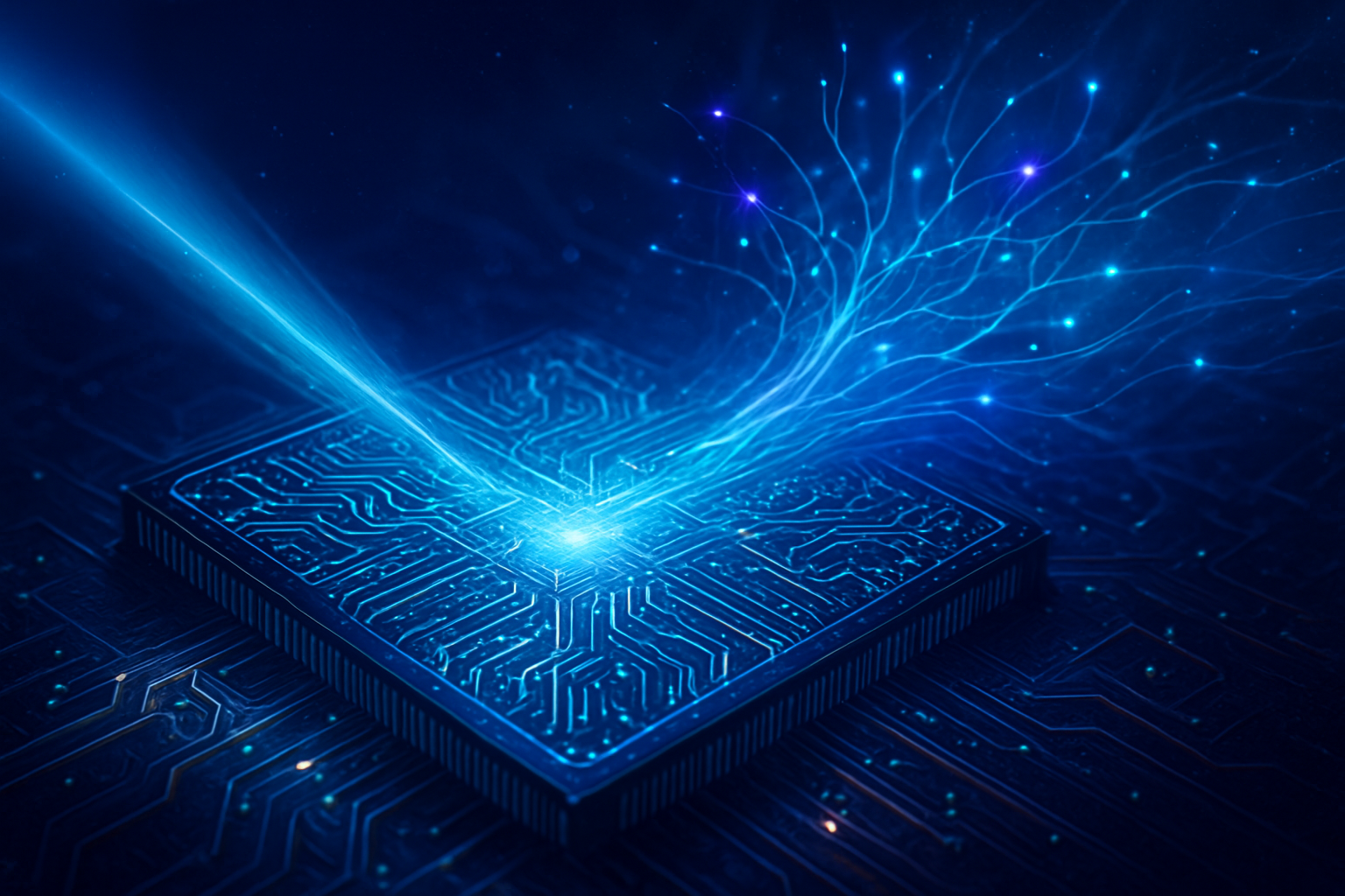
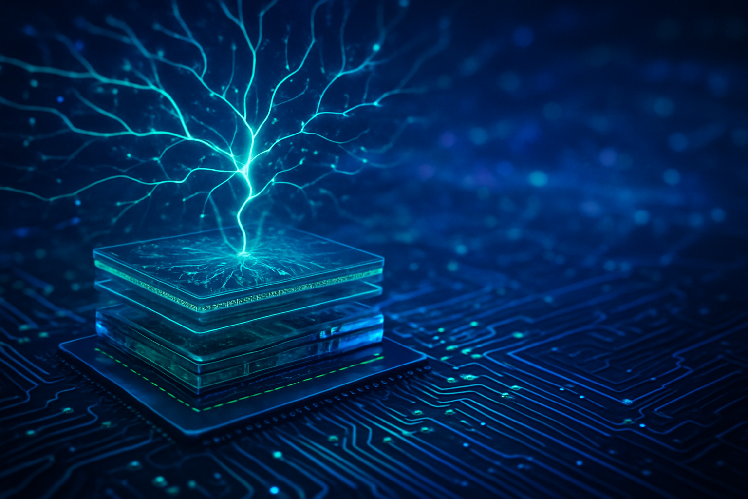
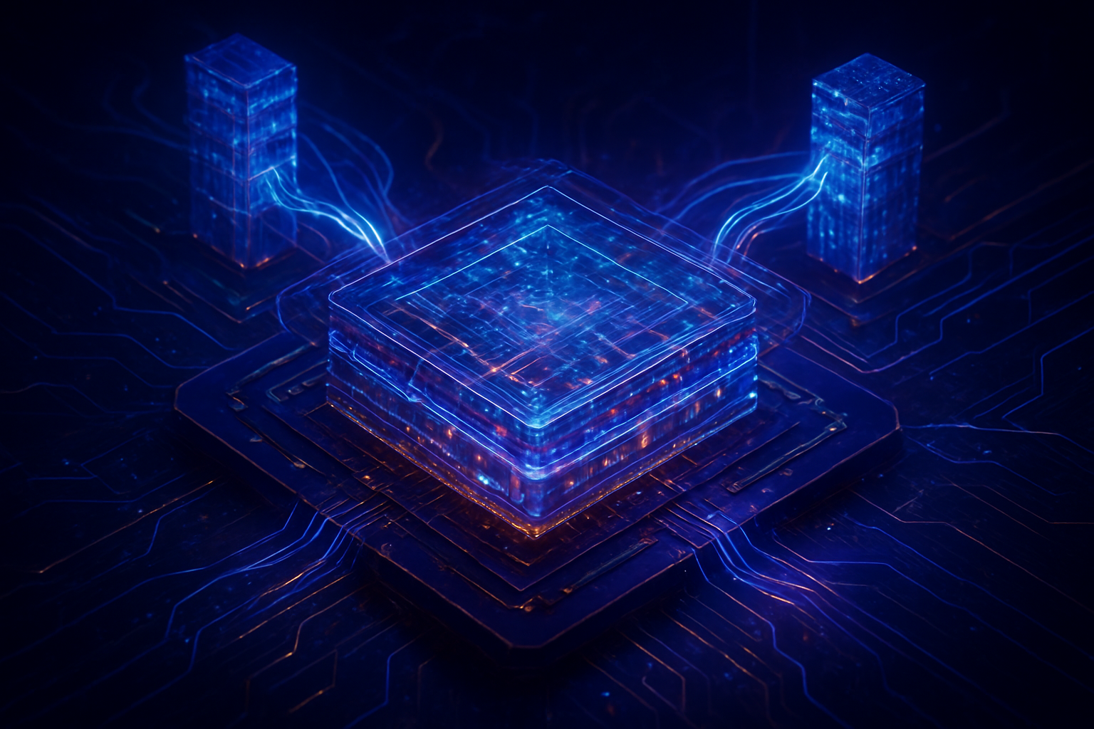
    Technically, advanced packaging primarily revolves around 2.5D and 3D integration. In 2.5D integration, multiple active dies, such as a GPU and several HBM stacks, are placed side-by-side on a high-density intermediate substrate called an interposer. This interposer, often silicon-based with fine Redistribution Layers (RDLs) and Through-Silicon Vias (TSVs), dramatically reduces die-to-die interconnect length, improving signal integrity, lowering latency, and reducing power consumption compared to traditional PCB traces. NVIDIA (NASDAQ: NVDA) H100 GPUs, utilizing TSMC's (NYSE: TSM) CoWoS (Chip-on-Wafer-on-Substrate) technology, are a prime example. In contrast, 3D integration involves vertically stacking multiple dies and connecting them via TSVs for ultrafast signal transfer. A key advancement here is hybrid bonding, which directly connects metal pads on devices without bumps, allowing for significantly higher interconnect density. Samsung's (KRX: 005930) HBM-PIM (Processing-in-Memory) and TSMC's SoIC (System-on-Integrated-Chips) are leading 3D stacking technologies, with mass production for SoIC planned for 2025. HBM itself is a critical component, achieving high bandwidth by vertically stacking multiple DRAM dies using TSVs and a wide I/O interface (e.g., 1024 bits for HBM vs. 32 bits for GDDR), providing massive bandwidth and power efficiency.

    This differs fundamentally from previous 2D packaging approaches, where a single die is attached to a substrate, leading to long interconnects on the PCB that introduce latency, increase power consumption, and limit bandwidth. 2.5D and 3D integration directly address these limitations by bringing dies much closer, dramatically reducing interconnect lengths and enabling significantly higher communication bandwidth and power efficiency. Initial reactions from the AI research community and industry experts have been overwhelmingly positive, viewing advanced packaging as a crucial and transformative development. They recognize it as pivotal for the future of AI, enabling the industry to overcome Moore's Law limits and sustain the "AI boom." Industry forecasts predict the market share of advanced packaging will double by 2030, with major players like TSMC, Intel (NASDAQ: INTC), Samsung, Micron (NASDAQ: MU), and SK Hynix (KRX: 000660) making substantial investments and aggressively expanding capacity. While the benefits are clear, challenges remain, including manufacturing complexity, high cost, and thermal management for dense 3D stacks, along with the need for standardization.

    Corporate Chessboard: Beneficiaries, Battles, and Strategic Shifts

    Advanced chip packaging is fundamentally reshaping the landscape of the Artificial Intelligence (AI) industry, enabling the creation of faster, smaller, and more energy-efficient AI chips crucial for the escalating demands of modern AI models. This technological shift is driving significant competitive implications, potential disruptions, and strategic advantages for various companies across the semiconductor ecosystem.

    Tech giants are at the forefront of investing heavily in advanced packaging capabilities to maintain their competitive edge and satisfy the surging demand for AI hardware. This investment is critical for developing sophisticated AI accelerators, GPUs, and CPUs that power their AI infrastructure and cloud services. For startups, advanced packaging, particularly through chiplet architectures, offers a potential pathway to innovate. Chiplets can democratize AI hardware development by reducing the need for startups to design complex monolithic chips from scratch, instead allowing them to integrate specialized, pre-designed chiplets into a single package, potentially lowering entry barriers and accelerating product development.

    Several companies are poised to benefit significantly. NVIDIA (NASDAQ: NVDA), a dominant force in AI GPUs, heavily relies on HBM integrated through TSMC's CoWoS technology for its high-performance accelerators like the H100 and Blackwell GPUs, and is actively shifting to newer CoWoS-L technology. TSMC (NYSE: TSM), as a leading pure-play foundry, is unparalleled in advanced packaging with its 3DFabric suite (CoWoS and SoIC), aggressively expanding CoWoS capacity to quadruple output by the end of 2025. Intel (NASDAQ: INTC) is heavily investing in its Foveros (true 3D stacking) and EMIB (Embedded Multi-die Interconnect Bridge) technologies, expanding facilities in the US to gain a strategic advantage. Samsung (KRX: 005930) is also a key player, investing significantly in advanced packaging, including a $7 billion factory and its SAINT brand for 3D chip packaging, making it a strategic partner for companies like OpenAI. AMD (NASDAQ: AMD) has pioneered chiplet-based designs for its CPUs and Instinct AI accelerators, leveraging 3D stacking and HBM. Memory giants Micron (NASDAQ: MU) and SK Hynix (KRX: 000660) hold dominant positions in the HBM market, making substantial investments in advanced packaging plants and R&D to supply critical HBM for AI GPUs.

    The rise of advanced packaging is creating new competitive battlegrounds. Competitive advantage is increasingly shifting towards companies with strong foundry access and deep expertise in packaging technologies. Foundry giants like TSMC, Intel, and Samsung are leading this charge with massive investments, making it challenging for others to catch up. TSMC, in particular, has an unparalleled position in advanced packaging for AI chips. The market is seeing consolidation and collaboration, with foundries becoming vertically integrated solution providers. Companies mastering these technologies can offer superior performance-per-watt and more cost-effective solutions, putting pressure on competitors. This fundamental shift also means value is migrating from traditional chip design to integrated, system-level solutions, forcing companies to adapt their business models. Advanced packaging provides strategic advantages through performance differentiation, enabling heterogeneous integration, offering cost-effectiveness and flexibility through chiplet architectures, and strengthening supply chain resilience through domestic investments.

    Broader Horizons: AI's New Physical Frontier

    Advanced chip packaging is emerging as a critical enabler for the continued advancement and broader deployment of Artificial Intelligence (AI), fundamentally reshaping the semiconductor landscape. It addresses the growing limitations of traditional transistor scaling (Moore's Law) by integrating multiple components into a single package, offering significant improvements in performance, power efficiency, cost, and form factor for AI systems.

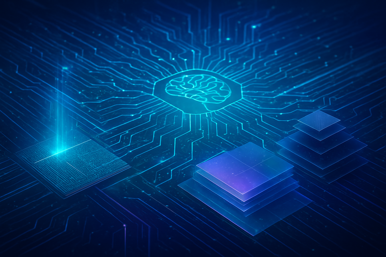
    This technology is indispensable for current and future AI trends. It directly overcomes Moore's Law limits by providing a new pathway to performance scaling through heterogeneous integration of diverse components. For power-hungry AI models, especially large generative language models, advanced packaging enables the creation of compact and powerful AI accelerators by co-packaging logic and memory with optimized interconnects, directly addressing the "memory wall" and "power wall" challenges. It supports AI across the computing spectrum, from edge devices to hyperscale data centers, and offers customization and flexibility through modular chiplet architectures. Intriguingly, AI itself is being leveraged to design and optimize chiplets and packaging layouts, enhancing power and thermal performance through machine learning.

    The impact of advanced packaging on AI is transformative, leading to significant performance gains by reducing signal delay and enhancing data transmission speeds through shorter interconnect distances. It also dramatically improves power efficiency, leading to more sustainable data centers and extended battery life for AI-powered edge devices. Miniaturization and a smaller form factor are also key benefits, enabling smaller, more portable AI-powered devices. Furthermore, chiplet architectures improve cost efficiency by reducing manufacturing costs and improving yield rates for high-end chips, while also offering scalability and flexibility to meet increasing AI demands.

    Despite its significant advantages, advanced packaging presents several concerns. The increased manufacturing complexity translates to higher costs, with packaging costs for top-end AI chips projected to climb significantly. The high density and complex connectivity introduce significant hurdles in design, assembly, and manufacturing validation, impacting yield and long-term reliability. Supply chain resilience is also a concern, as the market is heavily concentrated in the Asia-Pacific region, raising geopolitical anxieties. Thermal management is a major challenge due to densely packed, vertically integrated chips generating substantial heat, requiring innovative cooling solutions. Finally, the lack of universal standards for chiplet interfaces and packaging technologies can hinder widespread adoption and interoperability.

    Advanced packaging represents a fundamental shift in hardware development for AI, comparable in significance to earlier breakthroughs. Unlike previous AI milestones that often focused on algorithmic innovations, this is a foundational hardware milestone that makes software-driven advancements practically feasible and scalable. It signifies a strategic shift from traditional transistor scaling to architectural innovation at the packaging level, akin to the introduction of multi-core processors. Just as GPUs catalyzed the deep learning revolution, advanced packaging is providing the next hardware foundation, pushing beyond the limits of traditional GPUs to achieve more specialized and efficient AI processing, enabling an "AI-everywhere" world.

    The Road Ahead: Innovations and Challenges on the Horizon

    Advanced chip packaging is rapidly becoming a cornerstone of artificial intelligence (AI) development, surpassing traditional transistor scaling as a key enabler for high-performance, energy-efficient, and compact AI chips. This shift is driven by the escalating computational demands of AI, particularly large language models (LLMs) and generative AI, which require unprecedented memory bandwidth, low latency, and power efficiency. The market for advanced packaging in AI chips is experiencing explosive growth, projected to reach approximately $75 billion by 2033.

    In the near term (next 1-5 years), advanced packaging for AI will see the refinement and broader adoption of existing and maturing technologies. 2.5D and 3D integration, along with High Bandwidth Memory (HBM3 and HBM3e standards), will continue to be pivotal, pushing memory speeds and overcoming the "memory wall." Modular chiplet architectures are gaining traction, leveraging efficient interconnects like the UCIe standard for enhanced design flexibility and cost reduction. Fan-Out Wafer-Level Packaging (FOWLP) and its evolution, FOPLP, are seeing significant advancements for higher density and improved thermal performance, expected to converge with 2.5D and 3D integration to form hybrid solutions. Hybrid bonding will see further refinement, enabling even finer interconnect pitches. Co-Packaged Optics (CPO) are also expected to become more prevalent, offering significantly higher bandwidth and lower power consumption for inter-chiplet communication, with companies like Intel partnering on CPO solutions. Crucially, AI itself is being leveraged to optimize chiplet and packaging layouts, enhance power and thermal performance, and streamline chip design.

    Looking further ahead (beyond 5 years), the long-term trajectory involves even more transformative technologies. Modular chiplet architectures will become standard, tailored specifically for diverse AI workloads. Active interposers, embedded with transistors, will enhance in-package functionality, moving beyond passive silicon interposers. Innovations like glass-core substrates and 3.5D architectures will mature, offering improved performance and power delivery. Next-generation lithography technologies could re-emerge, pushing resolutions beyond current capabilities and enabling fundamental changes in chip structures, such as in-memory computing. 3D memory integration will continue to evolve, with an emphasis on greater capacity, bandwidth, and power efficiency, potentially moving towards more complex 3D integration with embedded Deep Trench Capacitors (DTCs) for power delivery.

    These advanced packaging solutions are critical enablers for the expansion of AI across various sectors. They are essential for the next leap in LLM performance, AI training efficiency, and inference speed in HPC and data centers, enabling compact, powerful AI accelerators. Edge AI and autonomous systems will benefit from enhanced smart devices with real-time analytics and minimal power consumption. Telecommunications (5G/6G) will see support for antenna-in-package designs and edge computing, while automotive and healthcare will leverage integrated sensor and processing units for real-time decision-making and biocompatible devices. Generative AI (GenAI) and LLMs will be significant drivers, requiring complicated designs including HBM, 2.5D/3D packaging, and heterogeneous integration.

    Despite the promising future, several challenges must be overcome. Manufacturing complexity and cost remain high, especially for precision alignment and achieving high yields and reliability. Thermal management is a major issue as power density increases, necessitating new cooling solutions like liquid and vapor chamber technologies. The lack of universal standards for chiplet interfaces and packaging technologies can hinder widespread adoption and interoperability. Supply chain constraints, design and simulation challenges requiring sophisticated EDA software, and the need for new material innovations to address thermal expansion and heat transfer are also critical hurdles. Experts are highly optimistic, predicting that the market share of advanced packaging will double by 2030, with continuous refinement of hybrid bonding and the maturation of the UCIe ecosystem. Leading players like TSMC, Samsung, and Intel are heavily investing in R&D and capacity, with the focus increasingly shifting from front-end (wafer fabrication) to back-end (packaging and testing) in the semiconductor value chain. AI chip package sizes are expected to triple by 2030, with hybrid bonding becoming preferred for cloud AI and autonomous driving after 2028, solidifying advanced packaging's role as a "foundational AI enabler."

    The Packaging Revolution: A New Era for AI

    In summary, innovations in chip packaging, or advanced packaging, are not just an incremental step but a fundamental revolution in how AI hardware is designed and manufactured. By enabling 2.5D and 3D integration, facilitating chiplet architectures, and leveraging High Bandwidth Memory (HBM), these technologies directly address the limitations of traditional silicon scaling, paving the way for unprecedented gains in AI performance, power efficiency, and form factor. This shift is critical for the continued development of complex AI models, from large language models to edge AI applications, effectively smashing the "memory wall" and providing the necessary computational infrastructure for the AI era.

    The significance of this development in AI history is profound, marking a transition from solely relying on transistor shrinkage to embracing architectural innovation at the packaging level. It's a hardware milestone as impactful as the advent of GPUs for deep learning, enabling the practical realization and scaling of cutting-edge AI software. Companies like NVIDIA (NASDAQ: NVDA), TSMC (NYSE: TSM), Intel (NASDAQ: INTC), Samsung (KRX: 005930), AMD (NASDAQ: AMD), Micron (NASDAQ: MU), and SK Hynix (KRX: 000660) are at the forefront of this transformation, investing billions to secure their market positions and drive future advancements. Their strategic moves in expanding capacity and refining technologies like CoWoS, Foveros, and HBM are shaping the competitive landscape of the AI industry.

    Looking ahead, the long-term impact will see increasingly modular, heterogeneous, and power-efficient AI systems. We can expect further advancements in hybrid bonding, co-packaged optics, and even AI-driven chip design itself. While challenges such as manufacturing complexity, high costs, thermal management, and the need for standardization persist, the relentless demand for more powerful AI ensures continued innovation in this space. The market for advanced packaging in AI chips is projected to grow exponentially, cementing its role as a foundational AI enabler.

    What to watch for in the coming weeks and months includes further announcements from leading foundries and memory manufacturers regarding capacity expansions and new technology roadmaps. Pay close attention to progress in chiplet standardization efforts, which will be crucial for broader adoption and interoperability. Also, keep an eye on how new cooling solutions and materials address the thermal challenges of increasingly dense packages. The packaging revolution is well underway, and its trajectory will largely dictate the pace and potential of AI innovation for years to come.


    This content is intended for informational purposes only and represents analysis of current AI developments.

    TokenRing AI delivers enterprise-grade solutions for multi-agent AI workflow orchestration, AI-powered development tools, and seamless remote collaboration platforms.
    For more information, visit https://www.tokenring.ai/.

  • Emerging Lithography: The Atomic Forge of Next-Gen AI Chips

    Emerging Lithography: The Atomic Forge of Next-Gen AI Chips

    The relentless pursuit of more powerful, efficient, and specialized Artificial Intelligence (AI) chips is driving a profound transformation in semiconductor manufacturing. At the heart of this revolution are emerging lithography technologies, particularly advanced Extreme Ultraviolet (EUV) and the re-emerging X-ray lithography, poised to unlock unprecedented levels of miniaturization and computational prowess. These advancements are not merely incremental improvements; they represent a fundamental shift in how the foundational hardware for AI is conceived and produced, directly fueling the explosive growth of generative AI and other data-intensive applications. The immediate significance lies in their ability to overcome the physical and economic limitations of current chip-making methods, paving the way for denser, faster, and more energy-efficient AI processors that will redefine the capabilities of AI systems from hyperscale data centers to the most compact edge devices.

    The Microscopic Art: X-ray Lithography's Resurgence and the EUV Frontier

    The quest for ever-smaller transistors has pushed optical lithography to its limits, making advanced techniques indispensable. X-ray lithography (XRL), a technology with a storied but challenging past, is making a compelling comeback, offering a potential pathway beyond the capabilities of even the most advanced Extreme Ultraviolet (EUV) systems.

    X-ray lithography operates on the principle of using X-rays, typically with wavelengths below 1 nanometer (nm), to transfer intricate patterns onto silicon wafers. This ultra-short wavelength provides an intrinsic resolution advantage, minimizing diffraction effects that plague longer-wavelength light sources. Modern XRL systems, such as those being developed by the U.S. startup Substrate, leverage particle accelerators to generate exceptionally bright X-ray beams, capable of achieving resolutions equivalent to the 2 nm semiconductor node and beyond. These systems can print features like random vias with a 30 nm center-to-center pitch and random logic contact arrays with 12 nm critical dimensions, showcasing a level of precision previously deemed unattainable. Unlike EUV, XRL typically avoids complex refractive lenses, and its X-rays exhibit negligible scattering within the resist, preventing issues like standing waves and reflection-based problems, which often limit resolution in other optical methods. Masks for XRL consist of X-ray absorbing materials like gold on X-ray transparent membranes, often silicon carbide or diamond.

    This technical prowess directly challenges the current state-of-the-art, EUV lithography, which utilizes 13.5 nm wavelength light to produce features down to 13 nm (Low-NA) and 8 nm (High-NA). While EUV has been instrumental in enabling current-generation advanced chips, XRL’s shorter wavelengths inherently offer greater resolution potential, with claims of surpassing the 2 nm node. Crucially, XRL has the potential to eliminate the need for multi-patterning, a complex and costly technique often required in EUV to achieve features beyond its optical limits. Furthermore, EUV systems require an ultra-high vacuum environment and highly reflective mirrors, which introduce challenges related to contamination and outgassing. Companies like Substrate claim that XRL could drastically reduce the cost of producing leading-edge wafers from an estimated $100,000 to approximately $10,000 by the end of the decade, by simplifying the optical system and potentially enabling a vertically integrated foundry model.

    The AI research community and industry experts view these developments with a mix of cautious optimism and skepticism. There is widespread recognition of the "immense potential for breakthroughs in chip performance and cost" that XRL could bring, especially given the escalating costs of current advanced chip fabrication. The technology is seen as a potential extension of Moore’s Law and a means to democratize access to advanced nodes. However, skepticism is tempered by the historical challenges XRL has faced, having been largely abandoned around 2000 due to issues like proximity lithography requirements, mask size limitations, and uniformity. Experts are keenly awaiting independent verification of these new XRL systems at scale, details on manufacturing partnerships, and concrete timelines for mass production, cautioning that mastering such precision typically takes a decade.

    Reshaping the Chipmaking Colossus: Corporate Beneficiaries and Competitive Shifts

    The advancements in lithography are not just technical marvels; they are strategic battlegrounds that will determine the future leadership in the semiconductor and AI industries. Companies positioned at the forefront of lithography equipment and advanced chip manufacturing stand to gain immense competitive advantages.

    ASML Holding N.V. (AMS: ASML), as the sole global supplier of EUV lithography machines, remains the undisputed linchpin of advanced chip manufacturing. Its continuous innovation, particularly in developing High-NA EUV systems, directly underpins the progress of the entire semiconductor industry, making it an indispensable partner for any company aiming for cutting-edge AI hardware. Foundries like Taiwan Semiconductor Manufacturing Company Limited (NYSE: TSM) and Samsung Electronics Co., Ltd. (KRX: 005930) are ASML's largest customers, making substantial investments in both current and next-generation EUV technologies. Their ability to produce the most advanced AI chips is directly tied to their access to and expertise with these lithography systems. Intel Corporation (NASDAQ: INTC), with its renewed foundry ambitions, is an early adopter of High-NA EUV, having already deployed two ASML High-NA EUV systems for R&D. This proactive approach could give Intel a strategic advantage in developing its upcoming process technologies and competing with leading foundries.

    Fabless semiconductor giants like NVIDIA Corporation (NASDAQ: NVDA) and Advanced Micro Devices, Inc. (NASDAQ: AMD), which design high-performance GPUs and CPUs crucial for AI workloads, rely entirely on their foundry partners' ability to leverage advanced lithography. More powerful and energy-efficient chips enabled by smaller nodes translate directly to faster training of large language models and more efficient AI inference for these companies. Moreover, emerging AI startups stand to benefit significantly. Advanced lithography enables the creation of specialized, high-performance, and energy-efficient AI chips, accelerating AI research and development and potentially lowering operational costs for AI accelerators. The prospect of reduced manufacturing costs through innovations like next-generation X-ray lithography could also lower the barrier to entry for smaller players, fostering a more diversified AI hardware ecosystem.

    However, the emergence of X-ray lithography from companies like Substrate presents a potentially significant disruption. If successful in drastically reducing the capital expenditure for advanced semiconductor manufacturing (from an estimated $100,000 to $10,000 per wafer), XRL could fundamentally alter the competitive landscape. It could challenge ASML's dominance in lithography equipment and TSMC's and Samsung's leadership in advanced node manufacturing, potentially democratizing access to cutting-edge chip production. While EUV is the current standard, XRL's ability to achieve finer features and higher transistor densities, coupled with potentially lower costs, offers profound strategic advantages to those who successfully adopt it. Yet, the historical challenges of XRL and the complexity of building an entire ecosystem around a new technology remain formidable hurdles that temper expectations.

    A New Era for AI: Broader Significance and Societal Ripples

    The advancements in lithography and the resulting AI hardware are not just technical feats; they are foundational shifts that will reshape the broader AI landscape, carrying significant societal implications and marking a pivotal moment in AI's developmental trajectory.

    These emerging lithography technologies are directly fueling several critical AI trends. They enable the development of more powerful and complex AI models, pushing the boundaries of generative AI, scientific discovery, and complex simulations by providing the necessary computational density and memory bandwidth. The ability to produce smaller, more power-efficient chips is also crucial for the proliferation of ubiquitous edge AI, extending AI capabilities from centralized data centers to devices like smartphones, autonomous vehicles, and IoT sensors. This facilitates real-time decision-making, reduced latency, and enhanced privacy by processing data locally. Furthermore, the industry is embracing a holistic hardware development approach, combining ultra-precise patterning from lithography with novel materials and sophisticated 3D stacking/chiplet architectures to overcome the physical limits of traditional transistor scaling. Intriguingly, AI itself is playing an increasingly vital role in chip creation, with AI-powered Electronic Design Automation (EDA) tools automating complex design tasks and optimizing manufacturing processes, creating a self-improving loop where AI aids in its own advancement.

    The societal implications are far-reaching. While the semiconductor industry is projected to reach $1 trillion by 2030, largely driven by AI, there are concerns about potential job displacement due to AI automation and increased economic inequality. The concentration of advanced lithography in a few regions and companies, such as ASML's (AMS: ASML) monopoly on EUV, creates supply chain vulnerabilities and could exacerbate a digital divide, concentrating AI power among a few well-resourced players. More powerful AI also raises significant ethical questions regarding bias, algorithmic transparency, privacy, and accountability. The environmental impact is another growing concern, with advanced chip manufacturing being highly resource-intensive and AI-optimized data centers consuming significant electricity, contributing to a quadrupling of global AI chip manufacturing emissions in recent years.

    In the context of AI history, these lithography advancements are comparable to foundational breakthroughs like the invention of the transistor or the advent of Graphics Processing Units (GPUs) with technologies like NVIDIA's (NASDAQ: NVDA) CUDA, which catalyzed the deep learning revolution. Just as transistors replaced vacuum tubes and GPUs provided the parallel processing power for neural networks, today's advanced lithography extends this scaling to near-atomic levels, providing the "next hardware foundation." Unlike previous AI milestones that often focused on algorithmic innovations, the current era highlights a profound interplay where hardware capabilities, driven by lithography, are indispensable for realizing algorithmic advancements. The demands of AI are now directly shaping the future of chip manufacturing, driving an urgent re-evaluation and advancement of production technologies.

    The Road Ahead: Navigating the Future of AI Chip Manufacturing

    The evolution of lithography for AI chips is a dynamic landscape, characterized by both near-term refinements and long-term disruptive potentials. The coming years will see a sustained push for greater precision, efficiency, and novel architectures.

    In the near term, the widespread adoption and refinement of High-Numerical Aperture (High-NA) EUV lithography will be paramount. High-NA EUV, with its 0.55 NA compared to current EUV's 0.33 NA, offers an 8 nm resolution, enabling transistors that are 1.7 times smaller and nearly triple the transistor density. This is considered the only viable path for high-volume production at 1.8 nm and below. Major players like Intel (NASDAQ: INTC) have already deployed High-NA EUV machines for R&D, with plans for product proof points on its Intel 18A node in 2025. TSMC (NYSE: TSM) expects to integrate High-NA EUV into its A14 (1.4 nm) process node for mass production around 2027. Alongside this, continuous optimization of current EUV systems, focusing on throughput, yield, and process stability, will remain crucial. Importantly, Artificial Intelligence and machine learning are rapidly being integrated into lithography process control, with AI algorithms analyzing vast datasets to predict defects and make proactive adjustments, potentially increasing yields by 15-20% at 5 nm nodes and below.

    Looking further ahead, the long-term developments will encompass even more disruptive technologies. The re-emergence of X-ray lithography, with companies like Substrate pushing for cost-effective production methods and resolutions beyond EUV, could be a game-changer. Directed Self-Assembly (DSA), a nanofabrication technique using block copolymers to create precise nanoscale patterns, offers potential for pattern rectification and extending the capabilities of existing lithography. Nanoimprint Lithography (NIL), led by companies like Canon, is gaining traction for its cost-effectiveness and high-resolution capabilities, potentially reproducing features below 5 nm with greater resolution and lower line-edge roughness. Furthermore, AI-powered Inverse Lithography Technology (ILT), which designs photomasks from desired wafer patterns using global optimization, is accelerating, pushing towards comprehensive full-chip optimization. These advancements are crucial for the continued growth of AI, enabling more powerful AI accelerators, ubiquitous edge AI devices, high-bandwidth memory (HBM), and novel chip architectures.

    Despite this rapid progress, significant challenges persist. The exorbitant cost of modern semiconductor fabs and cutting-edge EUV machines (High-NA EUV systems costing around $384 million) presents a substantial barrier. Technical complexity, particularly in defect detection and control at nanometer scales, remains a formidable hurdle, with issues like stochastics leading to pattern errors. The supply chain vulnerability, stemming from ASML's (AMS: ASML) sole supplier status for EUV scanners, creates a bottleneck. Material science also plays a critical role, with the need for novel resist materials and a shift away from PFAS-based chemicals. Achieving high throughput and yield for next-generation technologies like X-ray lithography comparable to EUV is another significant challenge. Experts predict a continued synergistic evolution between semiconductor manufacturing and AI, with EUV and High-NA EUV dominating leading-edge logic. AI and machine learning will increasingly transform process control and defect detection. The future of chip manufacturing is seen not just as incremental scaling but as a profound redefinition combining ultra-precise patterning, novel materials, and modular, vertically integrated designs like 3D stacking and chiplets.

    The Dawn of a New Silicon Age: A Comprehensive Wrap-Up

    The journey into the sub-nanometer realm of AI chip manufacturing, propelled by emerging lithography technologies, marks a transformative period in technological history. The key takeaways from this evolving landscape center on a multi-pronged approach to scaling: the continuous refinement of Extreme Ultraviolet (EUV) lithography and its next-generation High-NA EUV, the re-emergence of promising alternatives like X-ray lithography and Nanoimprint Lithography (NIL), and the increasingly crucial role of AI-powered lithography in optimizing every stage of the chip fabrication process. Technologies like Digital Lithography Technology (DLT) for advanced substrates and Multi-beam Electron Beam Lithography (MEBL) for increased interconnect density further underscore the breadth of innovation.

    The significance of these developments in AI history cannot be overstated. Just as the invention of the transistor laid the groundwork for modern computing and the advent of GPUs fueled the deep learning revolution, today's advanced lithography provides the "indispensable engines" for current and future AI breakthroughs. Without the ability to continually shrink transistor sizes and increase density, the computational power required for the vast scale and complexity of modern AI models, particularly generative AI, would be unattainable. Lithography enables chips with increased processing capabilities and lower power consumption, critical factors for AI hardware across all applications.

    The long-term impact of these emerging lithography technologies is nothing short of transformative. They promise a continuous acceleration of technological progress, yielding more powerful, efficient, and specialized computing devices that will fuel innovation across all sectors. These advancements are instrumental in meeting the ever-increasing computational demands of future technologies such as the metaverse, advanced autonomous systems, and pervasive smart environments. AI itself is poised to simplify the extreme complexities of advanced chip design and manufacturing, potentially leading to fully autonomous "lights-out" fabrication plants. Furthermore, lithography advancements will enable fundamental changes in chip structures, such as in-memory computing and novel architectures, coupled with heterogeneous integration and advanced packaging like 3D stacking and chiplets, pushing semiconductor performance to unprecedented levels. The global semiconductor market, largely propelled by AI, is projected to reach an unprecedented $1 trillion by 2030, a testament to this foundational progress.

    In the coming weeks and months, several critical developments bear watching. The deployment and performance improvements of High-NA EUV systems from ASML (AMS: ASML) will be closely scrutinized, particularly as Intel (NASDAQ: INTC) progresses with its Intel 18A node and TSMC (NYSE: TSM) plans for its A14 process. Keep an eye on further announcements regarding ASML's strategic investments in AI, as exemplified by its investment in Mistral AI in September 2025, aimed at embedding advanced AI capabilities directly into its lithography equipment to reduce defects and enhance yield. The commercial scaling and adoption of alternative technologies like X-ray lithography and Nanoimprint Lithography (NIL) from companies like Canon will also be a key indicator of future trends. China's progress in developing its domestic advanced lithography machines, including Deep Ultraviolet (DUV) and ambitions for indigenous EUV tools, will have significant geopolitical and economic implications. Finally, advancements in advanced packaging technologies, sustainability initiatives in chip manufacturing, and the sustained industry demand driven by the "AI supercycle" will continue to shape the future of AI hardware.


    This content is intended for informational purposes only and represents analysis of current AI developments.

    TokenRing AI delivers enterprise-grade solutions for multi-agent AI workflow orchestration, AI-powered development tools, and seamless remote collaboration platforms.
    For more information, visit https://www.tokenring.ai/.

  • Nvidia Shatters Records with $5 Trillion Valuation: A Testament to AI’s Unprecedented Economic Power

    Nvidia Shatters Records with $5 Trillion Valuation: A Testament to AI’s Unprecedented Economic Power

    In a monumental achievement that reverberates across the global technology landscape, NVIDIA Corporation (NASDAQ: NVDA) has officially reached an astonishing market valuation of $5 trillion. This unprecedented milestone, achieved on October 29, 2025, not only solidifies Nvidia's position as the world's most valuable company, surpassing tech titans like Apple (NASDAQ: AAPL) and Microsoft (NASDAQ: MSFT), but also serves as a stark, undeniable indicator of artificial intelligence's rapidly escalating economic might. The company's meteoric rise, adding a staggering $1 trillion to its market capitalization in just the last three months, underscores a seismic shift in economic power, firmly placing AI at the forefront of a new industrial revolution.

    Nvidia's journey to this historic valuation has been nothing short of spectacular, characterized by an accelerated pace that has left previous market leaders in its wake. From crossing the $1 trillion mark in June 2023 to hitting $2 trillion in March 2024—a feat accomplished in a mere 180 trading days—the company's growth trajectory has been fueled by an insatiable global demand for the computing power essential to developing and deploying advanced AI models. This $5 trillion valuation is not merely a number; it represents the immense investor confidence in Nvidia's indispensable role as the backbone of global AI infrastructure, a role that sees its advanced Graphics Processing Units (GPUs) powering everything from generative AI to autonomous vehicles and sophisticated robotics.

    The Unseen Engines of AI: Nvidia's Technical Prowess and Market Dominance

    Nvidia's stratospheric valuation is intrinsically linked to its unparalleled technical leadership in the field of AI, driven by a relentless pace of innovation in both hardware and software. At the core of its dominance are its state-of-the-art Graphics Processing Units (GPUs), which have become the de facto standard for AI training and inference. The H100 GPU, based on the Hopper architecture and built on a 5nm process with 80 billion transistors, exemplifies this prowess. Featuring fourth-generation Tensor Cores and a dedicated Transformer Engine with FP8 precision, the H100 delivers up to nine times faster training and an astonishing 30 times inference speedup for large language models compared to its predecessors. Its GH100 processor, with 16,896 shading units and 528 Tensor Cores, coupled with up to 96GB of HBM3 memory and the NVLink Switch System, enables exascale workloads by connecting up to 256 H100 GPUs with 900 GB/s bidirectional bandwidth.

    Looking ahead, Nvidia's recently unveiled Blackwell architecture, announced at GTC 2024, promises to redefine the generative AI era. Blackwell-architecture GPUs pack an incredible 208 billion transistors using a custom TSMC 4NP process, integrating two reticle-limited dies into a single, unified GPU. This architecture introduces fifth-generation Tensor Cores and native support for sub-8-bit data types like MXFP6 and MXFP4, effectively doubling performance and memory size for next-generation models while maintaining high accuracy. The GB200 Grace Blackwell Superchip, a cornerstone of this new architecture, integrates two high-performance Blackwell Tensor Core GPUs with an NVIDIA Grace CPU via the NVLink-C2C interconnect, creating a rack-scale system (GB200 NVL72) capable of 30x faster real-time trillion-parameter large language model inference.

    Beyond raw hardware, Nvidia's formidable competitive moat is significantly fortified by its comprehensive software ecosystem. The Compute Unified Device Architecture (CUDA) is Nvidia's proprietary parallel computing platform, providing developers with direct access to the GPU's power through a robust API. Since its inception in 2007, CUDA has cultivated a massive developer community, now supporting multiple programming languages and offering extensive libraries, debuggers, and optimization tools, making it the fundamental platform for AI and machine learning. Complementing CUDA are specialized libraries like cuDNN (CUDA Deep Neural Network library), which provides highly optimized routines for deep learning frameworks like TensorFlow and PyTorch, and TensorRT, an inference optimizer that can deliver up to 36 times faster inference performance by leveraging precision calibration, layer fusion, and automatic kernel tuning.

    This full-stack integration—from silicon to software—is what truly differentiates Nvidia from rivals like Advanced Micro Devices (NASDAQ: AMD) and Intel Corporation (NASDAQ: INTC). While AMD offers its Instinct GPUs with CDNA architecture and Intel provides Gaudi AI accelerators and Xeon CPUs for AI, neither has managed to replicate the breadth, maturity, or developer lock-in of Nvidia's CUDA ecosystem. Experts widely refer to CUDA as a "formidable barrier to entry" and a "durable moat," creating significant switching costs for customers deeply integrated into Nvidia's platform. The AI research community and industry experts consistently validate Nvidia's performance, with H100 GPUs being the industry standard for training large language models for tech giants, and the Blackwell architecture being heralded by CEOs of Google (NASDAQ: GOOGL), Meta Platforms (NASDAQ: META), Microsoft (NASDAQ: MSFT), and OpenAI as the "processor for the generative AI era."

    Reshaping the AI Landscape: Corporate Impacts and Competitive Dynamics

    Nvidia's unprecedented market dominance, culminating in its $5 trillion valuation, is fundamentally reshaping the competitive dynamics across the entire AI industry, influencing tech giants, AI startups, and its vast supply chain. AI companies of all sizes find themselves deeply reliant on Nvidia's GPUs and the pervasive CUDA software ecosystem, which have become the foundational compute engines for training and deploying advanced AI models. This reliance means that the speed and scale of AI innovation for many are inextricably linked to the availability and cost of Nvidia's hardware, creating a significant ecosystem lock-in that makes switching to alternative solutions challenging and expensive.

    For major tech giants and hyperscale cloud providers such as Amazon (NASDAQ: AMZN), Google (NASDAQ: GOOGL), and Microsoft (NASDAQ: MSFT), Nvidia is an indispensable partner and a formidable force. These companies are among Nvidia's largest customers, procuring vast quantities of GPUs to power their expansive cloud AI services and internal research initiatives. While these hyperscalers are aggressively investing in developing their own custom AI silicon to mitigate dependency and gain greater control over their AI infrastructure, they continue to be substantial buyers of Nvidia's offerings due to their superior performance and established ecosystem. Nvidia's strong market position allows it to significantly influence pricing and terms, directly impacting the operational costs and competitive strategies of these cloud AI behemoths.

    Nvidia's influence extends deeply into the AI startup ecosystem, where it acts not just as a hardware supplier but also as a strategic investor. Through its venture arm, Nvidia provides crucial capital, management expertise, and, most critically, access to its scarce and highly sought-after GPUs to numerous AI startups. Companies like Cohere (generative AI), Perplexity AI (AI search engine), and Reka AI (video analysis models) have benefited from Nvidia's backing, gaining vital resources that accelerate their development and solidify their market position. This strategic investment approach allows Nvidia to integrate advanced AI technologies into its own offerings, diversify its product portfolio, and effectively steer the trajectory of AI development, further reinforcing the centrality of its ecosystem.

    The competitive implications for rival chipmakers are profound. While companies like AMD (NASDAQ: AMD), Intel (NASDAQ: INTC), and Qualcomm (NASDAQ: QCOM) are actively developing their own AI accelerators—such as AMD's Instinct MI325 Series and Intel's Gaudi 3—they face an uphill battle against Nvidia's "nearly impregnable lead" and the deeply entrenched CUDA ecosystem. Nvidia's first-mover advantage, continuous innovation with architectures like Blackwell and the upcoming Rubin, and its full-stack AI strategy create a formidable barrier to entry. This dominance is not without scrutiny; Nvidia's accelerating market power has attracted global regulatory attention, with antitrust concerns being raised, particularly regarding its control over the CUDA software ecosystem and the impact of U.S. export controls on advanced AI chips to China.

    The Broader AI Canvas: Societal Impacts and Future Trajectories

    Nvidia's monumental $5 trillion valuation, achieved on October 29, 2025, transcends mere financial metrics; it serves as a powerful testament to the profound and accelerating impact of the AI revolution on the broader global landscape. Nvidia's GPUs and the ubiquitous CUDA software ecosystem have become the indispensable bedrock for AI model training and inference, effectively establishing the company as the foundational infrastructure provider for the AI age. Commanding an estimated 75% to 90% market share in the AI chip segment, with a staggering 92% share in data center GPUs, Nvidia's technological superiority and ecosystem lock-in have solidified its position with hyperscalers, cloud providers, and research institutions worldwide.

    This dominance is not just a commercial success story; it is a catalyst for a new industrial revolution. Nvidia's market capitalization now exceeds the GDP of several major nations, including Germany, India, Japan, and the United Kingdom, and surpasses the combined valuation of tech giants like Google (NASDAQ: GOOGL) and Meta Platforms (NASDAQ: META). Its stock performance has become a primary driver for the recent surge in global financial markets, firmly establishing AI as the central investment theme of the decade. This AI boom, with Nvidia at its "epicenter," is widely considered the next major industrial revolution, comparable to those driven by steam, electricity, and information technology, as industries leverage AI to unlock vast amounts of previously unused data.

    The impacts ripple across diverse sectors, fundamentally transforming industries and society. In healthcare and drug discovery, Nvidia's GPUs are accelerating breakthroughs, leading to faster research and development. In the automotive sector, partnerships with companies like Uber (NYSE: UBER) for robotaxis signal a significant shift towards fully autonomous vehicles. Manufacturing and robotics are being revolutionized by agentic AI and digital twins, enabling more intelligent factories and seamless human-robot interaction, potentially leading to a sharp decrease in the cost of industrial robots. Even traditional sectors like retail are seeing intelligent stores, optimized merchandising, and efficient supply chains powered by Nvidia's technology, while collaborations with telecommunications giants like Nokia (NYSE: NOK) on 6G technology point to future advancements in networking and data centers.

    However, Nvidia's unprecedented growth and market concentration also raise significant concerns. The immense power concentrated in Nvidia's hands, alongside a few other major AI players, has sparked warnings of a potential "AI bubble" with overheated valuations. The circular nature of some investments, such as Nvidia's investment in OpenAI (one of its largest customers), further fuels these concerns, with some analysts drawing parallels to the 2008 financial crisis if AI promises fall short. Global regulators, including the Bank of England and the IMF, have also flagged these risks. Furthermore, the high cost of advanced AI hardware and the technical expertise required can pose significant barriers to entry for individuals and smaller businesses, though cloud-based AI platforms are emerging to democratize access. Nvidia's dominance has also placed it at the center of geopolitical tensions, particularly the US-China tech rivalry, with US export controls on advanced AI chips impacting a significant portion of Nvidia's revenue from China sales and raising concerns from CEO Jensen Huang about long-term American technological leadership.

    The Horizon of AI: Expected Developments and Emerging Challenges

    Nvidia's trajectory in the AI landscape is poised for continued and significant evolution in the coming years, driven by an aggressive roadmap of hardware and software innovations, an expanding application ecosystem, and strategic partnerships. In the near term, the Blackwell architecture, announced at GTC 2024, remains central. Blackwell-architecture GPUs like the B100 and B200, with their 208 billion transistors and second-generation Transformer Engine, are purpose-built for generative AI workloads, accelerating large language model (LLM) training and inference. These chips, featuring new precisions and confidential computing capabilities, are already reportedly sold out for 2025 production, indicating sustained demand. The consumer-focused GeForce RTX 50 series, also powered by Blackwell, saw its initial launches in early 2025.

    Looking further ahead, Nvidia has unveiled its successor to Blackwell: the Vera Rubin Superchip, slated for mass production around Q3/Q4 2026, with the "Rubin Ultra" variant following in 2027. The Rubin architecture, named after astrophysicist Vera Rubin, will consist of a Rubin GPU and a Vera CPU, manufactured by TSMC using a 3nm process and utilizing HBM4 memory. These GPUs are projected to achieve 50 petaflops in FP4 performance, with Rubin Ultra doubling that to 100 petaflops. Nvidia is also pioneering NVQLink, an open architecture designed to tightly couple GPU supercomputing with quantum processors, signaling a strategic move towards hybrid quantum-classical computing. This continuous, yearly release cadence for data center products underscores Nvidia's commitment to maintaining its technological edge.

    Nvidia's proprietary CUDA software ecosystem remains a formidable competitive moat, with over 3 million developers and 98% of AI developers using the platform. In the near term, Nvidia continues to optimize CUDA for LLMs and inference engines, with its NeMo Framework and TensorRT-LLM integral to the Blackwell architecture's Transformer Engine. The company is also heavily focused on agentic AI, with the NeMo Agent Toolkit being a key software component. Notably, in October 2025, Nvidia announced it would open-source its Aerial software, including Aerial CUDA-Accelerated RAN, Aerial Omniverse Digital Twin (AODT), and the new Aerial Framework, empowering developers to build AI-native 5G and 6G RAN solutions. Long-term, Nvidia's partnership with Nokia (NYSE: NOK) to create an AI-RAN (Radio Access Network) platform, unifying AI and radio access workloads on an accelerated infrastructure for 5G-Advanced and 6G networks, showcases its ambition to embed AI into critical telecommunications infrastructure.

    The potential applications and use cases on the horizon are vast and transformative. Beyond generative AI and LLMs, Nvidia is a pivotal player in autonomous systems, collaborating with companies like Uber (NYSE: UBER), GM (NYSE: GM), and Mercedes-Benz (ETR: MBG) to develop self-driving platforms and launch autonomous fleets, with Uber aiming for 100,000 robotaxis by 2027. In scientific computing and climate modeling, Nvidia is building seven new supercomputers for the U.S. Department of Energy, including the largest, Solstice, deploying 100,000 Blackwell GPUs for scientific discovery and climate simulations. Healthcare and life sciences will see accelerated drug discovery, medical imaging, and personalized medicine, while manufacturing and industrial AI will leverage Nvidia's Omniverse platform and agentic AI for intelligent factories and "auto-pilot" chip design systems.

    Despite this promising outlook, significant challenges loom. Power consumption remains a critical concern as AI models grow, prompting Nvidia's "extreme co-design" approach and the development of more efficient architectures like Rubin. Competition is intensifying, with hyperscalers like Google (NASDAQ: GOOGL), Amazon (NASDAQ: AMZN), and Microsoft (NASDAQ: MSFT) heavily investing in custom AI silicon (e.g., TPUs, Trainium, Maia 100) to reduce dependency. Rival chipmakers like AMD (NASDAQ: AMD), Intel (NASDAQ: INTC), and Qualcomm (NASDAQ: QCOM) are also making concerted efforts to capture market share in data center and edge AI. Ethical considerations, including bias, privacy, and control, are paramount, with Nvidia emphasizing "Trustworthy AI" and states passing new AI safety and privacy laws. Finally, geopolitical tensions and U.S. export controls on advanced AI chips continue to impact Nvidia's market access in China, significantly affecting its revenue from the region and raising concerns from CEO Jensen Huang about long-term American technological leadership. Experts, however, generally predict Nvidia will maintain its leadership in high-end AI training and accelerated computing through continuous innovation and the formidable strength of its CUDA ecosystem, with some analysts forecasting a potential $6 trillion market capitalization by late 2026.

    A New Epoch: Nvidia's Defining Role in AI History

    Nvidia's market valuation soaring past $5 trillion on October 29, 2025, is far more than a financial headline; it marks a new epoch in AI history, cementing the company's indispensable role as the architect of the artificial intelligence revolution. This extraordinary ascent, from $1 trillion in May 2023 to $5 trillion in a little over two years, underscores the unprecedented demand for AI computing power and Nvidia's near-monopoly in providing the foundational infrastructure for this transformative technology. The company's estimated 86% control of the AI GPU market as of October 29, 2025 is a testament to its unparalleled hardware superiority, the strategic brilliance of its CUDA software ecosystem, and its foresight in anticipating the "AI supercycle."

    The key takeaways from Nvidia's explosive growth are manifold. Firstly, Nvidia has unequivocally transitioned from a graphics card manufacturer to the essential infrastructure provider of the AI era, making its GPUs and software ecosystem fundamental to global AI development. Secondly, the CUDA platform acts as an unassailable "moat," creating significant switching costs and deeply embedding Nvidia's hardware into the workflows of developers and enterprises worldwide. Thirdly, Nvidia's impact extends far beyond data centers, driving innovation across diverse sectors including autonomous driving, robotics, healthcare, and smart manufacturing. Lastly, the company's rapid innovation cycle, capable of producing new chips every six months, ensures it remains at the forefront of technological advancement.

    Nvidia's significance in AI history is profound and transformative. Its seminal step in 2006 with the release of CUDA, which unlocked the parallel processing capabilities of GPUs for general-purpose computing, proved prescient. This innovation laid the groundwork for the deep learning revolution of the 2010s, with researchers demonstrating that Nvidia GPUs could dramatically accelerate neural network training, effectively sparking the modern AI era. The company's hardware became the backbone for developing groundbreaking AI applications like OpenAI's ChatGPT, which was built upon 10,000 Nvidia GPUs. CEO Jensen Huang's vision, anticipating the broader application of GPUs beyond graphics and strategically investing in AI, has been instrumental in driving this technological revolution, fundamentally re-emphasizing hardware as a strategic differentiator in the semiconductor industry.

    Looking long-term, Nvidia is poised for continued robust growth, with analysts projecting the AI chip market to reach $621 billion by 2032. Its strategic pivots into AI infrastructure and open ecosystems, alongside diversification beyond hardware sales into areas like AI agents for industrial problems, will solidify its indispensable role in global AI development. However, this dominance also comes with inherent risks. Intensifying competition from rivals like AMD (NASDAQ: AMD), Intel (NASDAQ: INTC), and Qualcomm (NASDAQ: QCOM), as well as in-house accelerators from hyperscale cloud providers, threatens to erode its market share, particularly in the AI inference market. Geopolitical tensions, especially U.S.-China trade relations and export controls on advanced AI chips, remain a significant source of uncertainty, impacting Nvidia's market access in China. Concerns about a potential "AI bubble" also persist, with some analysts questioning the sustainability of rapid tech stock appreciation and the tangible returns on massive AI investments.

    In the coming weeks and months, all eyes will be on Nvidia's upcoming earnings reports for critical insights into its financial performance and management's commentary on market demand and competitive dynamics. The rollout of the Blackwell Ultra GB300 NVL72 in the second half of 2025 and the planned release of the Rubin platform in the second half of 2026, followed by Rubin Ultra in 2027, will be pivotal in showcasing next-generation AI capabilities. Developments from competitors, particularly in the inference market, and shifts in the geopolitical climate regarding AI chip exports, especially anticipated talks between President Trump and Xi Jinping about Nvidia's Blackwell chip, could significantly impact the company's trajectory. Ultimately, the question of whether enterprises begin to see tangible revenue returns from their significant AI infrastructure investments will dictate sustained demand for AI hardware and shape the future of this new AI epoch.


    This content is intended for informational purposes only and represents analysis of current AI developments.

    TokenRing AI delivers enterprise-grade solutions for multi-agent AI workflow orchestration, AI-powered development tools, and seamless remote collaboration platforms.
    For more information, visit https://www.tokenring.ai/.

  • AI Gold Rush: Semiconductor Giants NXP and Amkor Surge as Investment Pours into AI’s Hardware Foundation

    AI Gold Rush: Semiconductor Giants NXP and Amkor Surge as Investment Pours into AI’s Hardware Foundation

    The global technology landscape is undergoing a profound transformation, driven by the relentless advance of Artificial Intelligence, and at its very core, the semiconductor industry is experiencing an unprecedented boom. Companies like NXP Semiconductors (NASDAQ: NXPI) and Amkor Technology (NASDAQ: AMKR) are at the forefront of this revolution, witnessing significant stock surges as investors increasingly recognize their critical role in powering the AI future. This investment frenzy is not merely speculative; it is a direct reflection of the exponential growth of the AI market, which demands ever more sophisticated and specialized hardware to realize its full potential.

    These investment patterns signal a foundational shift, validating AI's economic impact and highlighting the indispensable nature of advanced semiconductors. As the AI market, projected to exceed $150 billion in 2025, continues its meteoric rise, the demand for high-performance computing, advanced packaging, and specialized edge processing solutions is driving capital towards key enablers in the semiconductor supply chain. The strategic positioning of companies like NXP in edge AI and automotive, and Amkor in advanced packaging, has placed them in prime position to capitalize on this AI-driven hardware imperative.

    The Technical Backbone of AI's Ascent: NXP's Edge Intelligence and Amkor's Packaging Prowess

    The surging investments in NXP Semiconductors and Amkor Technology are rooted in their distinct yet complementary technical advancements, which are proving instrumental in the widespread deployment of AI. NXP is spearheading the charge in edge AI, bringing sophisticated intelligence closer to the data source, while Amkor is mastering the art of advanced packaging, a critical enabler for the complex, high-performance AI chips that power everything from data centers to autonomous vehicles.

    NXP's technical contributions are particularly evident in its development of Discrete Neural Processing Units (DNPUs) and integrated NPUs within its i.MX 9 series applications processors. The Ara-1 Edge AI Discrete NPU, for instance, offers up to 6 equivalent TOPS (eTOPS) of performance, designed for real-time AI computing in embedded systems, supporting popular frameworks like TensorFlow and PyTorch. Its successor, the Ara-2, significantly ups the ante with up to 40 eTOPS, specifically engineered for real-time Generative AI, Large Language Models (LLMs), and Vision Language Models (VLMs) at the edge. What sets NXP's DNPUs apart is their efficient dataflow architecture, allowing for zero-latency context switching between multiple AI models—a significant leap from previous approaches that often incurred performance penalties when juggling different AI tasks. Furthermore, their i.MX 952 applications processor, with its integrated eIQ Neutron NPU, is tailored for AI-powered vision and human-machine interfaces in automotive and industrial sectors, combining low-power, real-time, and high-performance processing while meeting stringent functional safety standards like ISO 26262 ASIL B. The strategic acquisition of edge AI pioneer Kinara in February 2025 further solidified NXP's position, integrating high-performance, energy-efficient discrete NPUs into its portfolio.

    Amkor Technology, on the other hand, is the unsung hero of the AI hardware revolution, specializing in advanced packaging solutions that are indispensable for unlocking the full potential of modern AI chips. As traditional silicon scaling (Moore's Law) faces physical limits, heterogeneous integration—combining multiple dies into a single package—has become paramount. Amkor's expertise in 2.5D Through Silicon Via (TSV) interposers, Chip on Substrate (CoS), and Chip on Wafer (CoW) technologies allows for the high-bandwidth, low-latency interconnection of high-performance logic with high-bandwidth memory (HBM), which is crucial for AI and High-Performance Computing (HPC). Their innovative S-SWIFT (Silicon Wafer Integrated Fan-Out) technology offers a cost-effective alternative to 2.5D TSV, boosting I/O and circuit density while reducing package size and improving electrical performance, making it ideal for AI applications demanding significant memory and compute power. Amkor's impressive track record, including shipping over two million 2.5D TSV products and over 2 billion eWLB (embedded Wafer Level Ball Grid Array) components, underscores its maturity and capability in powering AI and HPC applications.

    Initial reactions from the AI research community and industry experts have been overwhelmingly positive for both companies. NXP's edge AI solutions are lauded for being "cost-effective, low-power solutions for vision processing and sensor fusion," empowering efficient and private machine learning at the edge. The Kinara acquisition is seen as a move that will "enhance and strengthen NXP's ability to provide complete and scalable AI platforms, from TinyML to generative AI." For Amkor, its advanced packaging capabilities are considered critical for the future of AI. NVIDIA (NASDAQ: NVDA) CEO Jensen Huang highlighted Amkor's $7 billion Arizona campus expansion as a "defining milestone" for U.S. leadership in the "AI century." Experts recognize Fan-Out Wafer Level Packaging (FOWLP) as a key enabler for heterogeneous integration, offering superior electrical performance and thermal dissipation, central to achieving performance gains beyond traditional transistor scaling. While NXP's Q3 2025 earnings saw some mixed market reaction due to revenue decline, analysts remain bullish on its long-term prospects in automotive and industrial AI. Investors are also closely monitoring Amkor's execution and ability to manage competition amidst its significant expansion.

    Reshaping the AI Ecosystem: From Hyperscalers to the Edge

    The robust investment in AI-driven semiconductor companies like NXP and Amkor is not merely a financial phenomenon; it is fundamentally reshaping the competitive landscape for AI companies, tech giants, and startups alike. As the global AI chip market barrels towards a projected $150 billion in 2025, access to advanced, specialized hardware is becoming the ultimate differentiator, driving both unprecedented opportunities and intense competitive pressures.

    Major tech giants, including Google (NASDAQ: GOOGL), Amazon (NASDAQ: AMZN), Microsoft (NASDAQ: MSFT), and Apple (NASDAQ: AAPL), are deeply entrenched in this race, often pursuing vertical integration by designing their own custom AI accelerators—such as Google's TPUs or Microsoft's Maia and Cobalt chips. This strategy aims to optimize performance for their unique AI workloads, reduce reliance on external suppliers like NVIDIA (NASDAQ: NVDA), and gain greater strategic control over their AI infrastructure. Their vast financial resources allow them to secure long-term contracts with leading foundries like TSMC (NYSE: TSM) and benefit from the explosive growth experienced by equipment suppliers like ASML (NASDAQ: ASML). This trend creates a dual dynamic: while it fuels demand for advanced manufacturing and packaging services from companies like Amkor, it also intensifies the competition for chip design talent and foundry capacity.

    For AI companies and startups, the proliferation of advanced AI semiconductors presents both a boon and a challenge. On one hand, the availability of more powerful, energy-efficient, and specialized chips—from NXP's edge NPUs to NVIDIA's data center GPUs—accelerates innovation and deployment across various sectors, enabling the training of larger models and the execution of more complex inference tasks. This democratizes access to AI capabilities to some extent, particularly with the rise of cloud-based design tools. However, the high costs associated with these cutting-edge chips and the intense demand from hyperscalers can create significant barriers for smaller players, potentially exacerbating an "AI divide" where only well-funded entities can fully leverage the latest hardware. Companies like NXP, with their focus on accessible edge AI solutions and comprehensive software stacks, offer a pathway for startups to embed sophisticated AI into their products without requiring massive data center investments.

    The market positioning and strategic advantages are increasingly defined by specialized expertise and ecosystem control. Companies like Amkor, with its leadership in advanced packaging technologies like 2.5D TSV and S-SWIFT, wield significant pricing power and importance as they solve the critical integration challenges for heterogeneous AI chips. NXP's strategic advantage lies in its deep penetration of the automotive and industrial IoT sectors, where its secure edge processing solutions and AI-optimized microcontrollers are becoming indispensable for real-time, low-power AI applications. The acquisition of Kinara, an edge AI chipmaker, further solidifies NXP's ability to provide complete and scalable AI platforms from TinyML to generative AI at the edge. This era also highlights the critical importance of robust software ecosystems, exemplified by NVIDIA's CUDA, which creates a powerful lock-in effect, tying developers and their applications to specific hardware platforms. The overall impact is a rapid evolution of products and services, with AI-enabled PCs projected to account for 43% of all PC shipments by the end of 2025, and new computing paradigms like neuromorphic and in-memory computing gaining traction, signaling a profound disruption to traditional computing architectures and an urgent imperative for continuous innovation.

    The Broader Canvas: AI Chips as the Bedrock of a New Era

    The escalating investment in AI-driven semiconductor companies transcends mere financial trends; it represents a foundational shift in the broader AI landscape, signaling a new era where hardware innovation is as critical as algorithmic breakthroughs. This intense focus on specialized chips, advanced packaging, and edge processing capabilities is not just enabling more powerful AI, but also reshaping global economies, igniting geopolitical competition, and presenting both immense opportunities and significant concerns.

    This current AI boom is distinguished by its sheer scale and speed of adoption, marking a departure from previous AI milestones that often centered more on software advancements. Today, AI's progress is deeply and symbiotically intertwined with hardware innovation, making the semiconductor industry the bedrock of this revolution. The demand for increasingly powerful, energy-efficient, and specialized chips—from NXP's DNPUs enabling generative AI at the edge to NVIDIA's cutting-edge Blackwell and Rubin architectures powering data centers—is driving relentless innovation in chip architecture, including the exploration of neuromorphic computing, quantum computing, and advanced 3D chip stacking. This technological leap is crucial for realizing the full potential of AI, enabling applications that were once confined to science fiction across healthcare, autonomous systems, finance, and manufacturing.

    However, this rapid expansion is not without its challenges and concerns. Economically, there are growing fears of an "AI bubble," with some analysts questioning whether the massive capital expenditure on AI infrastructure, such as Microsoft's planned $80 billion investment in AI data centers, is outpacing actual economic benefits. Reports of generative AI pilot programs failing to yield significant revenue returns in businesses add to this apprehension. The market also exhibits a high concentration of value among a few top players like NVIDIA (NASDAQ: NVDA) and TSMC (NYSE: TSM), raising questions about long-term market sustainability and potential vulnerabilities if the AI momentum falters. Environmentally, the resource-intensive nature of semiconductor manufacturing and the vast energy consumption of AI data centers pose significant challenges, necessitating a concerted effort towards energy-efficient designs and sustainable practices.

    Geopolitically, AI chips have become a central battleground, particularly between the United States and China. Considered dual-use technology with both commercial and strategic military applications, AI chips are now a focal point of competition, leading to the emergence of a "Silicon Curtain." The U.S. has imposed export controls on high-end chips and advanced manufacturing equipment to China, aiming to constrain its ability to develop cutting-edge AI. In response, China is pouring billions into domestic semiconductor development, including a recent $47 billion fund for AI-grade semiconductors, in a bid for self-sufficiency. This intense competition is characterized by "semiconductor rows" and massive national investment strategies, such as the U.S. CHIPS Act ($280 billion) and the EU Chips Act (€43 billion), aimed at localizing semiconductor production and diversifying supply chains. Control over advanced semiconductors has become a critical geopolitical issue, influencing alliances, trade policies, and national security, defining 21st-century power dynamics much like oil defined the 20th century. This global scramble, while fostering resilience, may also lead to a more fragmented and costly global supply chain.

    The Road Ahead: Specialized Silicon and Pervasive AI at the Edge

    The trajectory of AI-driven semiconductors points towards an era of increasing specialization, energy efficiency, and deep integration, fundamentally reshaping how AI is developed and deployed. Both in the near-term and over the coming decades, the evolution of hardware will be the defining factor in unlocking the next generation of AI capabilities, from massive cloud-based models to pervasive intelligence at the edge.

    In the near term (1-5 years), the industry will witness accelerated adoption of advanced process nodes like 3nm and 2nm, leveraging Gate-All-Around (GAA) transistors and High-Numerical Aperture Extreme Ultraviolet (High-NA EUV) lithography for enhanced performance and reduced power consumption. The proliferation of specialized AI accelerators—beyond traditional GPUs—will continue, with Neural Processing Units (NPUs) becoming standard in mobile and edge devices, and Application-Specific Integrated Circuits (ASICs) and Field-Programmable Gate Arrays (FPGAs) offering tailored designs for specific AI computations. Heterogeneous integration and advanced packaging, a domain where Amkor Technology (NASDAQ: AMKR) excels, will become even more critical, with 3D chip stacking and chiplet architectures enabling vertical stacking of memory (e.g., HBM) and processing units to minimize data movement and boost bandwidth. Furthermore, the urgent need for energy efficiency will drive innovations like compute-in-memory and neuromorphic computing, mimicking biological neural networks for ultra-low power, real-time processing, as seen in NXP's (NASDAQ: NXPI) edge AI focus.

    Looking further ahead (beyond 5 years), the vision includes even more advanced lithography, fully modular semiconductor designs with custom chiplets, and the integration of optical interconnects within packages for ultra-high bandwidth communication. The exploration of new materials beyond silicon, such as Gallium Nitride (GaN) and Silicon Carbide (SiC), will become more prominent. Crucially, the long-term future anticipates a convergence of quantum computing and AI, or "Quantum AI," where quantum systems will act as specialized accelerators in cloud environments for tasks like drug discovery and molecular simulation. Experts also predict the emergence of biohybrid systems, integrating living neuronal cultures with synthetic neural networks for biologically realistic AI models. These advancements will unlock a plethora of applications, from powering colossal LLMs and generative AI in hyperscale cloud data centers to enabling real-time, low-power processing directly on devices like autonomous vehicles, robotics, and smart IoT sensors, fundamentally transforming industries and enhancing data privacy by keeping AI processing local.

    However, this ambitious trajectory is fraught with significant challenges. Technically, the industry must overcome the immense power consumption and heat dissipation of AI workloads, the escalating manufacturing complexity at atomic scales, and the physical limits of traditional silicon scaling. Economically, the astronomical costs of building modern fabrication plants (fabs) and R&D, coupled with a current funding gap in AI infrastructure compared to foundation models, pose substantial hurdles. Geopolitical risks, stemming from concentrated global supply chains and trade tensions, threaten stability, while environmental and ethical concerns—including the vast energy consumption, carbon footprint, algorithmic bias, and potential misuse of AI—demand urgent attention. Experts predict that the next phase of AI will be defined by hardware's ability to bring intelligence into physical systems with precision and durability, making silicon almost as "codable" as software. This continuous wave of innovation in specialized, energy-efficient chips is expected to drive down costs and democratize access to powerful generative AI, leading to a ubiquitous presence of edge AI across all sectors and a more competitive landscape challenging the current dominance of a few key players.

    A New Industrial Revolution: The Enduring Significance of AI's Silicon Foundation

    The unprecedented surge in investment in AI-driven semiconductor companies marks a pivotal, transformative moment in AI history, akin to a new industrial revolution. This robust capital inflow, driven by the insatiable demand for advanced computing power, is not merely a fleeting trend but a foundational shift that is profoundly reshaping global technological landscapes and supply chains. The performance of companies like NXP Semiconductors (NASDAQ: NXPI) and Amkor Technology (NASDAQ: AMKR) serves as a potent barometer of this underlying re-architecture of the digital world.

    The key takeaway from this investment wave is the undeniable reality that semiconductors are no longer just components; they are the indispensable bedrock underpinning all advanced computing, especially AI. This era is defined by an "AI Supercycle," where the escalating demand for computational power fuels continuous chip innovation, which in turn unlocks even more sophisticated AI capabilities. This symbiotic relationship extends beyond merely utilizing chips, as AI is now actively involved in the very design and manufacturing of its own hardware, significantly shortening design cycles and enhancing efficiency. This deep integration signifies AI's evolution from a mere application to becoming an integral part of computing infrastructure itself. Moreover, the intense focus on chip resilience and control has elevated semiconductor manufacturing to a critical strategic domain, intrinsically linked to national security, economic growth, and geopolitical influence, as nations race to establish technological sovereignty.

    Looking ahead, the long-term impact of these investment trends points towards a future of continuous technological acceleration across virtually all sectors, powered by advanced edge AI, neuromorphic computing, and eventually, quantum computing. Breakthroughs in novel computing paradigms and the continued reshaping of global supply chains towards more regionalized and resilient models are anticipated. While this may entail higher costs in the short term, it aims to enhance long-term stability. Increased competition from both established rivals and emerging AI chip startups is expected to intensify, challenging the dominance of current market leaders. However, the immense energy consumption associated with AI and chip production necessitates sustained investment in sustainable solutions, and persistent talent shortages in the semiconductor industry will remain a critical hurdle. Despite some concerns about a potential "AI bubble," the prevailing sentiment is that current AI investments are backed by cash-rich companies with strong business models, laying a solid foundation for future growth.

    In the coming weeks and months, several key developments warrant close attention. The commencement of high-volume manufacturing for 2nm chips, expected in late 2025 with significant commercial adoption by 2026-2027, will be a critical indicator of technological advancement. The continued expansion of advanced packaging and heterogeneous integration techniques, such as 3D chip stacking, will be crucial for boosting chip density and reducing latency. For Amkor Technology, the progress on its $7 billion advanced packaging and test campus in Arizona, with production slated for early 2028, will be a major focal point, as it aims to establish a critical "end-to-end silicon supply chain in America." NXP Semiconductors' strategic collaborations, such as integrating NVIDIA's TAO Toolkit APIs into its eIQ machine learning development environment, and the successful integration of its Kinara acquisition, will demonstrate its continued leadership in secure edge processing and AI-optimized solutions for automotive and industrial sectors. Geopolitical developments, particularly changes in government policies and trade restrictions like the proposed "GAIN AI Act," will continue to influence semiconductor supply chains and investment flows. Investor confidence will also be gauged by upcoming earnings reports from major chipmakers and hyperscalers, looking for sustained AI-related spending and expanding profit margins. Finally, the tight supply conditions and rising prices for High-Bandwidth Memory (HBM) are expected to persist through 2027, making this a key area to watch in the memory chip market. The "AI Supercycle" is just beginning, and the silicon beneath it is more critical than ever.


    This content is intended for informational purposes only and represents analysis of current AI developments.

    TokenRing AI delivers enterprise-grade solutions for multi-agent AI workflow orchestration, AI-powered development tools, and seamless remote collaboration platforms.
    For more information, visit https://www.tokenring.ai/.

  • The New Silicon Curtain: Geopolitics Reshaping the Future of AI Hardware

    The New Silicon Curtain: Geopolitics Reshaping the Future of AI Hardware

    The global landscape of artificial intelligence is increasingly being shaped not just by algorithms and data, but by the intricate and volatile geopolitics of semiconductor supply chains. As nations race for technological supremacy, the once-seamless flow of critical microchips is being fractured by export controls, nationalistic industrial policies, and strategic alliances, creating a "New Silicon Curtain" that profoundly impacts the accessibility and development of cutting-edge AI hardware. This intense competition, particularly between the United States and China, alongside burgeoning international collaborations and disputes, is ushering in an era where technological sovereignty is paramount, and the very foundation of AI innovation hangs in the balance.

    The immediate significance of these developments cannot be overstated. Advanced semiconductors are the lifeblood of modern AI, powering everything from sophisticated large language models to autonomous systems and critical defense applications. Disruptions or restrictions in their supply directly translate into bottlenecks for AI research, development, and deployment. Nations are now viewing chip manufacturing capabilities and access to high-performance AI accelerators as critical national security assets, leading to a global scramble to secure these vital components and reshape a supply chain once optimized purely for efficiency into one driven by resilience and strategic control.

    The Microchip Maze: Unpacking Global Tensions and Strategic Alliances

    The core of this geopolitical reshaping lies in the escalating tensions between the United States and China. The U.S. has implemented sweeping export controls aimed at crippling China's ability to develop advanced computing and semiconductor manufacturing capabilities, citing national security concerns. These restrictions specifically target high-performance AI chips, such as those from NVIDIA (NASDAQ: NVDA), and crucial semiconductor manufacturing equipment, alongside limiting U.S. persons from working at PRC-located semiconductor facilities. The explicit goal is to maintain and maximize the U.S.'s AI compute advantage and to halt China's domestic expansion of AI chipmaking, particularly for "dual-use" technologies that have both commercial and military applications.

    In retaliation, China has responded with its own export restrictions on critical minerals like gallium and germanium, essential for chip manufacturing. Beijing's "Made in China 2025" initiative underscores its long-term ambition to achieve self-sufficiency in key technologies, including semiconductors. Despite massive investments, China still lags significantly in producing cutting-edge chips, largely due to U.S. sanctions and its lack of access to extreme ultraviolet (EUV) lithography machines, a monopoly held by the Dutch company ASML. The global semiconductor market, projected to reach USD 1,000 billion by the end of the decade, hinges on such specialized technologies and the concentrated expertise found in places like Taiwan. Taiwan Semiconductor Manufacturing Company (TSMC) (NYSE: TSM) alone produces over 90% of the world's most advanced chips, making the island a critical "silicon shield" in geopolitical calculus.

    Beyond the US-China rivalry, the landscape is defined by a web of international collaborations and strategic investments. The U.S. is actively forging alliances with "like-minded" partners such as Japan, Taiwan, and South Korea to secure supply chains. The U.S. CHIPS Act, allocating $39 billion for manufacturing facilities, incentivizes domestic production, with TSMC (NYSE: TSM) announcing significant investments in Arizona fabs. Similarly, the European Union's European Chips Act aims to boost its global semiconductor output to 20% by 2030, attracting investments from companies like Intel (NASDAQ: INTC) in Germany and Ireland. Japan, through its Rapidus Corporation, is collaborating with IBM and imec to produce 2nm chips by 2027, while South Korea's "K-Semiconductor strategy" involves a $450 billion investment plan through 2030, focusing on 2nm chips, High-Bandwidth Memory (HBM), and AI semiconductors, with companies like Samsung (KRX: 005930) expanding foundry capabilities. These concerted efforts highlight a global pivot towards techno-nationalism, where nations prioritize controlling the entire semiconductor value chain, from intellectual property to manufacturing.

    AI Companies Navigate a Fractured Future

    The geopolitical tremors in the semiconductor industry are sending shockwaves through the AI sector, forcing companies to re-evaluate strategies and diversify operations. Chinese AI companies, for instance, face severe limitations in accessing the latest generation of high-performance GPUs from NVIDIA (NASDAQ: NVDA), a critical component for training large-scale AI models. This forces them to either rely on less powerful, older generation chips or invest heavily in developing their own domestic alternatives, significantly slowing their AI advancement compared to their global counterparts. The increased production costs due to supply chain disruptions and the drive for localized manufacturing are leading to higher prices for AI hardware globally, impacting the bottom line for both established tech giants and nascent startups.

    Major AI labs and tech companies like Google (NASDAQ: GOOGL), Microsoft (NASDAQ: MSFT), and OpenAI, while less directly impacted by export controls than their Chinese counterparts, are still feeling the ripple effects. The extreme concentration of advanced chip manufacturing in Taiwan presents a significant vulnerability; any disruption there could have catastrophic global consequences, crippling AI development worldwide. These companies are actively engaged in diversifying their supply chains, exploring partnerships, and even investing in custom AI accelerators (e.g., Google's TPUs) to reduce reliance on external suppliers and mitigate risks. NVIDIA (NASDAQ: NVDA), for example, is strategically expanding partnerships with South Korean companies like Samsung (KRX: 005930), Hyundai, and SK Group to secure supply chains and bolster AI infrastructure, partially diversifying away from China.

    For startups, the challenges are even more acute. Increased hardware costs, longer lead times, and the potential for a fragmented technology ecosystem can stifle innovation and raise barriers to entry. Access to powerful AI compute resources, once a relatively straightforward procurement, is becoming a strategic hurdle. Companies are being compelled to consider the geopolitical implications of their manufacturing locations and supplier relationships, adding a layer of complexity to business planning. This shift is disrupting existing product roadmaps, forcing companies to adapt to a landscape where resilience and strategic access to hardware are as crucial as software innovation.

    A New Era of AI Sovereignty and Strategic Competition

    The current geopolitical landscape of semiconductor supply chains is more than just a trade dispute; it's a fundamental reordering of global technology power, with profound implications for the broader AI landscape. This intense focus on "techno-nationalism" and "technological sovereignty" means that nations are increasingly prioritizing control over their critical technology infrastructure, viewing AI as a strategic asset for economic growth, national security, and global influence. The fragmentation of the global technology ecosystem, driven by these policies, threatens to slow down the pace of innovation that has historically thrived on open collaboration and global supply chains.

    The "silicon shield" concept surrounding Taiwan, where its indispensable role in advanced chip manufacturing acts as a deterrent against geopolitical aggression, highlights the intertwined nature of technology and security. The strategic importance of data centers, once considered mere infrastructure, has been elevated to a foreground of global security concerns, as access to the latest processors required for AI development and deployment can be choked off by export controls. This era marks a significant departure from previous AI milestones, where breakthroughs were primarily driven by algorithmic advancements and data availability. Now, hardware accessibility and national control over its production are becoming equally, if not more, critical factors.

    Concerns are mounting about the potential for a "digital iron curtain," where different regions develop distinct, incompatible technological ecosystems. This could lead to a less efficient, more costly, and ultimately slower global progression of AI. Comparisons can be drawn to historical periods of technological rivalry, but the sheer speed and transformative power of AI make the stakes exceptionally high. The current environment is forcing a global re-evaluation of how technology is developed, traded, and secured, pushing nations and companies towards strategies of self-reliance and strategic alliances.

    The Road Ahead: Diversification, Innovation, and Enduring Challenges

    Looking ahead, the geopolitical landscape of semiconductor supply chains is expected to remain highly dynamic, characterized by continued diversification efforts and intense strategic competition. Near-term developments will likely include further government investments in domestic chip manufacturing, such as the ongoing implementation of the US CHIPS Act, EU Chips Act, Japan's Rapidus initiatives, and South Korea's K-Semiconductor strategy. We can anticipate more announcements of new fabrication plants in various regions, driven by subsidies and national security imperatives. The race for advanced nodes, particularly 2nm chips, will intensify, with nations vying for leadership in next-generation manufacturing capabilities.

    In the long term, these efforts aim to create more resilient, albeit potentially more expensive, regional supply chains. However, significant challenges remain. The sheer cost of building and operating advanced fabs is astronomical, requiring sustained government support and private investment. Technological gaps in various parts of the supply chain, from design software to specialized materials and equipment, cannot be closed overnight. Securing critical raw materials and rare earth elements, often sourced from geopolitically sensitive regions, will continue to be a challenge. Experts predict a continued trend of "friend-shoring" or "ally-shoring," where supply chains are concentrated among trusted geopolitical partners, rather than a full-scale return to complete national self-sufficiency.

    Potential applications and use cases on the horizon include AI-powered solutions for supply chain optimization and resilience, helping companies navigate the complexities of this new environment. However, the overarching challenge will be to balance national security interests with the benefits of global collaboration and open innovation that have historically propelled technological progress. What experts predict is a sustained period of geopolitical competition for technological leadership, with the semiconductor industry at its very heart, directly influencing the trajectory of AI development for decades to come.

    Navigating the Geopolitical Currents of AI's Future

    The reshaping of the semiconductor supply chain represents a pivotal moment in the history of artificial intelligence. The key takeaway is clear: the future of AI hardware accessibility is inextricably linked to geopolitical realities. What was once a purely economic and technological endeavor has transformed into a strategic imperative, driven by national security and the race for technological sovereignty. This development's significance in AI history is profound, marking a shift from a purely innovation-driven narrative to one where hardware control and geopolitical alliances play an equally critical role in determining who leads the AI revolution.

    As we move forward, the long-term impact will likely manifest in a more fragmented, yet potentially more resilient, global AI ecosystem. Companies and nations will continue to invest heavily in diversifying their supply chains, fostering domestic talent, and forging strategic partnerships. The coming weeks and months will be crucial for observing how new trade agreements are negotiated, how existing export controls are enforced or modified, and how technological breakthroughs either exacerbate or alleviate current dependencies. The ongoing saga of semiconductor geopolitics will undoubtedly be a defining factor in shaping the next generation of AI advancements and their global distribution. The "New Silicon Curtain" is not merely a metaphor; it is a tangible barrier that will define the contours of AI development for the foreseeable future.


    This content is intended for informational purposes only and represents analysis of current AI developments.

    TokenRing AI delivers enterprise-grade solutions for multi-agent AI workflow orchestration, AI-powered development tools, and seamless remote collaboration platforms.
    For more information, visit https://www.tokenring.ai/.

  • AI’s Insatiable Hunger: Pushing Chip Production to the X-Ray Frontier

    AI’s Insatiable Hunger: Pushing Chip Production to the X-Ray Frontier

    The relentless and ever-accelerating demand for Artificial Intelligence (AI) is ushering in a new era of innovation in semiconductor manufacturing, compelling an urgent re-evaluation and advancement of chip production technologies. At the forefront of this revolution are cutting-edge lithography techniques, with X-ray lithography emerging as a potential game-changer. This immediate and profound shift is driven by the insatiable need for more powerful, efficient, and specialized AI chips, which are rapidly reshaping the global semiconductor landscape and setting the stage for the next generation of computational power.

    The burgeoning AI market, particularly the explosive growth of generative AI, has created an unprecedented urgency for semiconductor innovation. With projections indicating the generative AI chip market alone could reach US$400 billion by 2027, and the overall semiconductor market exceeding a trillion dollars by 2030, the industry is under immense pressure to deliver. This isn't merely a call for more chips, but for semiconductors with increasingly complex designs and functionalities, optimized specifically for the demanding workloads of AI. As a result, the race to develop and perfect advanced manufacturing processes, capable of etching patterns at atomic scales, has intensified dramatically.

    X-Ray Vision for the Nanoscale: A Technical Deep Dive into Next-Gen Lithography

    The current pinnacle of advanced chip manufacturing relies heavily on Extreme Ultraviolet (EUV) lithography, a sophisticated technique that uses 13.5nm wavelength light to pattern silicon wafers. While EUV has enabled the production of chips down to 3nm and 2nm process nodes, the escalating complexity and density requirements of AI necessitate even finer resolutions and more cost-effective production methods. This is where X-ray lithography, once considered a distant prospect, is making a significant comeback, promising to push the boundaries of what's possible.

    One of the most promising recent developments comes from a U.S. startup, Substrate, which is pioneering an X-ray lithography system utilizing particle accelerators. This innovative approach aims to etch intricate patterns onto silicon wafers with "unprecedented precision and efficiency." Substrate's technology is specifically targeting the production of chips at the 2nm process node and beyond, with ambitious projections of reducing the cost of a leading-edge wafer from an estimated $100,000 to approximately $10,000 by the end of the decade. The company is targeting commercial production by 2028, potentially democratizing access to cutting-edge hardware by significantly lowering capital expenditure requirements for advanced semiconductor manufacturing.

    The fundamental difference between X-ray lithography and EUV lies in the wavelength of light used. X-rays possess much shorter wavelengths (e.g., soft X-rays around 6.5nm) compared to EUV, allowing for the creation of much finer features and higher transistor densities. This capability is crucial for AI chips, which demand billions of transistors packed into increasingly smaller areas to achieve the necessary computational power for complex algorithms. While EUV requires highly reflective mirrors in a vacuum, X-ray lithography often involves a different set of challenges, including mask technology and powerful, stable X-ray sources, which Substrate's particle accelerator approach aims to address. Initial reactions from the AI research community and industry experts suggest cautious optimism, recognizing the immense potential for breakthroughs in chip performance and cost, provided the technological hurdles can be successfully overcome. Researchers at Johns Hopkins University are also exploring "beyond-EUV" (B-EUV) chipmaking using soft X-rays, demonstrating the broader academic and industrial interest in this advanced patterning technique.

    Beyond lithography, AI demand is also driving innovation in advanced packaging technologies. Techniques like 3D stacking and heterogeneous integration are becoming critical to overcome the physical limits of traditional transistor scaling. AI chip package sizes are expected to triple by 2030, with hybrid bonding technologies becoming preferred for cloud AI and autonomous driving after 2028. These packaging innovations, combined with advancements in lithography, represent a holistic approach to meeting AI's computational demands.

    Industry Implications: A Reshaping of the AI and Semiconductor Landscape

    The emergence of advanced chip manufacturing technologies like X-ray lithography carries profound competitive implications, poised to reshape the dynamics between AI companies, tech giants, and startups. While the semiconductor industry remains cautiously optimistic, the potential for significant disruption and strategic advantages is undeniable, particularly given the escalating global demand for AI-specific hardware.

    Established semiconductor manufacturers and foundries, such as Taiwan Semiconductor Manufacturing Company (TSMC) (NYSE: TSM), Samsung (KRX: 005930), and Intel (NASDAQ: INTC), are currently at the pinnacle of chip production, heavily invested in Extreme Ultraviolet (EUV) lithography and advanced packaging. If X-ray lithography, as championed by companies like Substrate, proves viable at scale and offers a substantial cost advantage, it could directly challenge the dominance of existing EUV equipment providers like ASML (NASDAQ: ASML). This could force a re-evaluation of current roadmaps, potentially accelerating innovation in High NA EUV or prompting strategic partnerships and acquisitions to integrate new lithography techniques. For the leading foundries, a successful X-ray lithography could either represent a new manufacturing avenue to diversify their offerings or a disruptive threat if it enables competitors to produce leading-edge chips at a fraction of the cost.

    For tech giants deeply invested in AI, such as NVIDIA (NASDAQ: NVDA), Google (NASDAQ: GOOGL), Amazon (NASDAQ: AMZN), Microsoft (NASDAQ: MSFT), and Apple (NASDAQ: AAPL), access to cheaper, higher-performing chips is a direct pathway to competitive advantage. Companies like Google, already designing their own Tensor Processing Units (TPUs), could leverage X-ray lithography to produce these specialized AI accelerators with greater efficiency and at lower costs, further optimizing their colossal large language models (LLMs) and cloud AI infrastructure. A diversified and more resilient supply chain, potentially fostered by new domestic manufacturing capabilities enabled by X-ray lithography, would also mitigate geopolitical risks and supply chain vulnerabilities, leading to more predictable product development cycles and reduced operational costs for AI accelerators. This could intensify the competition for NVIDIA, which currently dominates the AI GPU market, as hyperscalers gain more control over their custom AI ASIC production.

    Startups, traditionally facing immense capital barriers in advanced chip design and manufacturing, could find new opportunities if X-ray lithography significantly reduces wafer production costs. A scenario where advanced manufacturing becomes more accessible could lower the barrier to entry for novel chip architectures and specialized AI hardware. This could empower AI startups to bring highly specialized chips for niche applications to market more quickly and affordably, potentially disrupting existing product or service offerings from tech giants. However, the sheer cost and complexity of building and operating advanced fabrication facilities, even with government incentives, will remain a formidable formidable challenge for most new entrants, requiring substantial investment and a highly skilled workforce. The success of X-ray lithography could lead to a concentration of AI power among those who can leverage these advanced capabilities, potentially widening the gap between "AI haves" and "AI have-nots" if the technology doesn't truly democratize access.

    Wider Significance: Fueling the AI Revolution and Confronting Grand Challenges

    The relentless pursuit of advanced chip manufacturing, exemplified by innovations like X-ray lithography, holds immense wider significance for the broader AI landscape, acting as a foundational pillar for the next generation of intelligent systems. This symbiotic relationship sees AI not only as the primary driver for more advanced chips but also as an indispensable tool in their design and production. These technological leaps are critical for realizing the full potential of AI, enabling chips with higher transistor density, improved power efficiency, and unparalleled performance, all essential for handling the immense computational demands of modern AI.

    These manufacturing advancements directly underpin several critical AI trends. The insatiable computational appetite of Large Language Models (LLMs) and generative AI applications necessitates the raw horsepower provided by chips fabricated at 3nm, 2nm, and beyond. Advanced lithography enables the creation of highly specialized AI hardware, moving beyond general-purpose CPUs to optimized GPUs and Application-Specific Integrated Circuits (ASICs) that accelerate AI workloads. Furthermore, the proliferation of AI at the edge – in autonomous vehicles, IoT devices, and wearables – hinges on the ability to produce high-performance, energy-efficient Systems-on-Chip (SoC) architectures that can process data locally. Intriguingly, AI is also becoming a powerful enabler in chip creation itself, with AI-powered Electronic Design Automation (EDA) tools automating complex design tasks and optimizing manufacturing processes for higher yields and reduced waste. This self-improving loop, where AI creates the infrastructure for its own advancement, marks a new, transformative chapter.

    However, this rapid advancement is not without its concerns. The "chip wars" between global powers underscore the strategic importance of semiconductor dominance, raising geopolitical tensions and highlighting supply chain vulnerabilities due to the concentration of advanced manufacturing in a few regions. The astronomical cost of developing and manufacturing advanced AI chips and building state-of-the-art fabrication facilities creates high barriers to entry, potentially concentrating AI power among a few well-resourced players and exacerbating a digital divide. Environmental impact is another growing concern, as advanced manufacturing is highly resource-intensive, consuming vast amounts of water, chemicals, and energy. AI-optimized data centers also consume significantly more electricity, with global AI chip manufacturing emissions quadrupling in recent years.

    Comparing these advancements to previous AI milestones reveals their pivotal nature. Just as the invention of the transistor replaced vacuum tubes, laying the groundwork for modern electronics, today's advanced lithography extends this trend to near-atomic scales. The advent of GPUs catalyzed the deep learning revolution by providing necessary computational power, and current chip innovations are providing the next hardware foundation, pushing beyond traditional GPU limits for even more specialized and efficient AI. Unlike previous AI milestones that often focused on algorithmic innovations, the current era emphasizes a symbiotic relationship where hardware innovation directly dictates the pace and scale of AI progress. This marks a fundamental shift, akin to the invention of automated tooling in earlier industrial revolutions but with added intelligence, where AI actively contributes to the creation of the very hardware that will drive all future AI advancements.

    Future Developments: A Horizon Defined by AI's Relentless Pace

    The trajectory of advanced chip manufacturing, profoundly shaped by the demands of AI, promises a future characterized by continuous innovation, novel applications, and significant challenges. In the near term, AI will continue to embed itself deeper into every facet of semiconductor production, while long-term visions paint a picture of entirely new computing paradigms.

    In the near term, AI is already streamlining and accelerating chip design, predicting optimal parameters for power, size, and speed, thereby enabling rapid prototyping. AI-powered automated defect inspection systems are revolutionizing quality control, identifying microscopic flaws with unprecedented accuracy and improving yield rates. Predictive maintenance, powered by AI, anticipates equipment failures, preventing costly downtime and optimizing resource utilization. Companies like Intel (NASDAQ: INTC) are already deploying AI for inline defect detection, multivariate process control, and fast root-cause analysis, significantly enhancing operational efficiency. Furthermore, AI is accelerating R&D by predicting outcomes of new manufacturing processes and materials, shortening development cycles and aiding in the discovery of novel compounds.

    Looking further ahead, AI is poised to drive more profound transformations. Experts predict a continuous acceleration of technological progress, leading to even more powerful, efficient, and specialized computing devices. Neuromorphic and brain-inspired computing architectures, designed to mimic the human brain's synapses and optimize data movement, will likely be central to this evolution, with AI playing a key role in their design and optimization. Generative AI is expected to revolutionize chip design by autonomously creating new, highly optimized designs that surpass human capabilities, leading to entirely new technological applications. The industry is also moving towards Industry 5.0, where "agentic AI" will not merely generate insights but plan, reason, and take autonomous action, creating closed-loop systems that optimize operations in real-time. This shift will empower human workers to focus on higher-value problem-solving, supported by intelligent AI copilots. The evolution of digital twins into scalable, AI-driven platforms will enable real-time decision-making across entire fabrication plants, ensuring consistent material quality and zero-defect manufacturing.

    Regarding lithography, AI will continue to enhance Extreme Ultraviolet (EUV) systems through computational lithography and Inverse Lithography Technology (ILT), optimizing mask designs and illumination conditions to improve pattern fidelity. ASML (NASDAQ: ASML), the sole manufacturer of EUV machines, anticipates AI and high-performance computing to drive sustained demand for advanced lithography systems through 2030. The resurgence of X-ray lithography, particularly the innovative approach by Substrate, represents a potential long-term disruption. If Substrate's claims of producing 2nm chips at a fraction of current costs by 2028 materialize, it could democratize access to cutting-edge hardware and significantly reshape global supply chains, intensifying the competition between novel X-ray techniques and continued EUV advancements.

    However, significant challenges remain. The technical complexity of manufacturing at atomic levels, the astronomical costs of building and maintaining modern fabs, and the immense power consumption of AI chips and data centers pose formidable hurdles. The need for vast amounts of high-quality data for AI models, coupled with data scarcity and proprietary concerns, presents another challenge. Integrating AI systems with legacy equipment and ensuring the explainability and determinism of AI models in critical manufacturing processes are also crucial. Experts predict that the future of semiconductor manufacturing will lie at the intersection of human expertise and AI, with intelligent agents supporting and making human employees more efficient. Addressing the documented skills gap in the semiconductor workforce will be critical, though AI-powered tools are expected to help bridge this. Furthermore, the industry will continue to explore sustainable solutions, including novel materials, refined processes, silicon photonics, and advanced cooling systems, to mitigate the environmental impact of AI's relentless growth.

    Comprehensive Wrap-up: AI's Unwavering Push to the Limits of Silicon

    The profound impact of Artificial Intelligence on semiconductor manufacturing is undeniable, driving an unprecedented era of innovation that is reshaping the very foundations of the digital world. The insatiable demand for more powerful, efficient, and specialized AI chips has become the primary catalyst for advancements in production technologies, pushing the boundaries of what was once thought possible in silicon.

    The key takeaways from this transformative period are numerous. AI is dramatically accelerating chip design cycles, with generative AI and machine learning algorithms optimizing complex layouts in fractions of the time previously required. It is enhancing manufacturing precision and efficiency through advanced defect detection, predictive maintenance, and real-time process control, leading to higher yields and reduced waste. AI is also optimizing supply chains, mitigating disruptions, and driving the development of entirely new classes of specialized chips tailored for AI workloads, edge computing, and IoT devices. This creates a virtuous cycle where more advanced chips, in turn, power even more sophisticated AI.

    In the annals of AI history, the current advancements in advanced chip manufacturing, particularly the exploration of technologies like X-ray lithography, are as significant as the invention of the transistor or the advent of GPUs for deep learning. These specialized processors are the indispensable engines powering today's AI breakthroughs, enabling the scale, complexity, and real-time responsiveness of modern AI models. X-ray lithography, spearheaded by companies like Substrate, represents a potential paradigm shift, promising to move beyond conventional EUV methods by etching patterns with unprecedented precision at potentially lower costs. If successful, this could not only accelerate AI development but also democratize access to cutting-edge hardware, fundamentally altering the competitive landscape and challenging the established dominance of industry giants.

    The long-term impact of this synergy between AI and chip manufacturing is transformative. It will be instrumental in meeting the ever-increasing computational demands of future technologies like the metaverse, advanced autonomous systems, and pervasive smart environments. AI promises to abstract away some of the extreme complexities of advanced chip design, fostering innovation from a broader range of players and accelerating material discovery for revolutionary semiconductors. The global semiconductor market, largely fueled by AI, is projected to reach unprecedented scales, potentially hitting $1 trillion by 2030. Furthermore, AI will play a critical role in driving sustainable practices within the resource-intensive chip production industry, optimizing energy usage and waste reduction.

    In the coming weeks and months, several key developments will be crucial to watch. The intensifying competition in the AI chip market, particularly for high-bandwidth memory (HBM) chips, will drive further technological advancements and influence supply dynamics. Continued refinements in generative AI models for Electronic Design Automation (EDA) tools will lead to even more sophisticated design capabilities and optimization. Innovations in advanced packaging, such as TSMC's (NYSE: TSM) CoWoS technology, will remain a major focus to meet AI demand. The industry's strong emphasis on energy efficiency, driven by the escalating power consumption of AI, will lead to new chip designs and process optimizations. Geopolitical factors will continue to shape efforts towards building resilient and localized semiconductor supply chains. Crucially, progress from companies like Substrate in X-ray lithography will be a defining factor, potentially disrupting the current lithography landscape and offering new avenues for advanced chip production. The growth of edge AI and specialized chips, alongside the increasing automation of fabs with technologies like humanoid robots, will also mark significant milestones in this ongoing revolution.


    This content is intended for informational purposes only and represents analysis of current AI developments.

    TokenRing AI delivers enterprise-grade solutions for multi-agent AI workflow orchestration, AI-powered development tools, and seamless remote collaboration platforms.
    For more information, visit https://www.tokenring.ai/.

  • Semiconductor Sector’s Mixed Fortunes: AI Fuels Explosive Growth Amidst Mobile Market Headwinds

    Semiconductor Sector’s Mixed Fortunes: AI Fuels Explosive Growth Amidst Mobile Market Headwinds

    October 28, 2025 – The global semiconductor industry has navigated a period of remarkable contrasts from late 2024 through mid-2025, painting a picture of both explosive growth and challenging headwinds. While the insatiable demand for Artificial Intelligence (AI) chips has propelled market leaders to unprecedented heights, companies heavily reliant on traditional markets like mobile and personal computing have grappled with more subdued demand and intensified competition. This bifurcated performance underscores AI's transformative, yet disruptive, power, reshaping the landscape for industry giants and influencing the overall health of the tech ecosystem.

    The immediate significance of these financial reports is clear: AI is the undisputed kingmaker. Companies at the forefront of AI chip development have seen their revenues and market valuations soar, driven by massive investments in data centers and generative AI infrastructure. Conversely, firms with significant exposure to mature consumer electronics segments, such as smartphones, have faced a tougher road, experiencing revenue fluctuations and cautious investor sentiment. This divergence highlights a pivotal moment for the semiconductor industry, where strategic positioning in the AI race is increasingly dictating financial success and market leadership.

    The AI Divide: A Deep Dive into Semiconductor Financials

    The financial reports from late 2024 to mid-2025 reveal a stark contrast in performance across the semiconductor sector, largely dictated by exposure to the booming AI market.

    Skyworks Solutions (NASDAQ: SWKS), a key player in mobile connectivity, experienced a challenging yet resilient period. For Q4 Fiscal 2024 (ended September 27, 2024), the company reported revenue of $1.025 billion with non-GAAP diluted EPS of $1.55. Q1 Fiscal 2025 (ended December 27, 2024) saw revenue climb to $1.068 billion, exceeding guidance, with non-GAAP diluted EPS of $1.60, driven by new mobile product launches. However, Q2 Fiscal 2025 (ended March 28, 2025) presented a dip, with revenue at $953 million and non-GAAP diluted EPS of $1.24. Despite beating EPS estimates, the stock saw a 4.31% dip post-announcement, reflecting investor concerns over its mobile business's sequential decline and broader market weaknesses. Over the six months leading to its Q2 2025 report, Skyworks' stock declined by 26%, underperforming major indices, a trend attributed to customer concentration risk and rising competition in its core mobile segment. Preliminary results for Q4 Fiscal 2025 indicated revenue of $1.10 billion and a non-GAAP diluted EPS of $1.76, alongside a significant announcement of a definitive agreement to merge with Qorvo, signaling strategic consolidation to navigate market pressures.

    In stark contrast, NVIDIA (NASDAQ: NVDA) continued its meteoric rise, cementing its position as the preeminent AI chip provider. Q4 Fiscal 2025 (ended January 26, 2025) saw NVIDIA report a record $39.3 billion in revenue, a staggering 78% year-over-year increase, with Data Center revenue alone surging 93% to $35.6 billion due to overwhelming AI demand. Q1 Fiscal 2025 (ended April 2025) saw share prices jump over 20% post-earnings, further solidifying confidence in its AI leadership. Even in Q2 Fiscal 2025 (ended July 2025), despite revenue topping expectations, the stock slid 5-10% in after-hours trading, an indication of investor expectations running incredibly high, demanding continuous exponential growth. NVIDIA's performance is driven by its CUDA platform and powerful GPUs, which remain unmatched in AI training and inference, differentiating it from competitors whose offerings often lack the full ecosystem support. Initial reactions from the AI community have been overwhelmingly positive, with many experts predicting NVIDIA could be the first $4 trillion company, underscoring its pivotal role in the AI revolution.

    Intel (NASDAQ: INTC), while making strides in its foundry business, faced a more challenging path. Q4 2024 revenue was $14.3 billion, a 7% year-over-year decline, with a net loss of $126 million. Q1 2025 revenue was $12.7 billion, and Q2 2025 revenue reached $12.86 billion, with its foundry business growing 3%. However, Q2 saw an adjusted net loss of $441 million. Intel's stock declined approximately 60% over the year leading up to Q4 2024, as it struggles to regain market share in the data center and effectively compete in the high-growth AI chip market against rivals like NVIDIA and AMD (NASDAQ: AMD). The company's strategy of investing heavily in foundry services and new AI architectures is a long-term play, but its immediate financial performance reflects the difficulty of pivoting in a rapidly evolving market.

    Taiwan Semiconductor Manufacturing Company (NYSE: TSM), or TSMC, the world's largest contract chipmaker, thrived on the AI boom. Q4 2024 saw net income surge 57% and revenue up nearly 39% year-over-year, primarily from advanced 3-nanometer chips for AI. Q1 2025 preliminary reports showed an impressive 42% year-on-year revenue growth, and Q2 2025 saw a 60.7% year-over-year surge in net profit and a 38.6% increase in revenue to NT$933.79 billion. This growth was overwhelmingly driven by AI and High-Performance Computing (HPC) technologies, with advanced technologies accounting for 74% of wafer revenue. TSMC's role as the primary manufacturer for most advanced AI chips positions it as a critical enabler of the AI revolution, benefiting from the collective success of its fabless customers.

    Other significant players also presented varied results. Qualcomm (NASDAQ: QCOM), primarily known for mobile processors, beat expectations in Q1 Fiscal 2025 (ended December 2024) with $11.7 billion revenue (up 18%) and EPS of $2.87. Q3 Fiscal 2025 (ended June 2025) saw EPS of $2.77 and revenue of $10.37 billion, up 10.4% year-over-year. While its mobile segment faces challenges, Qualcomm's diversification into automotive and IoT, alongside its efforts in on-device AI, provides growth avenues. Broadcom (NASDAQ: AVGO) also demonstrated mixed results, with Q4 Fiscal 2024 (ended October 2024) showing adjusted EPS beating estimates but revenue missing. However, its AI revenue grew significantly, with Q1 Fiscal 2025 seeing 77% year-over-year AI revenue growth to $4.1 billion, and Q3 Fiscal 2025 AI semiconductor revenue surging 63% year-over-year to $5.2 billion. This highlights the importance of strategic acquisitions and strong positioning in custom AI chips. AMD (NASDAQ: AMD), a fierce competitor to Intel and increasingly to NVIDIA in certain AI segments, reported strong Q4 2024 earnings with revenue increasing 24% year-over-year to $7.66 billion, largely from its Data Center segment. Q2 2025 saw record revenue of $7.7 billion, up 32% year-over-year, driven by server and PC processor sales and robust demand across computing and AI. However, U.S. government export controls on its MI308 data center GPU products led to an approximately $800 million charge, underscoring geopolitical risks. AMD's aggressive push with its MI300 series of AI accelerators is seen as a credible challenge to NVIDIA, though it still has significant ground to cover.

    Competitive Implications and Strategic Advantages

    The financial outcomes of late 2024 and mid-2025 have profound implications for AI companies, tech giants, and startups, fundamentally altering competitive dynamics and market positioning. Companies like NVIDIA and TSMC stand to benefit immensely, leveraging their dominant positions in AI chip design and manufacturing, respectively. NVIDIA's CUDA ecosystem and its continuous innovation in GPU architecture provide a formidable moat, making it indispensable for AI development. TSMC, as the foundry of choice for virtually all advanced AI chips, benefits from the collective success of its diverse clientele, solidifying its role as the industry's backbone.

    This surge in AI-driven demand creates a competitive chasm, widening the gap between those who effectively capture the AI market and those who don't. Tech giants like Alphabet (NASDAQ: GOOGL), Meta Platforms (NASDAQ: META), and Amazon (NASDAQ: AMZN), all heavily investing in AI, become major customers for NVIDIA and TSMC, fueling their growth. However, for companies like Intel, the challenge is to rapidly pivot and innovate to reclaim relevance in the AI data center space, where its traditional x86 architecture faces stiff competition from GPU-based solutions. Intel's foundry efforts, while promising long-term, require substantial investment and time to yield significant returns, potentially disrupting its existing product lines as it shifts focus.

    For companies like Skyworks Solutions and Qualcomm, the strategic imperative is diversification. While their core mobile markets face maturity and cyclical downturns, their investments in automotive, IoT, and on-device AI become crucial for sustained growth. Skyworks' proposed merger with Qorvo could be a defensive move, aiming to create a stronger entity with broader market reach and reduced customer concentration risk, potentially disrupting the competitive landscape in RF solutions. Startups in the AI hardware space face intense competition from established players but also find opportunities in niche areas or specialized AI accelerators that cater to specific workloads, provided they can secure funding and manufacturing capabilities (often through TSMC). The market positioning is increasingly defined by AI capabilities, with companies either becoming direct beneficiaries, critical enablers, or those scrambling to adapt to the new AI-centric paradigm.

    Wider Significance and Broader AI Landscape

    The semiconductor industry's performance from late 2024 to mid-2025 is a powerful indicator of the broader AI landscape's trajectory and trends. The explosive growth in AI chip sales, projected to surpass $150 billion in 2025, signifies that generative AI is not merely a passing fad but a foundational technology driving unprecedented hardware investment. This fits into the broader trend of AI moving from research labs to mainstream applications, requiring immense computational power for training large language models, running complex inference tasks, and enabling new AI-powered services across industries.

    The impacts are far-reaching. Economically, the semiconductor industry's robust growth, with global sales increasing by 19.6% year-over-year in Q2 2025, contributes significantly to global GDP and fuels innovation in countless sectors. The demand for advanced chips drives R&D, capital expenditure, and job creation. However, potential concerns include the concentration of power in a few key AI chip providers, potentially leading to bottlenecks, increased costs, and reduced competition in the long run. Geopolitical tensions, particularly regarding US-China trade policies and export restrictions (as seen with AMD's MI308 GPU), remain a significant concern, threatening supply chain stability and technological collaboration. The industry also faces challenges related to wafer capacity constraints, high R&D costs, and a looming talent shortage in specialized AI hardware engineering.

    Compared to previous AI milestones, such as the rise of deep learning or the early days of cloud computing, the current AI boom is characterized by its sheer scale and speed of adoption. The demand for computing power is unprecedented, surpassing previous cycles and creating an urgent need for advanced silicon. This period marks a transition where AI is no longer just a software play but is deeply intertwined with hardware innovation, making the semiconductor industry the bedrock of the AI revolution.

    Exploring Future Developments and Predictions

    Looking ahead, the semiconductor industry is poised for continued transformation, driven by relentless AI innovation. Near-term developments are expected to focus on further optimization of AI accelerators, with companies pushing the boundaries of chip architecture, packaging technologies (like 3D stacking), and energy efficiency. We can anticipate the emergence of more specialized AI chips tailored for specific workloads, such as edge AI inference or particular generative AI models, moving beyond general-purpose GPUs. The integration of AI capabilities directly into CPUs and System-on-Chips (SoCs) for client devices will also accelerate, enabling more powerful on-device AI experiences.

    Long-term, experts predict a blurring of lines between hardware and software, with co-design becoming even more critical. The development of neuromorphic computing and quantum computing, while still nascent, represents potential paradigm shifts that could redefine AI processing entirely. Potential applications on the horizon include fully autonomous AI systems, hyper-personalized AI assistants running locally on devices, and transformative AI in scientific discovery, medicine, and climate modeling, all underpinned by increasingly powerful and efficient silicon.

    However, significant challenges need to be addressed. Scaling manufacturing capacity for advanced nodes (like 2nm and beyond) will require enormous capital investment and technological breakthroughs. The escalating power consumption of AI data centers necessitates innovations in cooling and sustainable energy solutions. Furthermore, the ethical implications of powerful AI and the need for robust security in AI hardware will become paramount. Experts predict a continued arms race in AI chip development, with companies investing heavily in R&D to maintain a competitive edge, leading to a dynamic and fiercely innovative landscape for the foreseeable future.

    Comprehensive Wrap-up and Final Thoughts

    The financial performance of key semiconductor companies from late 2024 to mid-2025 offers a compelling narrative of an industry in flux, profoundly shaped by the rise of artificial intelligence. The key takeaway is the emergence of a clear AI divide: companies deeply entrenched in the AI value chain, like NVIDIA and TSMC, have experienced extraordinary growth and market capitalization surges, while those with greater exposure to mature consumer electronics segments, such as Skyworks Solutions, face significant challenges and are compelled to diversify or consolidate.

    This period marks a pivotal chapter in AI history, underscoring that hardware is as critical as software in driving the AI revolution. The sheer scale of investment in AI infrastructure has made the semiconductor industry the foundational layer upon which the future of AI is being built. The ability to design and manufacture cutting-edge chips is now a strategic national priority for many countries, highlighting the geopolitical significance of this sector.

    In the coming weeks and months, observers should watch for continued innovation in AI chip architectures, further consolidation within the industry (like the Skyworks-Qorvo merger), and the impact of ongoing geopolitical dynamics on supply chains and trade policies. The sustained demand for AI, coupled with the inherent complexities of chip manufacturing, will ensure that the semiconductor industry remains at the forefront of technological and economic discourse, shaping not just the tech world, but society at large.


    This content is intended for informational purposes only and represents analysis of current AI developments.

    TokenRing AI delivers enterprise-grade solutions for multi-agent AI workflow orchestration, AI-powered development tools, and seamless remote collaboration platforms.
    For more information, visit https://www.tokenring.ai/.

  • The Dawn of the Tera-Transistor Era: How Next-Gen Chip Manufacturing is Redefining AI’s Future

    The Dawn of the Tera-Transistor Era: How Next-Gen Chip Manufacturing is Redefining AI’s Future

    The semiconductor industry is on the cusp of a revolutionary transformation, driven by an insatiable global demand for artificial intelligence and high-performance computing. As the physical limits of traditional silicon scaling (Moore's Law) become increasingly apparent, a trio of groundbreaking advancements – High-Numerical Aperture Extreme Ultraviolet (High-NA EUV) lithography, novel 2D materials, and sophisticated 3D stacking/chiplet architectures – are converging to forge the next generation of semiconductors. These innovations promise to deliver unprecedented processing power, energy efficiency, and miniaturization, fundamentally reshaping the landscape of AI and the broader tech industry for decades to come.

    This shift marks a departure from solely relying on shrinking transistors on a flat plane. Instead, a holistic approach is emerging, combining ultra-precise patterning, entirely new materials, and modular, vertically integrated designs. The immediate significance lies in enabling the exponential growth of AI capabilities, from massive cloud-based language models to highly intelligent edge devices, while simultaneously addressing critical challenges like power consumption and design complexity.

    Unpacking the Technological Marvels: A Deep Dive into Next-Gen Silicon

    The foundational elements of future chip manufacturing represent significant departures from previous methodologies, each pushing the boundaries of physics and engineering.

    High-NA EUV Lithography: This is the direct successor to current EUV technology, designed to print features at 2nm nodes and beyond. While existing EUV systems operate with a 0.33 Numerical Aperture (NA), High-NA EUV elevates this to 0.55. This higher NA allows for an 8 nm resolution, a substantial improvement over the 13.5 nm of its predecessor, enabling transistors that are 1.7 times smaller and offering nearly triple the transistor density. The core innovation lies in its larger, anamorphic optics, which require mirrors manufactured to atomic precision over approximately a year. The ASML (AMS: ASML) TWINSCAN EXE:5000, the flagship High-NA EUV system, boasts faster wafer and reticle stages, allowing it to print over 185 wafers per hour. However, the anamorphic optics reduce the exposure field size, necessitating "stitching" for larger dies. This differs from previous DUV (Deep Ultraviolet) and even Low-NA EUV by achieving finer patterns with fewer complex multi-patterning steps, simplifying manufacturing but introducing challenges related to photoresist requirements, stochastic defects, and a reduced depth of focus. Initial industry reactions are mixed; Intel (NASDAQ: INTC) has been an early adopter, receiving the first High-NA EUV modules in December 2023 for its 14A process node, while Taiwan Semiconductor Manufacturing Company (TSMC) (NYSE: TSM) has adopted a more cautious approach, prioritizing cost-efficiency with existing 0.33-NA EUV tools for its A14 node, potentially delaying High-NA EUV implementation until 2030.

    2D Materials (e.g., Graphene, MoS2, InSe): These atomically thin materials, just a few atoms thick, offer unique electronic properties that could overcome silicon's physical limits. While graphene, despite high carrier mobility, lacks a bandgap necessary for switching, other 2D materials like Molybdenum Disulfide (MoS2) and Indium Selenide (InSe) are showing immense promise. Recent breakthroughs with wafer-scale 2D indium selenide semiconductors have demonstrated transistors with electron mobility up to 287 cm²/V·s and an average subthreshold swing of 67 mV/dec at room temperature – outperforming conventional silicon transistors and even surpassing the International Roadmap for Devices and Systems (IRDS) performance targets for silicon in 2037. The key difference from silicon is their atomic thinness, which offers superior electrostatic control and resistance to short-channel effects, crucial for sub-nanometer scaling. However, challenges remain in achieving low-resistance contacts, large-scale uniform growth, and integration into existing fabrication processes. The AI research community is cautiously optimistic, with major players like TSMC, Intel, and Samsung (KRX: 005930) investing heavily, recognizing their potential for ultra-high-performance, low-power chips, particularly for neuromorphic and in-sensor computing.

    3D Stacking/Chiplet Technology: This paradigm shift moves beyond 2D planar designs by vertically integrating multiple specialized dies (chiplets) into a single package. Chiplets are modular silicon dies, each performing a specific function (e.g., CPU, GPU, memory, I/O), which can be manufactured on different process nodes and then assembled. 3D stacking involves connecting these layers using Through-Silicon Vias (TSVs) or advanced hybrid bonding. This differs from monolithic System-on-Chips (SoCs) by improving manufacturing yield (defects in one chiplet don't ruin the whole chip), enhancing scalability and customization, and accelerating time-to-market. Key advancements include hybrid bonding for ultra-dense vertical interconnects and the Universal Chiplet Interconnect Express (UCIe) standard for efficient chiplet communication. For AI, this means significantly increased memory bandwidth and reduced latency, crucial for data-intensive workloads. Companies like Intel (NASDAQ: INTC) with Foveros and TSMC (NYSE: TSM) with CoWoS are leading the charge in advanced packaging. While offering superior performance and flexibility, challenges include thermal management in densely packed stacks, increased design complexity, and the need for robust industry standards for interoperability.

    Reshaping the Competitive Landscape: Who Wins in the New Chip Era?

    These profound shifts in chip manufacturing will have a cascading effect across the tech industry, creating new competitive dynamics and potentially disrupting established market positions.

    Foundries and IDMs (Integrated Device Manufacturers): Companies like TSMC (NYSE: TSM), Samsung (KRX: 005930), and Intel (NASDAQ: INTC) are at the forefront, directly investing billions in High-NA EUV tools and advanced packaging facilities. Intel's aggressive adoption of High-NA EUV for its 14A process is a strategic move to regain process leadership and attract foundry clients, creating fierce competition, especially against TSMC. Samsung is also rapidly advancing its High-NA EUV and 3D stacking capabilities, aiming for commercial implementation by 2027. Their ability to master these complex technologies will determine their market share and influence over the global semiconductor supply chain.

    AI Companies (NVIDIA, Google, Microsoft): These companies are the primary beneficiaries, as more advanced and efficient chips are the lifeblood of their AI ambitions. NVIDIA (NASDAQ: NVDA) already leverages 3D stacking with High-Bandwidth Memory (HBM) in its A100/H100 GPUs, and future generations will demand even greater integration and density. Google (NASDAQ: GOOGL) with its TPUs and Microsoft (NASDAQ: MSFT) with its custom Maia AI accelerators will directly benefit from the increased transistor density and power efficiency enabled by High-NA EUV, as well as the customization potential of chiplets. These advancements will allow them to train larger, more complex AI models faster and deploy them more efficiently in cloud data centers and edge devices.

    Tech Giants (Apple, Amazon): Companies like Apple (NASDAQ: AAPL) and Amazon (NASDAQ: AMZN), which design their own custom silicon, will also leverage these advancements. Apple's M1 Ultra processor already demonstrates the power of 3D stacking by combining two M1 Max chips, enhancing machine learning capabilities. Amazon's custom processors for its cloud infrastructure and edge devices will similarly benefit from chiplet designs, allowing for tailored optimization across its vast ecosystem. Their ability to integrate these cutting-edge technologies into their product lines will be a key differentiator.

    Startups: While the high cost of High-NA EUV and advanced packaging might seem to favor well-funded giants, chiplet technology offers a unique opportunity for startups. By allowing modular design and the assembly of pre-designed functional blocks, chiplets can lower the barrier to entry for developing specialized AI hardware. Startups focused on novel 2D materials or specific chiplet designs could carve out niche markets. However, access to advanced fabrication and packaging services will remain a critical challenge, potentially leading to consolidation or strategic partnerships.

    The competitive landscape will shift from pure process node leadership to a broader focus on packaging innovation, material science breakthroughs, and architectural flexibility. Companies that excel in heterogeneous integration and can foster robust chiplet ecosystems will gain a significant strategic advantage, potentially disrupting existing product lines and accelerating the development of highly specialized AI hardware.

    Wider Implications: AI's March Towards Ubiquity and Sustainability

    The ongoing revolution in chip manufacturing extends far beyond corporate balance sheets, touching upon the broader trajectory of AI, global economics, and environmental sustainability.

    Fueling the Broader AI Landscape: These advancements are foundational to the continued rapid evolution of AI. High-NA EUV enables the core miniaturization, 2D materials offer radical new avenues for ultra-low power and performance, and 3D stacking/chiplets provide the architectural flexibility to integrate these elements into highly specialized AI accelerators. This synergy will lead to:

    • More Powerful and Complex AI Models: The increased computational density and memory bandwidth will enable the training and deployment of even larger and more sophisticated AI models, pushing the boundaries of what AI can achieve in areas like generative AI, scientific discovery, and complex simulation.
    • Ubiquitous Edge AI: Smaller, more power-efficient chips are critical for pushing AI capabilities from centralized data centers to the "edge"—smartphones, autonomous vehicles, IoT devices, and wearables. This enables real-time decision-making, reduced latency, and enhanced privacy by processing data locally.
    • Specialized AI Hardware: The modularity of chiplets, combined with new materials, will accelerate the development of highly optimized AI accelerators (e.g., NPUs, ASICs, neuromorphic chips) tailored for specific workloads, moving beyond general-purpose GPUs.

    Societal Impacts and Potential Concerns:

    • Energy Consumption: This is a dual-edged sword. While more powerful AI systems inherently consume more energy (data center electricity usage is projected to surge), advancements like 2D materials offer the potential for dramatically more energy-efficient chips, which could mitigate this growth. The energy demands of High-NA EUV tools are significant, but they can simplify processes, potentially reducing overall emissions compared to multi-patterning with older EUV. The pursuit of sustainable AI is paramount.
    • Accessibility and Digital Divide: While the high cost of cutting-edge fabs and tools could exacerbate the digital divide, the modularity of chiplets might democratize access to specialized AI hardware by lowering design barriers for some developers. However, the concentration of manufacturing expertise in a few global players presents geopolitical risks and supply chain vulnerabilities, as seen during recent chip shortages.
    • Environmental Footprint: Semiconductor manufacturing is resource-intensive, requiring vast amounts of energy, ultra-pure water, and chemicals. While the industry is investing in sustainable practices, the transition to advanced nodes presents new environmental challenges that require ongoing innovation and regulation.

    Comparison to AI Milestones: These manufacturing advancements are as pivotal to the current AI revolution as past breakthroughs were to their respective eras:

    • Transistor Invention: Just as the transistor replaced vacuum tubes, enabling miniaturization, High-NA EUV and 2D materials are extending this trend to near-atomic scales.
    • GPU Development for Deep Learning: The advent of GPUs as parallel processors catalyzed the deep learning revolution. The current chip innovations are providing the next hardware foundation, pushing beyond traditional GPU limits for even more specialized and efficient AI.
    • Moore's Law: While traditional silicon scaling slows, High-NA EUV pushes its limits, and 2D materials/3D stacking offer "More than Moore" solutions, effectively continuing the spirit of exponential improvement through novel architectures and materials.

    The Horizon: What's Next for Chip Innovation

    The trajectory of chip manufacturing points towards an increasingly integrated, specialized, and efficient future, driven by relentless innovation and the insatiable demands of AI.

    Expected Near-Term Developments (1-3 years):
    High-NA EUV will move from R&D to mass production for 2nm-class nodes, with Intel (NASDAQ: INTC) leading the charge. We will see continued refinement of hybrid bonding techniques for 3D stacking, enabling finer interconnect pitches and broader adoption of chiplet-based designs beyond high-end CPUs and GPUs. The UCIe standard will mature, fostering a more robust ecosystem for chiplet interoperability. For 2D materials, early implementations in niche applications like thermal management and specialized sensors will become more common, with ongoing research focused on scalable, high-quality material growth and integration onto silicon.

    Long-Term Developments (5-10+ years):
    Beyond 2030, EUV systems with even higher NAs (≥ 0.75), termed "hyper-NA," are being explored to support further density increases. The industry is poised for fully modular semiconductor designs, with custom chiplets optimized for specific AI workloads dominating future architectures. We can expect the integration of optical interconnects within packages for ultra-high bandwidth and lower power inter-chiplet communication. Advanced thermal solutions, including liquid cooling directly within 3D packages, will become critical. 2D materials are projected to become standard components in high-performance and ultra-low-power devices, especially for neuromorphic computing and monolithic 3D heterogeneous integration, enhancing chip-level energy efficiency and functionality. Experts predict that the "system-in-package" will become the primary unit of innovation, rather than the monolithic chip.

    Potential Applications and Use Cases on the Horizon:
    These advancements will power:

    • Hyper-Intelligent AI: Enabling AI models with trillions of parameters, capable of real-time, context-aware reasoning and complex problem-solving.
    • Ubiquitous Edge Intelligence: Highly powerful yet energy-efficient AI in every device, from smart dust to fully autonomous robots and vehicles, leading to pervasive ambient intelligence.
    • Personalized Healthcare: Advanced wearables and implantable devices with AI capabilities for real-time diagnostics and personalized treatments.
    • Quantum-Inspired Computing: 2D materials could provide robust platforms for hosting qubits, while advanced packaging will be crucial for integrating quantum components.
    • Sustainable Computing: The focus on energy efficiency, particularly through 2D materials and optimized architectures, could lead to devices that charge weekly instead of daily and data centers with significantly reduced power footprints.

    Challenges That Need to Be Addressed:

    • Thermal Management: The increased density of 3D stacks creates significant heat dissipation challenges, requiring innovative cooling solutions.
    • Manufacturing Complexity and Cost: The sheer complexity and exorbitant cost of High-NA EUV, advanced materials, and sophisticated packaging demand massive R&D investment and could limit access to only a few global players.
    • Material Quality and Integration: For 2D materials, achieving consistent, high-quality material growth at scale and seamlessly integrating them into existing silicon fabs remains a major hurdle.
    • Design Tools and Standards: The industry needs more sophisticated Electronic Design Automation (EDA) tools capable of designing and verifying complex heterogeneous chiplet systems, along with robust industry standards for interoperability.
    • Supply Chain Resilience: The concentration of critical technologies (like ASML's EUV monopoly) creates vulnerabilities that need to be addressed through diversification and strategic investments.

    Comprehensive Wrap-Up: A New Era for AI Hardware

    The future of chip manufacturing is not merely an incremental step but a profound redefinition of how semiconductors are designed and produced. The confluence of High-NA EUV lithography, revolutionary 2D materials, and advanced 3D stacking/chiplet architectures represents the industry's collective answer to the slowing pace of traditional silicon scaling. These technologies are indispensable for sustaining the rapid growth of artificial intelligence, pushing the boundaries of computational power, energy efficiency, and form factor.

    The significance of this development in AI history cannot be overstated. Just as the invention of the transistor and the advent of GPUs for deep learning ushered in new eras of computing, these manufacturing advancements are laying the hardware foundation for the next wave of AI breakthroughs. They promise to enable AI systems of unprecedented complexity and capability, from exascale data centers to hyper-intelligent edge devices, making AI truly ubiquitous.

    However, this transformative journey is not without its challenges. The escalating costs of fabrication, the intricate complexities of integrating diverse technologies, and the critical need for sustainable manufacturing practices will require concerted efforts from industry leaders, academic institutions, and governments worldwide. The geopolitical implications of such concentrated technological power also warrant careful consideration.

    In the coming weeks and months, watch for announcements from leading foundries like TSMC (NYSE: TSM), Samsung (KRX: 005930), and Intel (NASDAQ: INTC) regarding their High-NA EUV deployments and advancements in hybrid bonding. Keep an eye on research breakthroughs in 2D materials, particularly regarding scalable manufacturing and integration. The evolution of chiplet ecosystems and the adoption of standards like UCIe will also be critical indicators of how quickly this new era of modular, high-performance computing unfolds. The dawn of the tera-transistor era is upon us, promising an exciting, albeit challenging, future for AI and technology as a whole.


    This content is intended for informational purposes only and represents analysis of current AI developments.

    TokenRing AI delivers enterprise-grade solutions for multi-agent AI workflow orchestration, AI-powered development tools, and seamless remote collaboration platforms.
    For more information, visit https://www.tokenring.ai/.

  • Silicon Dreams, American Hurdles: The Monumental Challenge of Building New Chip Fabs in the U.S.

    Silicon Dreams, American Hurdles: The Monumental Challenge of Building New Chip Fabs in the U.S.

    The ambition to revitalize domestic semiconductor manufacturing in the United States faces an arduous journey, particularly for new entrants like Substrate. While government initiatives aim to re-shore chip production, the path to establishing state-of-the-art fabrication facilities (fabs) is fraught with a formidable array of financial, operational, and human capital obstacles. These immediate and significant challenges threaten to derail even the most innovative ventures, highlighting the deep-seated complexities of the global semiconductor ecosystem and the immense difficulty of competing with established, decades-old supply chains.

    The vision of new companies bringing cutting-edge chip production to American soil is a potent one, promising economic growth, national security, and technological independence. However, the reality involves navigating colossal capital requirements, protracted construction timelines, a critical shortage of skilled labor, and intricate global supply chain dependencies. For a startup, these hurdles are amplified, demanding not just groundbreaking technology but also unprecedented resilience and access to vast resources to overcome the inherent inertia of an industry built on decades of specialized expertise and infrastructure concentrated overseas.

    The Technical Gauntlet: Unpacking Fab Establishment Complexities

    Establishing a modern semiconductor fab is a feat of engineering and logistical mastery, pushing the boundaries of precision manufacturing. For new companies, the technical challenges are multifaceted, starting with the sheer scale of investment required. A single, state-of-the-art fab can demand an investment upwards of $10 billion to $20 billion, encompassing not only vast cleanroom facilities but also highly specialized equipment. For instance, advanced lithography machines, critical for etching circuit patterns onto silicon wafers, can cost up to $130 million each. New players must contend with these astronomical costs, which are typically borne by established giants with deep pockets and existing revenue streams.

    The technical specifications for a new fab are incredibly stringent. Cleanrooms must maintain ISO Class 1 or lower standards, meaning fewer than 10 particles of 0.1 micrometers or larger per cubic meter of air – an environment thousands of times cleaner than a surgical operating room. Achieving and maintaining this level of purity requires sophisticated air filtration systems, specialized materials, and rigorous protocols. Moreover, the manufacturing process itself involves thousands of precise steps, from chemical vapor deposition and etching to ion implantation and metallization, each requiring absolute control over temperature, pressure, and chemical composition. Yield management, the process of maximizing the percentage of functional chips from each wafer, is an ongoing technical battle that can take years to optimize, directly impacting profitability.

    New companies like Substrate, reportedly exploring novel approaches such as particle acceleration for lithography, face an even steeper climb. While such innovations could theoretically disrupt the dominance of existing technologies (like ASML (AMS:ASML) Holding N.V.'s extreme ultraviolet (EUV) lithography), they introduce an entirely new set of technical risks and validation requirements. Unlike established players who incrementally refine proven processes, a new entrant with a revolutionary technology must not only build a fab but also simultaneously industrialize an unproven manufacturing paradigm. This requires developing an entirely new ecosystem of compatible materials, equipment, and expertise, a stark contrast to the existing, mature supply chains that support conventional chipmaking. Initial reactions from the broader AI research and semiconductor community to such radical departures are often a mix of cautious optimism and skepticism, given the immense capital and time historically required to bring any new fab technology to fruition.

    Competitive Pressures and Market Realities for Innovators

    The establishment of new semiconductor fabs in the U.S. carries significant implications for a wide array of companies, from burgeoning startups to entrenched tech giants. For new companies like Substrate, the ability to successfully navigate the immense hurdles of fab construction and operation could position them as critical players in a re-shored domestic supply chain. However, the competitive landscape is dominated by titans such as Intel (NASDAQ:INTC), Taiwan Semiconductor Manufacturing Company (TSMC) (NYSE:TSM), and Samsung (KRX:005930), all of whom are also investing heavily in U.S. fabrication capabilities, often with substantial government incentives. These established players benefit from decades of experience, existing intellectual property, vast financial resources, and deeply integrated global supply chains, making direct competition incredibly challenging for a newcomer.

    The competitive implications for major AI labs and tech companies are profound. A robust domestic chip manufacturing base could reduce reliance on overseas production, mitigating geopolitical risks and supply chain vulnerabilities that have plagued industries in recent years. Companies reliant on advanced semiconductors, from NVIDIA (NASDAQ:NVDA) and Advanced Micro Devices (NASDAQ:AMD) to Apple (NASDAQ:AAPL) and Google (NASDAQ:GOOGL), stand to benefit from more resilient and potentially faster access to cutting-edge chips. However, for new fab entrants, the challenge lies in attracting these major customers who typically prefer the reliability, proven yields, and cost-effectiveness offered by established foundries. Disrupting existing product or service supply chains requires not just a viable alternative, but one that offers a compelling advantage in performance, cost, or specialization.

    Market positioning for a new fab company in the U.S. necessitates a clear strategic advantage. This could involve specializing in niche technologies, high-security chips for defense, or developing processes that are uniquely suited for emerging AI hardware. However, without the scale of a TSMC or Intel, achieving cost parity is nearly impossible, as the semiconductor industry thrives on economies of scale. Strategic advantages might therefore hinge on superior performance for specific applications, faster turnaround times for prototyping, or a completely novel manufacturing approach that significantly reduces power consumption or increases chip density. The potential disruption to existing services would come if a new entrant could offer a truly differentiated product or a more secure supply chain, but the path to achieving such differentiation while simultaneously building a multi-billion-dollar facility is exceptionally arduous.

    The Broader AI Landscape and Geopolitical Imperatives

    The drive to establish new semiconductor factories in the United States, particularly by novel players, fits squarely within the broader AI landscape and ongoing geopolitical shifts. The insatiable demand for advanced AI chips, essential for everything from large language models to autonomous systems, has underscored the strategic importance of semiconductor manufacturing. The concentration of leading-edge fab capacity in East Asia has become a significant concern for Western nations, prompting initiatives like the U.S. CHIPS and Science Act. This act aims to incentivize domestic production, viewing it not just as an economic endeavor but as a matter of national security and technological sovereignty. The success or failure of new companies like Substrate in this environment will be a bellwether for the effectiveness of such policies.

    The impacts of successful new fab establishments would be far-reaching. A more diversified and resilient global semiconductor supply chain could alleviate future chip shortages, stabilize pricing, and foster greater innovation by providing more options for chip design companies. For the AI industry, this could translate into faster access to specialized AI accelerators, potentially accelerating research and development cycles. However, potential concerns abound. The sheer cost and complexity mean that even with government incentives, the total cost of ownership for U.S.-based fabs remains significantly higher than in regions like Taiwan. This could lead to higher chip prices, potentially impacting the affordability of AI hardware and the competitiveness of U.S.-based AI companies in the global market. There are also environmental concerns, given the immense water and energy demands of semiconductor manufacturing, which could strain local resources.

    Comparing this drive to previous AI milestones, the current push for domestic chip production is less about a single technological breakthrough and more about establishing the foundational infrastructure necessary for future AI advancements. While previous milestones focused on algorithmic improvements (e.g., deep learning, transformer architectures), this effort addresses the physical limitations of scaling AI. The ambition to develop entirely new manufacturing paradigms (like Substrate's potential particle acceleration lithography) echoes the disruptive potential seen in earlier AI breakthroughs, where novel approaches fundamentally changed what was possible. However, unlike software-based AI advancements that can scale rapidly with minimal capital, hardware innovation in semiconductors requires monumental investment and decades of refinement, making the path to widespread adoption much slower and more capital-intensive.

    Future Horizons: What Lies Ahead for Domestic Chip Production

    The coming years are expected to bring a dynamic interplay of government incentives, technological innovation, and market consolidation within the U.S. semiconductor manufacturing landscape. In the near term, we will likely see the ramp-up of existing projects by major players like Intel (NASDAQ:INTC) and TSMC (NYSE:TSM) in Arizona and Ohio, benefiting from CHIPS Act funding. For new companies like Substrate, the immediate future will involve securing substantial additional funding, navigating stringent regulatory processes, and attracting a highly specialized workforce. Experts predict a continued focus on workforce development programs and collaborations between industry and academia to address the critical talent shortage. Long-term developments could include the emergence of highly specialized fabs catering to specific AI hardware needs, or the successful commercialization of entirely new manufacturing technologies that promise greater efficiency or lower costs.

    Potential applications and use cases on the horizon for U.S.-made chips are vast. Beyond general-purpose CPUs and GPUs, there's a growing demand for custom AI accelerators, neuromorphic chips, and secure chips for defense and critical infrastructure. A robust domestic manufacturing base could enable rapid prototyping and iteration for these specialized components, giving U.S. companies a strategic edge in developing next-generation AI systems. Furthermore, advanced packaging technologies, which integrate multiple chiplets into a single, powerful package, are another area ripe for domestic investment and innovation, potentially reducing reliance on overseas back-end processes.

    However, significant challenges remain. The cost differential between U.S. and Asian manufacturing facilities is a persistent hurdle that needs to be addressed through sustained government support and technological advancements that improve efficiency. The environmental impact of large-scale fab operations, particularly concerning water consumption and energy use, will require innovative solutions in sustainable manufacturing. Experts predict that while the U.S. will likely increase its share of global semiconductor production, it is unlikely to fully decouple from the global supply chain, especially for specialized materials and equipment. The focus will remain on creating a more resilient, rather than entirely independent, ecosystem. What to watch for next includes the successful operationalization of new fabs, the effectiveness of workforce training initiatives, and any significant breakthroughs in novel manufacturing processes that could genuinely level the playing field for new entrants.

    A New Era for American Silicon: A Comprehensive Wrap-Up

    The endeavor to establish new semiconductor factories in the United States, particularly by innovative startups like Substrate, represents a pivotal moment in the nation's technological and economic trajectory. The key takeaways underscore the immense scale of the challenge: multi-billion-dollar investments, years-long construction timelines, a severe shortage of skilled labor, and the intricate web of global supply chains. Despite these formidable obstacles, the strategic imperative driven by national security and the burgeoning demands of artificial intelligence continues to fuel this ambitious re-shoring effort. The success of these ventures will not only reshape the domestic manufacturing landscape but also profoundly influence the future trajectory of AI development.

    This development's significance in AI history cannot be overstated. While AI breakthroughs often focus on software and algorithmic advancements, the underlying hardware—the chips themselves—are the bedrock upon which all AI progress is built. A resilient, domestically controlled semiconductor supply chain is critical for ensuring continuous innovation, mitigating geopolitical risks, and maintaining a competitive edge in the global AI race. The potential for new companies to introduce revolutionary manufacturing techniques, while highly challenging, could fundamentally alter how AI chips are designed and produced, marking a new chapter in the symbiotic relationship between hardware and artificial intelligence.

    Looking ahead, the long-term impact of these efforts will be measured not just in the number of fabs built, but in the creation of a sustainable, innovative ecosystem capable of attracting and retaining top talent, fostering R&D, and producing cutting-edge chips at scale. What to watch for in the coming weeks and months includes further announcements of CHIPS Act funding allocations, progress on existing fab construction projects, and any concrete developments from companies exploring novel manufacturing paradigms. The journey to re-establish America's leadership in semiconductor manufacturing is a marathon, not a sprint, demanding sustained commitment and ingenuity to overcome the formidable challenges that lie ahead.


    This content is intended for informational purposes only and represents analysis of current AI developments.

    TokenRing AI delivers enterprise-grade solutions for multi-agent AI workflow orchestration, AI-powered development tools, and seamless remote collaboration platforms.
    For more information, visit https://www.tokenring.ai/.

  • The Silicon Backbone of Intelligence: How Advanced Semiconductors Are Forging AI’s Future

    The Silicon Backbone of Intelligence: How Advanced Semiconductors Are Forging AI’s Future

    The relentless march of Artificial Intelligence (AI) is inextricably linked to the groundbreaking advancements in semiconductor technology. Far from being mere components, advanced chips—Graphics Processing Units (GPUs), Application-Specific Integrated Circuits (ASICs), and Tensor Processing Units (TPUs)—are the indispensable engine powering today's AI breakthroughs and accelerated computing. This symbiotic relationship has ignited an "AI Supercycle," where AI's insatiable demand for computational power drives chip innovation, and in turn, these cutting-edge semiconductors unlock even more sophisticated AI capabilities. The immediate significance is clear: without these specialized processors, the scale, complexity, and real-time responsiveness of modern AI, from colossal large language models to autonomous systems, would remain largely theoretical.

    The Technical Crucible: Forging Intelligence in Silicon

    The computational demands of modern AI, particularly deep learning, are astronomical. Training a large language model (LLM) involves adjusting billions of parameters through trillions of intensive calculations, requiring immense parallel processing power and high-bandwidth memory. Inference, while less compute-intensive, demands low latency and high throughput for real-time applications. This is where advanced semiconductor architectures shine, fundamentally differing from traditional computing paradigms.

    Graphics Processing Units (GPUs), pioneered by companies like NVIDIA (NASDAQ: NVDA) and AMD (NASDAQ: AMD), are the workhorses of modern AI. Originally designed for parallel graphics rendering, their architecture, featuring thousands of smaller, specialized cores, is perfectly suited for the matrix multiplications and linear algebra operations central to deep learning. Modern GPUs, such as NVIDIA's H100 and the upcoming H200 (Hopper Architecture), boast massive High Bandwidth Memory (HBM3e) capacities (up to 141 GB) and memory bandwidths reaching 4.8 TB/s. Crucially, they integrate Tensor Cores that accelerate deep learning tasks across various precision formats (FP8, FP16), enabling faster training and inference for LLMs with reduced memory usage. This parallel processing capability allows GPUs to slash AI model training times from weeks to hours, accelerating research and development.

    Application-Specific Integrated Circuits (ASICs) represent the pinnacle of specialization. These custom-designed chips are hardware-optimized for specific AI and Machine Learning (ML) tasks, offering unparalleled efficiency for predefined instruction sets. Examples include Google's (NASDAQ: GOOGL) Tensor Processing Units (TPUs), a prominent class of AI ASICs. TPUs are engineered for high-volume, low-precision tensor operations, fundamental to deep learning. Google's Trillium (v6e) offers 4.7x peak compute performance per chip compared to its predecessor, and the upcoming TPU v7, Ironwood, is specifically optimized for inference acceleration, capable of 4,614 TFLOPs per chip. ASICs achieve superior performance and energy efficiency—often orders of magnitude better than general-purpose CPUs—by trading broad applicability for extreme optimization in a narrow scope. This architectural shift from general-purpose CPUs to highly parallel and specialized processors is driven by the very nature of AI workloads.

    The AI research community and industry experts have met these advancements with immense excitement, describing the current landscape as an "AI Supercycle." They recognize that these specialized chips are driving unprecedented innovation across industries and accelerating AI's potential. However, concerns also exist regarding supply chain bottlenecks, the complexity of integrating sophisticated AI chips, the global talent shortage, and the significant cost of these cutting-edge technologies. Paradoxically, AI itself is playing a crucial role in mitigating some of these challenges by powering Electronic Design Automation (EDA) tools that compress chip design cycles and optimize performance.

    Reshaping the Corporate Landscape: Winners, Challengers, and Disruptions

    The AI Supercycle, fueled by advanced semiconductors, is dramatically reshaping the competitive landscape for AI companies, tech giants, and startups alike.

    NVIDIA (NASDAQ: NVDA) remains the undisputed market leader, particularly in data center GPUs, holding an estimated 92% market share in 2024. Its powerful hardware, coupled with the robust CUDA software platform, forms a formidable competitive moat. However, AMD (NASDAQ: AMD) is rapidly emerging as a strong challenger with its Instinct series (e.g., MI300X, MI350), offering competitive performance and building its ROCm software ecosystem. Intel (NASDAQ: INTC), a foundational player in semiconductor manufacturing, is also investing heavily in AI-driven process optimization and its own AI accelerators.

    Tech giants like Google (NASDAQ: GOOGL), Microsoft (NASDAQ: MSFT), Amazon (NASDAQ: AMZN), and Meta (NASDAQ: META) are increasingly pursuing vertical integration, designing their own custom AI chips (e.g., Google's TPUs, Microsoft's Maia and Cobalt chips, Amazon's Graviton and Trainium). This strategy aims to optimize chips for their specific AI workloads, reduce reliance on external suppliers, and gain greater strategic control over their AI infrastructure. Their vast financial resources also enable them to secure long-term contracts with leading foundries, mitigating supply chain vulnerabilities.

    For startups, accessing these advanced chips can be a challenge due to high costs and intense demand. However, the availability of versatile GPUs allows many to innovate across various AI applications. Strategic advantages now hinge on several factors: vertical integration for tech giants, robust software ecosystems (like NVIDIA's CUDA), energy efficiency as a differentiator, and continuous heavy investment in R&D. The mastery of advanced packaging technologies by foundries like Taiwan Semiconductor Manufacturing Company (TSMC) (NYSE: TSM) and Samsung (KRX: 005930) is also becoming a critical strategic advantage, giving them immense strategic importance and pricing power.

    Potential disruptions include severe supply chain vulnerabilities due to the concentration of advanced manufacturing in a few regions, particularly TSMC's dominance in leading-edge nodes and advanced packaging. This can lead to increased costs and delays. The booming demand for AI chips is also causing a shortage of everyday memory chips (DRAM and NAND), affecting other tech sectors. Furthermore, the immense costs of R&D and manufacturing could lead to a concentration of AI power among a few well-resourced players, potentially exacerbating a divide between "AI haves" and "AI have-nots."

    Wider Significance: A New Industrial Revolution with Global Implications

    The profound impact of advanced semiconductors on AI extends far beyond corporate balance sheets, touching upon global economics, national security, environmental sustainability, and ethical considerations. This synergy is not merely an incremental step but a foundational shift, akin to a new industrial revolution.

    In the broader AI landscape, advanced semiconductors are the linchpin for every major trend: the explosive growth of large language models, the proliferation of generative AI, and the burgeoning field of edge AI. The AI chip market is projected to exceed $150 billion in 2025 and reach $283.13 billion by 2032, underscoring its foundational role in economic growth and the creation of new industries.

    However, this technological acceleration is shadowed by significant concerns:

    • Geopolitical Tensions: The "chip wars," particularly between the United States and China, highlight the strategic importance of semiconductor dominance. Nations are investing billions in domestic chip production (e.g., U.S. CHIPS Act, European Chips Act) to secure supply chains and gain technological sovereignty. The concentration of advanced chip manufacturing in regions like Taiwan creates significant geopolitical vulnerability, with potential disruptions having cascading global effects. Export controls, like those imposed by the U.S. on China, further underscore this strategic rivalry and risk fragmenting the global technology ecosystem.
    • Environmental Impact: The manufacturing of advanced semiconductors is highly resource-intensive, demanding vast amounts of water, chemicals, and energy. AI-optimized hyperscale data centers, housing these chips, consume significantly more electricity than traditional data centers. Global AI chip manufacturing emissions quadrupled between 2023 and 2024, with electricity consumption for AI chip manufacturing alone potentially surpassing Ireland's total electricity consumption by 2030. This raises urgent concerns about energy consumption, water usage, and electronic waste.
    • Ethical Considerations: As AI systems become more powerful and are even used to design the chips themselves, concerns about inherent biases, workforce displacement due to automation, data privacy, cybersecurity vulnerabilities, and the potential misuse of AI (e.g., autonomous weapons, surveillance) become paramount.

    This era differs fundamentally from previous AI milestones. Unlike past breakthroughs focused on single algorithmic innovations, the current trend emphasizes the systemic application of AI to optimize foundational industries, particularly semiconductor manufacturing. Hardware is no longer just an enabler but the primary bottleneck and a geopolitical battleground. The unique symbiotic relationship, where AI both demands and helps create its hardware, marks a new chapter in technological evolution.

    The Horizon of Intelligence: Future Developments and Predictions

    The future of advanced semiconductor technology for AI promises a relentless pursuit of greater computational power, enhanced energy efficiency, and novel architectures.

    In the near term (2025-2030), expect continued advancements in process nodes (3nm, 2nm, utilizing Gate-All-Around architectures) and a significant expansion of advanced packaging and heterogeneous integration (3D chip stacking, larger interposers) to boost density and reduce latency. Specialized AI accelerators, particularly for energy-efficient inference at the edge, will proliferate. Companies like Qualcomm (NASDAQ: QCOM) are pushing into data center AI inference with new chips, while Meta (NASDAQ: META) is developing its own custom accelerators. A major focus will be on reducing the energy footprint of AI chips, driven by both technological imperative and regulatory pressure. Crucially, AI-driven Electronic Design Automation (EDA) tools will continue to accelerate chip design and manufacturing processes.

    Longer term (beyond 2030), transformative shifts are on the horizon. Neuromorphic computing, inspired by the human brain, promises drastically lower energy consumption for AI tasks, especially at the edge. Photonic computing, leveraging light for data transmission, could offer ultra-fast, low-heat data movement, potentially replacing traditional copper interconnects. While nascent, quantum accelerators hold the potential to revolutionize AI training times and solve problems currently intractable for classical computers. Research into new materials beyond silicon (e.g., graphene) will continue to overcome physical limitations. Experts even predict a future where AI systems will not just optimize existing designs but autonomously generate entirely new chip architectures, acting as "AI architects."

    These advancements will enable a vast array of applications: powering colossal LLMs and generative AI in hyperscale cloud data centers, deploying real-time AI inference on countless edge devices (autonomous vehicles, IoT sensors, AR/VR), revolutionizing healthcare (drug discovery, diagnostics), and building smart infrastructure.

    However, significant challenges remain. The physical limits of semiconductor scaling (Moore's Law) necessitate massive investment in alternative technologies. The high costs of R&D and manufacturing, coupled with the immense energy consumption of AI and chip production, demand sustainable solutions. Supply chain complexity and geopolitical risks will continue to shape the industry, fostering a "sovereign AI" movement as nations strive for self-reliance. Finally, persistent talent shortages and the need for robust hardware-software co-design are critical hurdles.

    The Unfolding Future: A Wrap-Up

    The critical dependence of AI development on advanced semiconductor technology is undeniable and forms the bedrock of the ongoing AI revolution. Key takeaways include the explosive demand for specialized AI chips, the continuous push for smaller process nodes and advanced packaging, the paradoxical role of AI in designing its own hardware, and the rapid expansion of edge AI.

    This era marks a pivotal moment in AI history, defined by a symbiotic relationship where AI both demands increasingly powerful silicon and actively contributes to its creation. This dynamic ensures that chip innovation directly dictates the pace and scale of AI progress. The long-term impact points towards a new industrial revolution, with continuous technological acceleration across all sectors, driven by advanced edge AI, neuromorphic, and eventually quantum computing. However, this future also brings significant challenges: market concentration, escalating geopolitical tensions over chip control, and the environmental footprint of this immense computational power.

    In the coming weeks and months, watch for continued announcements from major semiconductor players (NVIDIA, Intel, AMD, TSMC) regarding next-generation AI chip architectures and strategic partnerships. Keep an eye on advancements in AI-driven EDA tools and an intensified focus on energy-efficient designs. The proliferation of AI into PCs and a broader array of edge devices will accelerate, and geopolitical developments regarding export controls and domestic chip production initiatives will remain critical. The financial performance of AI-centric companies and the strategic adaptations of specialty foundries will be key indicators of the "AI Supercycle's" continued trajectory.


    This content is intended for informational purposes only and represents analysis of current AI developments.

    TokenRing AI delivers enterprise-grade solutions for multi-agent AI workflow orchestration, AI-powered development tools, and seamless remote collaboration platforms.
    For more information, visit https://www.tokenring.ai/.