Brussels, Belgium – October 23, 2025 – The global technology landscape is bracing for significant upheaval as the European Union actively considers a ban on the export of Deep Ultraviolet (DUV) lithography machines to China. This potential retaliatory measure comes in direct response to Beijing's recently expanded and strategically critical export controls on rare earth elements, igniting fears of a deepening "tech cold war" and unprecedented disruptions to the global semiconductor supply chain and international relations. The move signals a dramatic escalation in the ongoing struggle for technological dominance and strategic autonomy, with profound implications for industries worldwide, from advanced electronics to electric vehicles and defense systems.
The proposed DUV machine export ban is not merely a symbolic gesture but a calculated counter-move targeting China's industrial ambitions, particularly its drive for self-sufficiency in semiconductor manufacturing. While the EU's immediate focus remains on diplomatic de-escalation, the discussions underscore a growing determination among Western powers to protect critical technologies and reduce strategic dependencies. This tit-for-tat dynamic, where essential resources and foundational manufacturing equipment are weaponized, marks a critical juncture in international trade policy, moving beyond traditional tariffs to controls over the very building blocks of the digital economy.
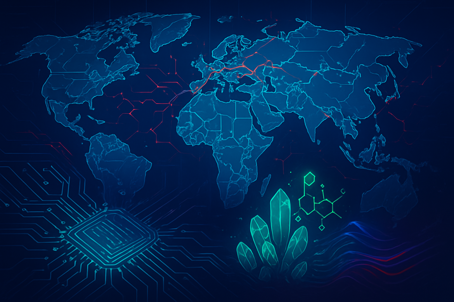
The Technical Chessboard: DUV Lithography Meets Rare Earth Dominance
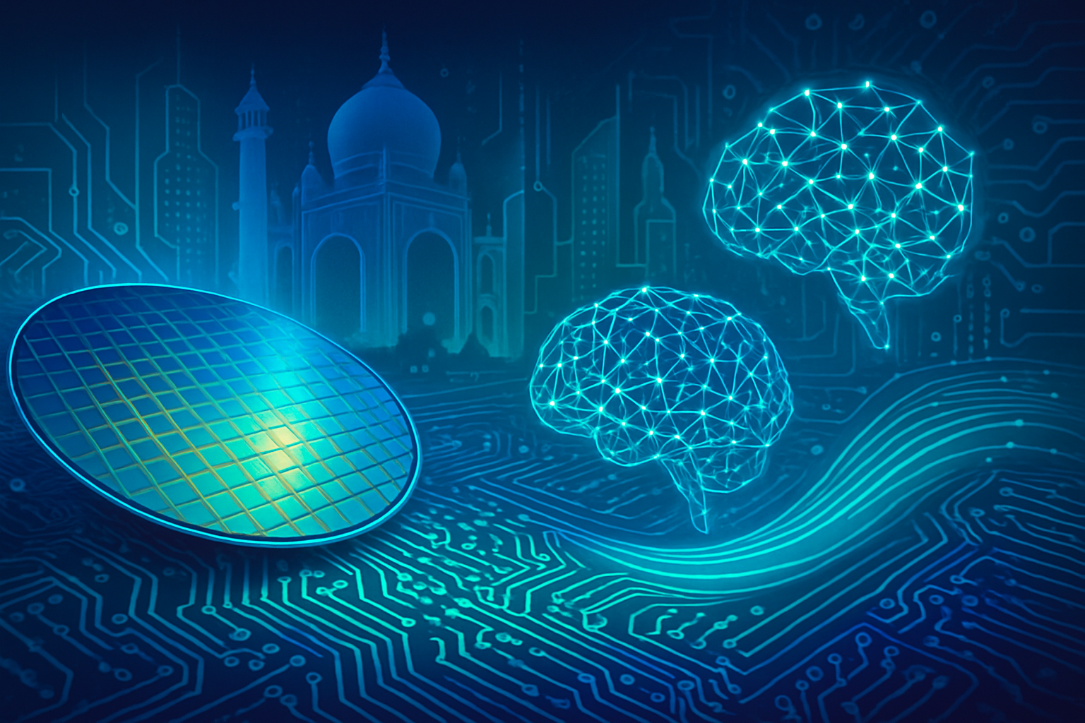
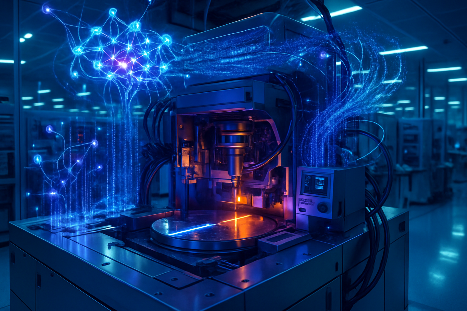
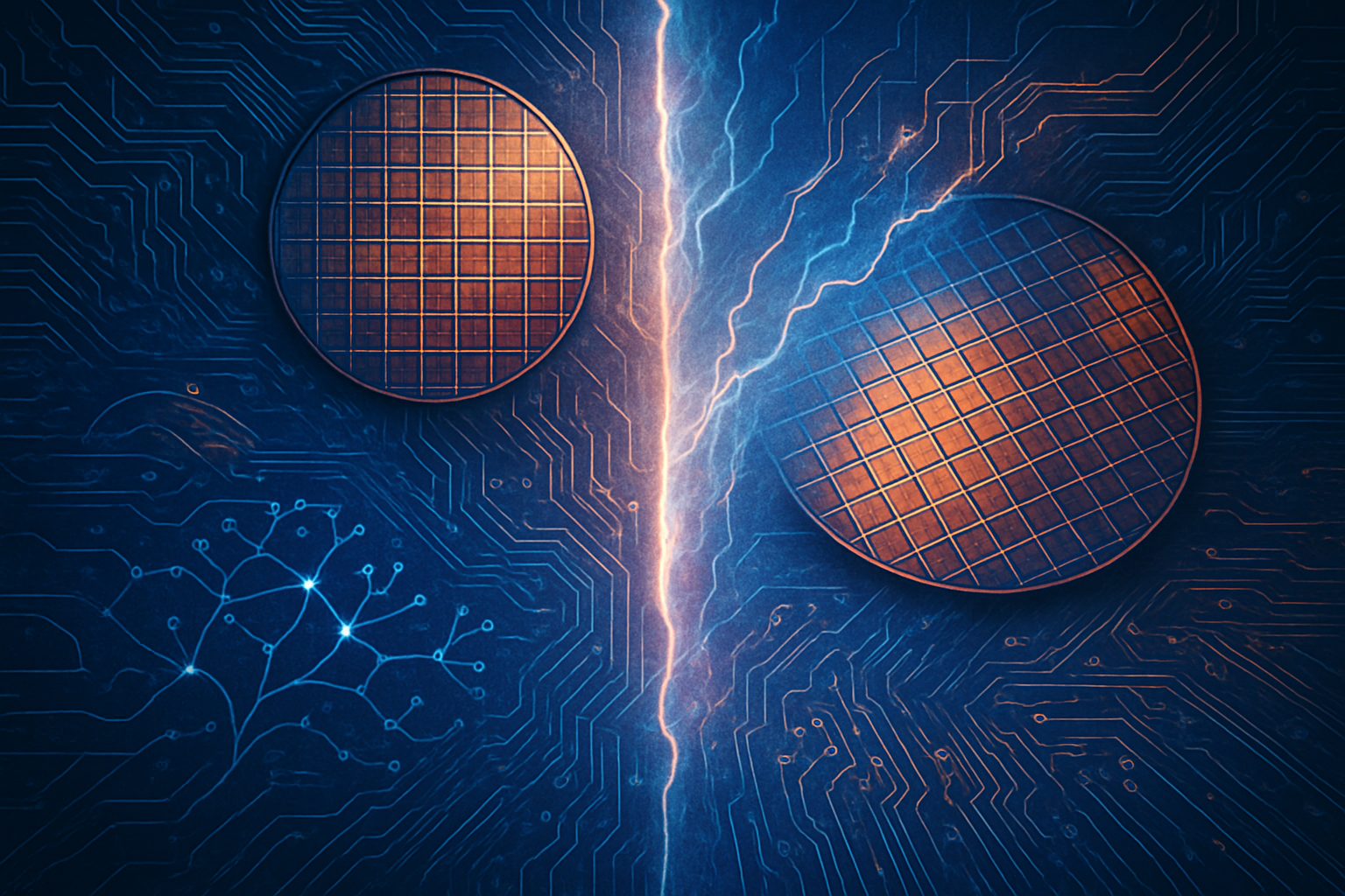
The core of this escalating trade dispute lies in two highly specialized and strategically vital technological domains: DUV lithography and rare earth elements. Deep Ultraviolet (DUV) lithography is the workhorse of the semiconductor industry, employing deep ultraviolet light (typically 193 nm) to print intricate circuit patterns onto silicon wafers. While Extreme Ultraviolet (EUV) lithography is used for the most cutting-edge chips (7nm and below), DUV technology remains indispensable for manufacturing over 95% of chip layers globally, powering everything from smartphone touchscreens and memory chips to automotive navigation systems. The Netherlands-based ASML Holding N.V. (AMS: ASML, NASDAQ: ASML) is the world's leading manufacturer of these sophisticated machines, and the Dutch government has already implemented national export restrictions on some advanced DUV technology to China since early 2023, largely in coordination with the United States. An EU-wide ban would solidify and expand such restrictions.
China, on the other hand, holds an overwhelming dominance in the global rare earth market, controlling approximately 70% of global rare earth mining and a staggering 90% of global rare earth processing. These 17 elements are crucial for a vast array of high-tech applications, including permanent magnets for electric vehicles and wind turbines, advanced electronics, and critical defense systems. Beijing's strategic tightening of export controls began in April 2025 with seven heavy rare earth elements. However, the situation escalated dramatically on October 9, 2025, when China's Ministry of Commerce and the General Administration of Customs announced comprehensive new measures, effective November 8, 2025. These expanded controls added five more rare earth elements (including holmium, erbium, and europium) and, crucially, extended restrictions to include processing equipment and associated technologies. Furthermore, new "foreign direct product" rules, mirroring US regulations, are set to take effect on December 1, 2025, allowing China to restrict products made abroad using Chinese rare earth materials or technologies. This represents a strategic shift from volume-based restrictions to "capability-based controls," aimed at preserving China's technological lead in the rare earth value chain.
The proposed EU DUV ban would be a direct, reciprocal response to China's "capability-based controls." While China targets the foundational materials and processing knowledge for high-tech manufacturing, the EU would target the foundational equipment necessary for China to produce a wide range of essential semiconductors. This differs significantly from previous trade disputes, as it directly attacks the technological underpinnings of industrial capacity, rather than just finished goods or raw materials. Initial reactions from policy circles suggest a strong sentiment within the EU that such a measure, though drastic, might be necessary to demonstrate resolve and counter China's economic coercion.
Competitive Implications Across the Tech Spectrum
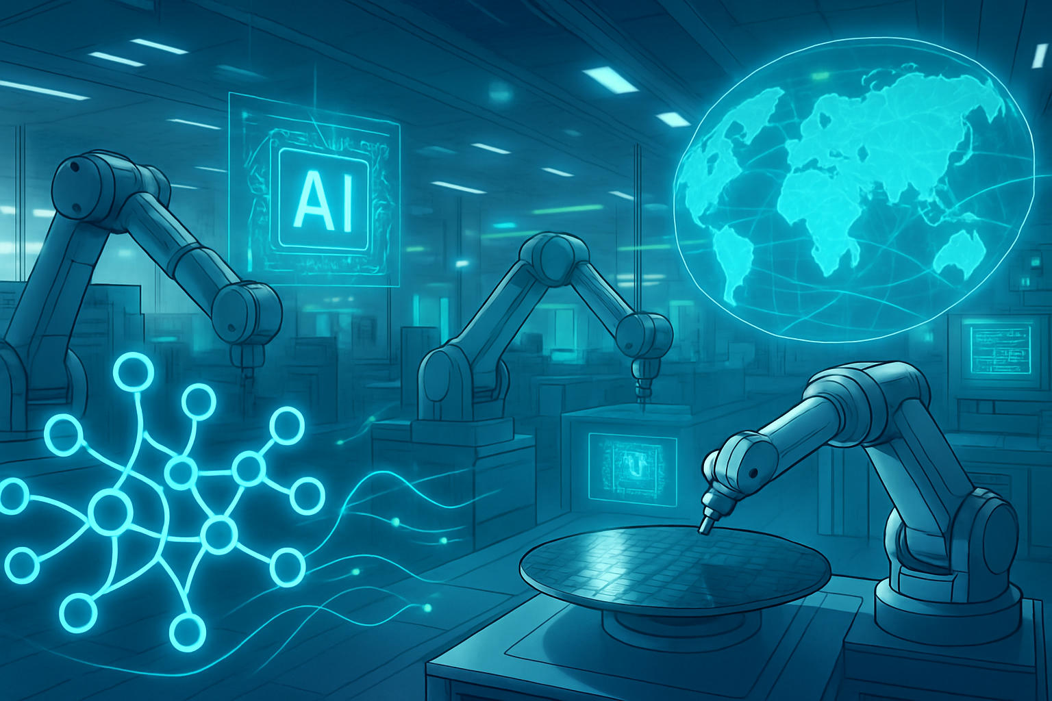
The ripple effects of such a trade conflict would be felt across the entire technology ecosystem, impacting established tech giants, semiconductor manufacturers, and emerging startups alike. For ASML Holding N.V. (AMS: ASML, NASDAQ: ASML), the world's sole producer of EUV and a major producer of DUV lithography systems, an EU-wide ban would further solidify existing restrictions on its sales to China, potentially impacting its revenue streams from the Chinese market, though it would also align with broader Western efforts to control advanced technology exports. Chinese semiconductor foundries, such as Semiconductor Manufacturing International Corporation (HKG: 0981, SSE: 688046), would face significant challenges in expanding or even maintaining their mature node production capabilities without access to new DUV machines, hindering their ambition for self-sufficiency.
On the other side, European industries heavily reliant on rare earths – including automotive manufacturers transitioning to electric vehicles, renewable energy companies building wind turbines, and defense contractors – would face severe supply chain disruptions, production delays, and increased costs. While the immediate beneficiaries of such a ban might be non-Chinese rare earth processing companies or alternative DUV equipment manufacturers (if any could scale up quickly), the broader impact is likely to be negative for global trade and economic efficiency. US tech giants, while not directly targeted by the EU's DUV ban, would experience indirect impacts through global supply chain instability, potential increases in chip prices, and a more fragmented global market.
This situation forces companies to re-evaluate their global supply chain strategies, accelerating trends towards "de-risking" and diversification away from single-country dependencies. Market positioning will increasingly be defined by access to critical resources and foundational technologies, potentially leading to significant investment in domestic or allied production capabilities for both rare earths and semiconductors. Startups and smaller innovators, particularly those in hardware development, could face higher barriers to entry due to increased component costs and supply chain uncertainties.
A Defining Moment in the Broader AI Landscape
While not directly an AI advancement, this geopolitical struggle over DUV machines and rare earths has profound implications for the broader AI landscape. AI development, from cutting-edge research to deployment in various applications, is fundamentally dependent on hardware – the chips, sensors, and power systems that rely on both advanced and mature node semiconductors, and often incorporate rare earth elements. Restrictions on DUV machines could slow China's ability to produce essential chips for AI accelerators, edge AI devices, and the vast data centers that fuel AI development. Conversely, rare earth controls impact the magnets in advanced robotics, drones, and other AI-powered physical systems, as well as the manufacturing processes for many electronic components.
This scenario fits into a broader trend of technological nationalism and the weaponization of economic dependencies. It highlights the growing recognition that control over foundational technologies and critical raw materials is paramount for national security and economic competitiveness in the age of AI. The potential concerns are widespread: economic decoupling could lead to less efficient global innovation, higher costs for consumers, and a slower pace of technological advancement in affected sectors. There's also the underlying concern that such controls could impact military applications, as both DUV machines and rare earths are vital for defense technologies.
Comparing this to previous AI milestones, this event signifies a shift from celebrating breakthroughs in algorithms and models to grappling with the geopolitical realities of their underlying hardware infrastructure. It underscores that the "AI race" is not just about who has the best algorithms, but who controls the means of production for the chips and components that power them. This is a critical juncture where supply chain resilience and strategic autonomy become as important as computational power and data access for national AI strategies.
The Path Ahead: Diplomacy, Diversification, and Disruption
The coming weeks and months will be crucial in determining the trajectory of this escalating tech rivalry. Near-term developments will center on the outcomes of diplomatic engagements between the EU and China. EU Trade Commissioner Maroš Šefčovič has invited Chinese Commerce Minister Wang Wentao to Brussels for face-to-face negotiations following a "constructive" video call in October 2025. The effectiveness of China's new rare earth export controls, which become effective on November 8, 2025, and their extraterritorial "foreign direct product" rules on December 1, 2025, will also be closely watched. The EU's formal decision regarding the DUV export ban, and whether it materializes as a collective measure or remains a national prerogative like the Netherlands', will be a defining moment.
In the long term, experts predict a sustained push towards diversification of rare earth supply chains, with significant investments in mining and processing outside China, particularly in North America, Australia, and Europe. Similarly, efforts to onshore or "friend-shore" semiconductor manufacturing will accelerate, with initiatives like the EU Chips Act and the US CHIPS Act gaining renewed urgency. However, these efforts face immense challenges, including the high cost and environmental impact of establishing new rare earth processing facilities, and the complexity and capital intensity of building advanced semiconductor fabs. What experts predict is a more fragmented global tech ecosystem, where supply chains are increasingly bifurcated along geopolitical lines, leading to higher production costs and potentially slower innovation in certain areas.
Potential applications and use cases on the horizon might include new material science breakthroughs to reduce reliance on specific rare earths, or advanced manufacturing techniques that require less sophisticated lithography. However, the immediate future is more likely to be dominated by efforts to secure existing supply chains and mitigate risks.
A Critical Juncture in AI's Global Fabric
In summary, the EU's consideration of a DUV machine export ban in response to China's rare earth controls represents a profound and potentially irreversible shift in global trade and technology policy. This development underscores the escalating tech rivalry between major powers, where critical resources and foundational manufacturing capabilities are increasingly weaponized as instruments of geopolitical leverage. The implications are severe, threatening to fragment global supply chains, increase costs, and reshape international relations for decades to come.
This moment will be remembered as a critical juncture in AI history, not for a breakthrough in AI itself, but for defining the geopolitical and industrial landscape upon which future AI advancements will depend. It highlights the vulnerability of a globally interconnected technological ecosystem to strategic competition and the urgent need for nations to balance interdependence with strategic autonomy. What to watch for in the coming weeks and months are the outcomes of the diplomatic negotiations, the practical enforcement and impact of China's rare earth controls, and the EU's ultimate decision regarding DUV export restrictions. These actions will set the stage for the future of global technology and the trajectory of AI development.
This content is intended for informational purposes only and represents analysis of current AI developments.
TokenRing AI delivers enterprise-grade solutions for multi-agent AI workflow orchestration, AI-powered development tools, and seamless remote collaboration platforms.
For more information, visit https://www.tokenring.ai/.