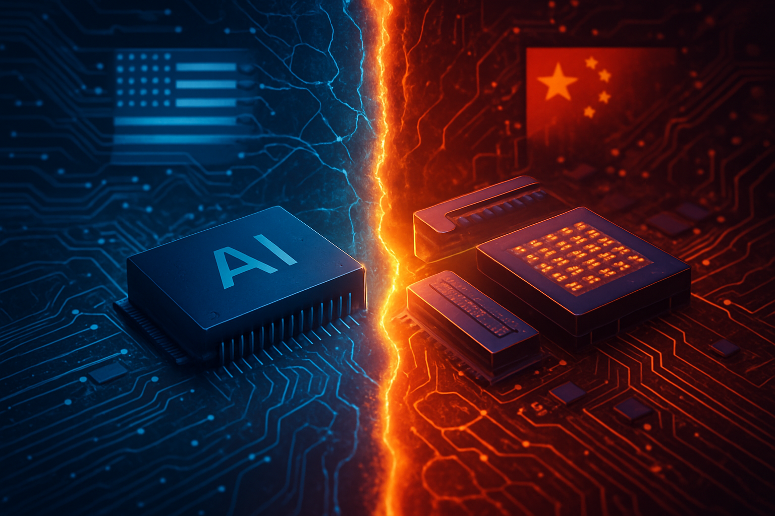
The semiconductor industry is at the precipice of a fundamental and irreversible transformation, driven not just by the demand for Artificial Intelligence (AI) but by AI itself. This profound shift is ushering in the era of "AI-era silicon," where AI is becoming both the ultimate consumer of advanced chips and the architect of their creation. This symbiotic relationship is accelerating innovation across every stage of the semiconductor lifecycle, from initial design and materials discovery to advanced manufacturing and packaging. The immediate significance is the creation of next-generation chips that are faster, more energy-efficient, and highly specialized, tailored precisely for the insatiable demands of advanced AI applications like generative AI, large language models (LLMs), and autonomous systems. This isn't merely an incremental improvement; it's a paradigm shift that promises to redefine the limits of computational power and efficiency.
Technical Deep Dive: AI Forging the Future of Chips
The integration of AI into semiconductor design and manufacturing marks a radical departure from traditional methodologies, largely replacing human-intensive, iterative processes with autonomous, data-driven optimization. This technical revolution is spearheaded by leading Electronic Design Automation (EDA) companies and tech giants, leveraging sophisticated AI techniques, particularly reinforcement learning and generative AI, to tackle the escalating complexity of modern chip architectures.
Google's pioneering AlphaChip exemplifies this shift. Utilizing a reinforcement learning (RL) model, AlphaChip addresses the notoriously complex and time-consuming task of chip floorplanning. Floorplanning, the arrangement of components on a silicon die, significantly impacts a chip's power consumption and speed. AlphaChip treats this as a game, iteratively placing components and learning from the outcomes. Its core innovation lies in an edge-based graph neural network (Edge-GNN), which understands the intricate relationships and interconnections between chip components. This allows it to generate high-quality floorplans in under six hours, a task that traditionally took human engineers months. AlphaChip has been instrumental in designing the last three generations of Google's (NASDAQ: GOOGL) custom AI accelerators, the Tensor Processing Unit (TPU), including the latest Trillium (6th generation), and Google Axion Processors. While initial claims faced some scrutiny regarding comparison methodologies, AlphaChip remains a landmark application of RL to real-world engineering.
Similarly, Cadence's (NASDAQ: CDNS) Cerebrus, part of its Cadence.AI portfolio, employs a unique reinforcement learning engine to automate and scale digital chip design across the entire RTL-to-signoff implementation flow. Cerebrus focuses on optimizing Power, Performance, and Area (PPA) and boasts up to 20% better PPA and a 10X improvement in engineering productivity. Its latest iteration, Cadence Cerebrus AI Studio, introduces "agentic AI" workflows, where autonomous AI agents orchestrate entire design optimization methodologies for multi-block, multi-user SoC designs. This moves beyond assisting engineers to having AI manage complex, holistic design processes. Customers like MediaTek (TWSE: 2454) have reported significant die area and power reductions using Cerebrus, validating its real-world impact.
Not to be outdone, Synopsys (NASDAQ: SNPS) offers a comprehensive suite of AI-driven EDA solutions under Synopsys.ai. Its flagship, DSO.ai (Design Space Optimization AI), launched in 2020, uses reinforcement learning to autonomously search for optimization targets in vast solution spaces, achieving superior PPA with reported power reductions of up to 15% and significant die size reductions. DSO.ai has been used in over 200 commercial chip tape-outs. Beyond design, Synopsys.ai extends to VSO.ai (Verification Space Optimization AI) for faster functional testing and TSO.ai (Test Space Optimization AI) for manufacturing test optimization. More recently, Synopsys introduced Synopsys.ai Copilot, leveraging generative AI to streamline tasks like documentation searches and script generation, boosting engineer productivity by up to 30%. The company is also developing "AgentEngineer" technology for higher levels of autonomous execution. These tools collectively transform the design workflow from manual iteration to autonomous, data-driven optimization, drastically reducing time-to-market and improving chip quality.
Industry Impact: Reshaping the Competitive Landscape
The advent of AI-era silicon is not just a technological marvel; it's a seismic event reshaping the competitive dynamics of the entire tech industry, creating clear winners and posing significant challenges.
NVIDIA (NASDAQ: NVDA) stands as a colossal beneficiary, its market capitalization surging due to its dominant GPU architecture and the ubiquitous CUDA software ecosystem. Its chips are the backbone of AI training and inference, offering unparalleled parallel processing capabilities. NVIDIA's new Blackwell GPU architecture and GB200 Grace Blackwell Superchip are poised to further extend its lead. Intel (NASDAQ: INTC) is strategically pivoting, developing new data center GPUs like "Crescent Island" and leveraging Intel Foundry Services (IFS) to manufacture chips for others, including Microsoft's (NASDAQ: MSFT) Maia 2 AI accelerator. This shift aims to regain lost ground in the AI chip market. AMD (NASDAQ: AMD) is aggressively challenging NVIDIA with its Instinct GPUs (e.g., MI300 series), gaining traction with hyperscalers, and powering AI in Copilot PCs with its Ryzen AI Pro 300 series.
EDA leaders Synopsys and Cadence are solidifying their positions by embedding AI across their product portfolios. Their AI-driven tools are becoming indispensable, offering "full-stack AI-driven EDA solutions" that enable chip designers to manage increasing complexity, automate tasks, and achieve superior quality faster. For foundries like TSMC (NYSE: TSM), AI is critical for both internal operations and external demand. TSMC uses AI to boost energy efficiency, classify wafer defects, and implement predictive maintenance, improving yield and reducing downtime. It manufactures virtually all high-performance AI chips and anticipates substantial revenue growth from AI-specific chips, reinforcing its competitive edge.
Major AI labs and tech giants like Google, Meta (NASDAQ: META), Microsoft, and Amazon (NASDAQ: AMZN) are increasingly designing their own custom AI chips (ASICs) to optimize performance, efficiency, and cost for their specific AI workloads, reducing reliance on external suppliers. This "insourcing" of chip design creates both opportunities for collaboration with foundries and competitive pressure for traditional chipmakers. The disruption extends to time-to-market, which is dramatically accelerated by AI, and the potential democratization of chip design as AI tools make complex tasks more accessible. Emerging trends like rectangular panel-level packaging for larger AI chips could even disrupt traditional round silicon wafer production, creating new supply chain ecosystems.
Wider Significance: A Foundational Shift for AI Itself
The integration of AI into semiconductor design and manufacturing is not just about making better chips; it's about fundamentally altering the trajectory of AI development itself. This represents a profound milestone, distinct from previous AI breakthroughs.
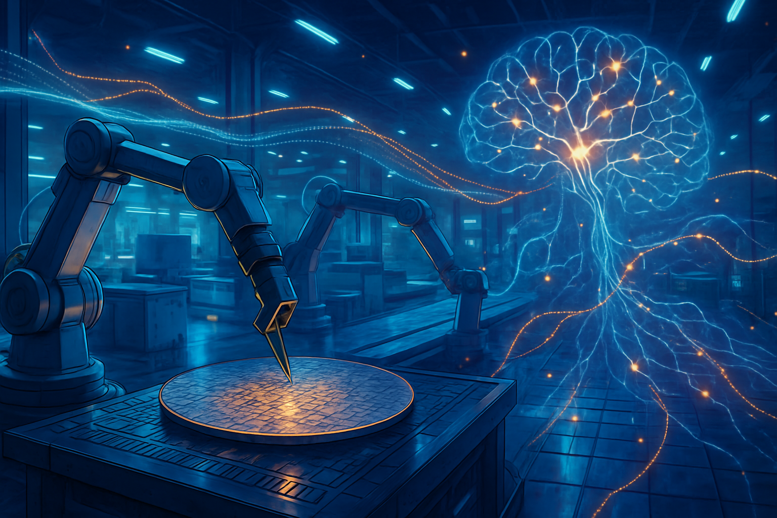
This era is characterized by a symbiotic relationship where AI acts as a "co-creator" in the chip lifecycle, optimizing every aspect from design to manufacturing. This creates a powerful feedback loop: AI designs better chips, which then power more advanced AI, demanding even more sophisticated hardware, and so on. This self-accelerating cycle is crucial for pushing the boundaries of what AI can achieve. As traditional scaling challenges Moore's Law, AI-driven innovation in design, advanced packaging (like 3D integration), heterogeneous computing, and new materials offers alternative pathways for continued performance gains, ensuring the computational resources for future AI breakthroughs remain viable.
The shift also underpins the growing trend of Edge AI and decentralization, moving AI processing from centralized clouds to local devices. This paradigm, driven by the need for real-time decision-making, reduced latency, and enhanced privacy, relies heavily on specialized, energy-efficient AI-era silicon. This marks a maturation of AI, moving towards a hybrid ecosystem of centralized and distributed computing, enabling intelligence to be pervasive and embedded in everyday devices.
However, this transformative era is not without its concerns. Job displacement due to automation is a significant worry, though experts suggest AI will more likely augment engineers in the near term, necessitating widespread reskilling. The inherent complexity of integrating AI into already intricate chip design processes, coupled with the exorbitant costs of advanced fabs and AI infrastructure, could concentrate power among a few large players. Ethical considerations, such as algorithmic bias and the "black box" nature of some AI decisions, also demand careful attention. Furthermore, the immense computational power required by AI workloads and manufacturing processes raises concerns about energy consumption and environmental impact, pushing for innovations in sustainable practices.
Future Developments: The Road Ahead for Intelligent Silicon
The future of AI-driven semiconductor design and manufacturing promises a continuous cascade of innovations, pushing the boundaries of what's possible in computing.
In the near term (1-3 years), we can expect further acceleration of design cycles through more sophisticated AI-powered EDA tools that automate layout, simulation, and code generation. Enhanced defect detection and quality control will see AI-driven visual inspection systems achieve even higher accuracy, often surpassing human capabilities. Predictive maintenance, leveraging AI to analyze sensor data, will become standard, reducing unplanned downtime by up to 50%. Real-time process optimization and yield optimization will see AI dynamically adjusting manufacturing parameters to ensure uniform film thickness, reduce micro-defects, and maximize throughput. Generative AI will increasingly streamline workflows, from eliminating waste to speeding design iterations and assisting workers with real-time adjustments.
Looking to the long term (3+ years), the vision is one of autonomous semiconductor manufacturing, with "self-healing fabs" where machines detect and resolve issues with minimal human intervention, combining AI with IoT and digital twins. A profound development will be AI designing AI chips, creating a virtuous cycle where AI tools continuously improve their ability to design even more advanced hardware, potentially leading to the discovery of new materials and architectures. The pursuit of smaller process nodes (2nm and beyond) will continue, alongside extensive research into 2D materials, ferroelectrics, and neuromorphic designs that mimic the human brain. Heterogeneous integration and advanced packaging (3D integration, chiplets) will become standard to minimize data travel and reduce power consumption in high-performance AI systems. Explainable AI (XAI) will also become crucial to demystify "black-box" models, enabling better interpretability and validation.
Potential applications on the horizon are vast, from generative design where natural-language specifications translate directly into Verilog code ("ChipGPT"), to AI auto-generating testbenches and assertions for verification. In manufacturing, AI will enable smart testing, predicting chip failures at the wafer sort stage, and optimizing supply chain logistics through real-time demand forecasting. Challenges remain, including data scarcity, the interpretability of AI models, a persistent talent gap, and the high costs associated with advanced fabs and AI integration. Experts predict an "AI supercycle" for at least the next five to ten years, with the global AI chip market projected to surpass $150 billion in 2025 and potentially reach $1.3 trillion by 2030. The industry will increasingly focus on heterogeneous integration, AI designing its own hardware, and a strong emphasis on sustainability.
Comprehensive Wrap-up: Forging the Future of Intelligence
The convergence of AI and the semiconductor industry represents a pivotal transformation, fundamentally reshaping how microchips are conceived, designed, manufactured, and utilized. This "AI-era silicon" is not merely a consequence of AI's advancements but an active enabler, creating a symbiotic relationship that propels both fields forward at an unprecedented pace.
Key takeaways highlight AI's pervasive influence: accelerating chip design through automated EDA tools, optimizing manufacturing with predictive maintenance and defect detection, enhancing supply chain resilience, and driving the emergence of specialized AI chips. This development signifies a foundational shift in AI history, creating a powerful virtuous cycle where AI designs better chips, which in turn enable more sophisticated AI models. It's a critical pathway for pushing beyond traditional Moore's Law scaling, ensuring that the computational resources for future AI breakthroughs remain viable.
The long-term impact promises a future of abundant, specialized, and energy-efficient computing, unlocking entirely new applications across diverse fields from drug discovery to autonomous systems. This will reshape economic landscapes and intensify competitive dynamics, necessitating unprecedented levels of industry collaboration, especially in advanced packaging and chiplet-based architectures.
In the coming weeks and months, watch for continued announcements from major foundries regarding AI-driven yield improvements, the commercialization of new AI-powered manufacturing and EDA tools, and the unveiling of innovative, highly specialized AI chip designs. Pay attention to the deeper integration of AI into mainstream consumer devices and further breakthroughs in design-technology co-optimization (DTCO) and advanced packaging. The synergy between AI and semiconductor technology is forging a new era of computational capability, promising to unlock unprecedented advancements across nearly every technological frontier. The journey ahead will be characterized by rapid innovation, intense competition, and a transformative impact on our digital world.
This content is intended for informational purposes only and represents analysis of current AI developments.
TokenRing AI delivers enterprise-grade solutions for multi-agent AI workflow orchestration, AI-powered development tools, and seamless remote collaboration platforms.
For more information, visit https://www.tokenring.ai/.