The unprecedented demand for artificial intelligence (AI) capabilities is driving a profound and rapid transformation in semiconductor technology. This isn't merely an incremental evolution but a fundamental shift in how chips are designed, manufactured, and integrated, directly addressing the immense computational hunger and power efficiency requirements of modern AI workloads, particularly those underpinning generative AI and large language models (LLMs). The innovations span specialized architectures, advanced packaging, and revolutionary memory solutions, collectively forming the bedrock upon which the current AI megatrend is being built. Without these continuous breakthroughs in silicon, the scaling and performance of today's most sophisticated AI applications would be severely constrained, making the semiconductor industry the silent, yet most crucial, enabler of the AI revolution.
The Silicon Engine of Progress: Unpacking AI's Hardware Revolution
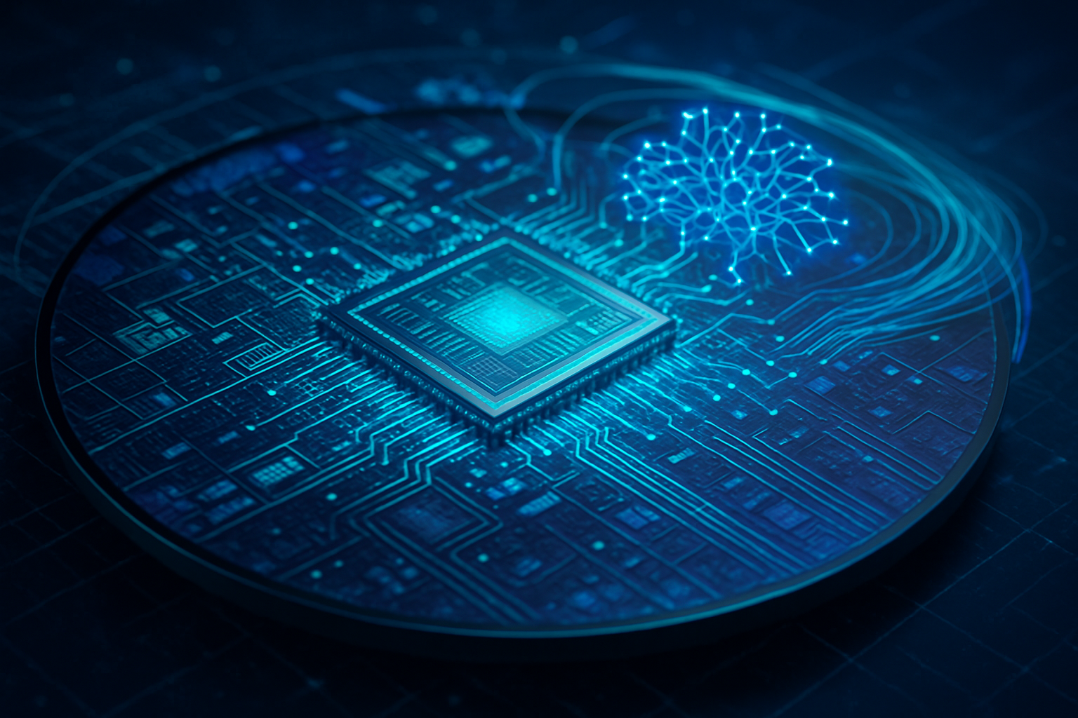
The core of AI's current capabilities lies in a series of groundbreaking advancements across chip design, production, and memory technologies, each offering significant departures from previous, more general-purpose computing paradigms. These innovations prioritize specialized processing, enhanced data throughput, and vastly improved power efficiency.
In chip design, Graphics Processing Units (GPUs) from companies like NVIDIA (NVDA) have evolved far beyond their original graphics rendering purpose. A pivotal advancement is the integration of Tensor Cores, first introduced by NVIDIA in its Volta architecture in 2017. These specialized hardware units are purpose-built to accelerate mixed-precision matrix multiplication and accumulation operations, which are the mathematical bedrock of deep learning. Unlike traditional GPU cores, Tensor Cores efficiently handle lower-precision inputs (e.g., FP16) and accumulate results in higher precision (e.g., FP32), leading to substantial speedups—up to 20 times faster than FP32-based matrix multiplication—with minimal accuracy loss for AI tasks. This, coupled with the massively parallel architecture of thousands of simpler processing cores (like NVIDIA’s CUDA cores), allows GPUs to execute numerous calculations simultaneously, a stark contrast to the fewer, more complex sequential processing cores of Central Processing Units (CPUs).
Application-Specific Integrated Circuits (ASICs) represent another critical leap. These are custom-designed chips meticulously engineered for particular AI workloads, offering extreme performance and efficiency for their intended functions. Google (GOOGL), for example, developed its Tensor Processing Units (TPUs) as ASICs optimized for the matrix operations that dominate deep learning inference. While ASICs deliver unparalleled performance and superior power efficiency for their specialized tasks by eliminating unnecessary general-purpose circuitry, their fixed-function nature means they are less adaptable to rapidly evolving AI algorithms or new model architectures, unlike programmable GPUs.
Even more radically, Neuromorphic Chips are emerging, inspired by the energy-efficient, parallel processing of the human brain. These chips, like IBM's TrueNorth and Intel's (INTC) Loihi, employ physical artificial neurons and synaptic connections to process information in an event-driven, highly parallel manner, mimicking biological neural networks. They operate on discrete "spikes" rather than continuous clock cycles, leading to significant energy savings. This fundamentally departs from the traditional Von Neumann architecture, which suffers from the "memory wall" bottleneck caused by constant data transfer between separate processing and memory units. Neuromorphic chips address this by co-locating memory and computation, resulting in extremely low power consumption (e.g., 15-300mW compared to 250W+ for GPUs in some tasks) and inherent parallelism, making them ideal for real-time edge AI in robotics and autonomous systems.
Production advancements are equally crucial. Advanced packaging integrates multiple semiconductor components into a single, compact unit, surpassing the limitations of traditional monolithic die packaging. Techniques like 2.5D Integration, where multiple dies (e.g., logic and High Bandwidth Memory, HBM) are placed side-by-side on a silicon interposer with high-density interconnects, are exemplified by NVIDIA’s H100 GPUs. This creates an ultra-wide, short communication bus, effectively mitigating the "memory wall." 3D Integration (3D ICs) stacks dies vertically, interconnected by Through-Silicon Vias (TSVs), enabling ultrafast signal transfer and reduced power consumption. The rise of chiplets—pre-fabricated, smaller functional blocks integrated into a single package—offers modularity, allowing different parts of a chip to be fabricated on their most suitable process nodes, reducing costs and increasing design flexibility. These methods enable much closer physical proximity between components, resulting in significantly shorter interconnects, higher bandwidth, and better power integrity, thus overcoming physical scaling limitations that traditional packaging could not address.
Extreme Ultraviolet (EUV) lithography is a pivotal enabling technology for manufacturing these cutting-edge chips. EUV employs light with an extremely short wavelength (13.5 nanometers) to project intricate circuit patterns onto silicon wafers with unprecedented precision, enabling the fabrication of features down to a few nanometers (sub-7nm, 5nm, 3nm, and beyond). This is critical for achieving higher transistor density, translating directly into more powerful and energy-efficient AI processors and extending the viability of Moore's Law.
Finally, memory technologies have seen revolutionary changes. High Bandwidth Memory (HBM) is an advanced type of DRAM specifically engineered for extremely high-speed data transfer with reduced power consumption. HBM uses a 3D stacking architecture where multiple memory dies are vertically stacked and interconnected via TSVs, creating an exceptionally wide I/O interface (typically 1024-bit wide per stack). HBM3, for instance, can reach up to 3 TB/s, vastly outperforming traditional DDR memory (DDR5 offers approximately 33.6 GB/s). This immense bandwidth and reduced latency are indispensable for AI workloads that demand rapid data access, such as training large language models.
In-Memory Computing (PIM) is another paradigm shift, designed to overcome the "Von Neumann bottleneck" by integrating processing elements directly within or very close to the memory subsystem. By performing computations directly where the data resides, PIM minimizes the energy expenditure and time delays associated with moving large volumes of data between separate processing units and memory. This significantly enhances energy efficiency and accelerates AI inference, particularly for memory-intensive computing systems, by drastically reducing data transfers.
Reshaping the AI Industry: Corporate Battles and Strategic Plays
The relentless innovation in AI semiconductors is profoundly reshaping the technology industry, creating significant competitive implications and strategic advantages while also posing potential disruptions. Companies at every layer of the tech stack are either benefiting from or actively contributing to this hardware revolution.
NVIDIA (NVDA) remains the undisputed leader in the AI GPU market, commanding an estimated 80-85% market share. Its comprehensive CUDA ecosystem and continuous innovation with architectures like Hopper and the upcoming Blackwell solidify its leadership, making its GPUs indispensable for major tech companies and AI labs for training and deploying large-scale AI models. This dominance, however, has spurred other tech giants to invest heavily in developing custom silicon to reduce their dependence, igniting an "AI Chip Race" that fosters greater vertical integration across the industry.
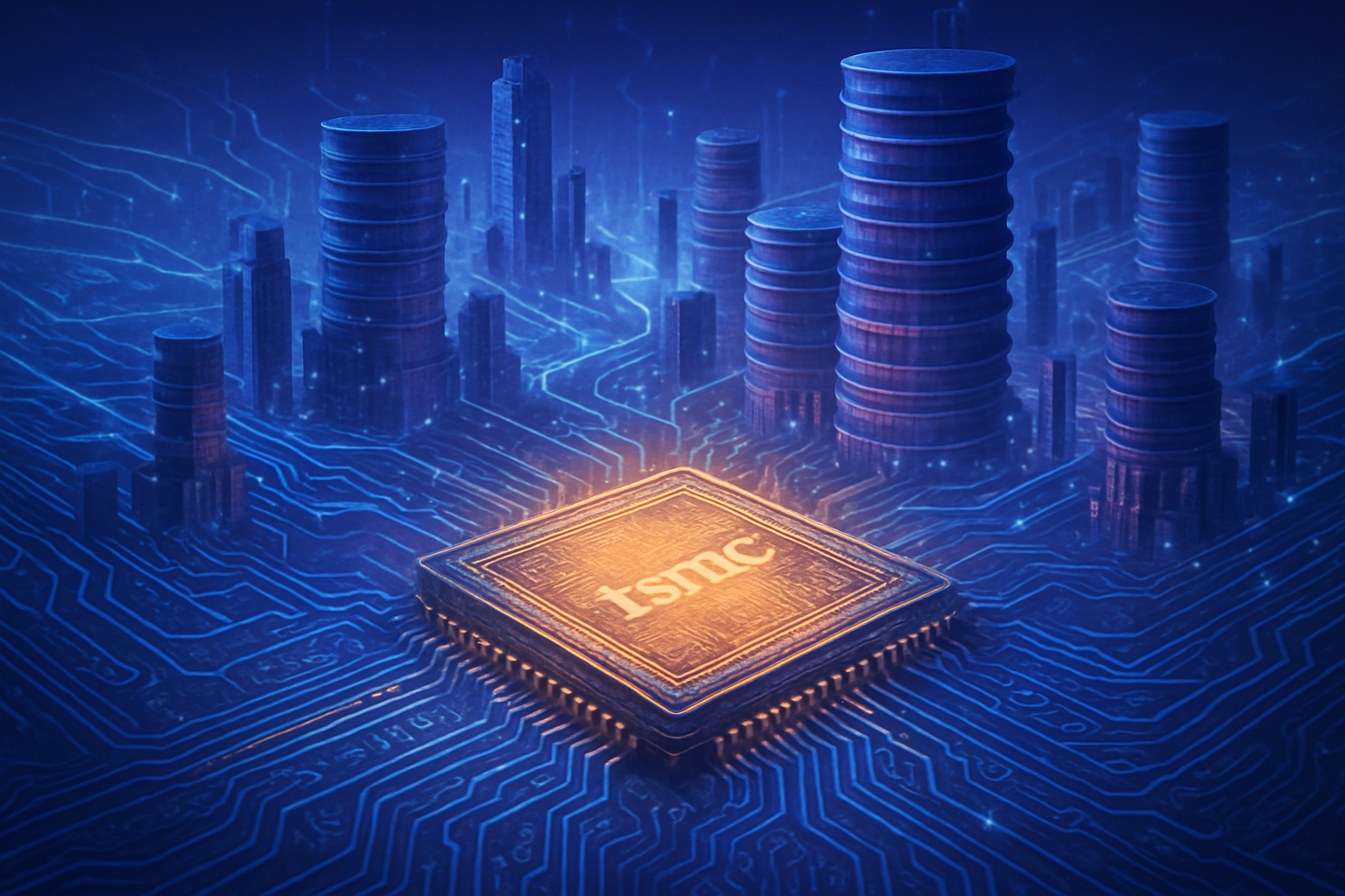
TSMC (Taiwan Semiconductor Manufacturing Company) (TSM) stands as an indispensable player. As the world's leading pure-play foundry, its ability to fabricate cutting-edge AI chips using advanced process nodes (e.g., 3nm, 2nm) and packaging technologies (e.g., CoWoS) at scale directly impacts the performance and cost-efficiency of nearly every advanced AI product, including those from NVIDIA and AMD. TSMC anticipates its AI-related revenue to grow at a compound annual rate of 40% through 2029, underscoring its pivotal role.
Other key beneficiaries and contenders include AMD (Advanced Micro Devices) (AMD), a strong competitor to NVIDIA, developing powerful processors and AI-powered chips for various segments. Intel (INTC), while facing stiff competition, is aggressively pushing to regain leadership in advanced manufacturing processes (e.g., 18A nodes) and integrating AI acceleration into its Xeon Scalable processors. Tech giants like Google (GOOGL) with its TPUs (e.g., Trillium), Amazon (AMZN) with Trainium and Inferentia chips for AWS, and Microsoft (MSFT) with its Maia and Cobalt custom silicon, are all designing their own chips optimized for their specific AI workloads, strengthening their cloud offerings and reducing reliance on third-party hardware. Apple (AAPL) integrates its own Neural Engine Units (NPUs) into its devices, optimizing for on-device machine learning tasks. Furthermore, specialized companies like ASML (ASML), providing critical EUV lithography equipment, and EDA (Electronic Design Automation) vendors like Synopsys, whose AI-driven tools are now accelerating chip design cycles, are crucial enablers.
The competitive landscape is marked by both consolidation and unprecedented innovation. The immense cost and complexity of advanced chip manufacturing could lead to further concentration of value among a handful of top players. However, AI itself is paradoxically lowering barriers to entry in chip design. Cloud-based, AI-augmented design tools allow nimble startups to access advanced resources without substantial upfront infrastructure investments, democratizing chip development and accelerating production. Companies like Groq, excelling in high-performance AI inference chips, exemplify this trend.
Potential disruptions include the rapid obsolescence of older hardware due to the adoption of new manufacturing processes, a structural shift from CPU-centric to parallel processing architectures, and a projected shortage of one million skilled workers in the semiconductor industry by 2030. The insatiable demand for high-performance chips also strains global production capacity, leading to rolling shortages and inflated prices. However, strategic advantages abound: AI-driven design tools are compressing development cycles, machine learning optimizes chips for greater performance and energy efficiency, and new business opportunities are unlocking across the entire semiconductor value chain.
Beyond the Transistor: Wider Implications for AI and Society
The pervasive integration of AI, powered by these advanced semiconductors, extends far beyond mere technological enhancement; it is fundamentally redefining AI’s capabilities and its role in society. This innovation is not just making existing AI faster; it is enabling entirely new applications previously considered science fiction, from real-time language processing and advanced robotics to personalized healthcare and autonomous systems.
This era marks a significant shift from AI primarily consuming computational power to AI actively contributing to its own foundation. AI-driven Electronic Design Automation (EDA) tools automate complex chip design tasks, compress development timelines, and optimize for power, performance, and area (PPA). In manufacturing, AI uses predictive analytics, machine learning, and computer vision to optimize yield, reduce defects, and enhance equipment uptime. This creates an "AI supercycle" where advancements in AI fuel the demand for more sophisticated semiconductors, which, in turn, unlock new possibilities for AI itself, creating a self-improving technological ecosystem.
The societal impacts are profound. AI's reach now extends to virtually every sector, leading to sophisticated products and services that enhance daily life and drive economic growth. The global AI chip market is projected for substantial growth, indicating a profound economic impact and fueling a new wave of industrial automation. However, this technological shift also brings concerns about workforce disruption due to automation, particularly in labor-intensive tasks, necessitating proactive measures for retraining and new opportunities.
Ethical concerns are also paramount. The powerful AI hardware's ability to collect and analyze vast amounts of user data raises critical questions about privacy breaches and misuse. Algorithmic bias, embedded in training data, can be perpetuated or amplified, leading to discriminatory outcomes in areas like hiring or criminal justice. Security vulnerabilities in AI-powered devices and complex questions of accountability for autonomous systems also demand careful consideration and robust solutions.
Environmentally, the energy-intensive nature of large-scale AI models and data centers, coupled with the resource-intensive manufacturing of chips, raises concerns about carbon emissions and resource depletion. Innovations in energy-efficient designs, advanced cooling technologies, and renewable energy integration are critical to mitigate this impact. Geopolitically, the race for advanced semiconductor technology has reshaped global power dynamics, with countries vying for dominance in chip manufacturing and supply chains, leading to increased tensions and significant investments in domestic fabrication capabilities.
Compared to previous AI milestones, such as the advent of deep learning or the development of the first powerful GPUs, the current wave of semiconductor innovation represents a distinct maturation and industrialization of AI. It signifies AI’s transition from a consumer to an active creator of its own foundational hardware. Hardware is no longer a generic component but a strategic differentiator, meticulously engineered to unlock the full potential of AI algorithms. This "hand in glove" architecture is accelerating the industrialization of AI, making it more robust, accessible, and deeply integrated into our daily lives and critical infrastructure.
The Road Ahead: Next-Gen Chips and Uncharted AI Frontiers
The trajectory of AI semiconductor technology promises continuous, transformative innovation, driven by the escalating demands of AI workloads. The near-term (1-3 years) will see a rapid transition to even smaller process nodes, with 3nm and 2nm technologies becoming prevalent. TSMC (TSM), for instance, anticipates high-volume production of its 2nm (N2) process node in late 2025, enabling higher transistor density crucial for complex AI models. Neural Processing Units (NPUs) are also expected to be widely integrated into consumer devices like smartphones and "AI PCs," with projections indicating AI PCs will comprise 43% of all PC shipments by late 2025. This will decentralize AI processing, reducing latency and cloud reliance. Furthermore, there will be a continued diversification and customization of AI chips, with ASICs optimized for specific workloads becoming more common, along with significant innovation in High-Bandwidth Memory (HBM) to address critical memory bottlenecks.
Looking further ahead (3+ years), the industry is poised for even more radical shifts. The widespread commercial integration of 2D materials like Indium Selenide (InSe) is anticipated beyond 2027, potentially ushering in a "post-silicon era" of ultra-efficient transistors. Neuromorphic computing, inspired by the human brain, will mature, offering unprecedented energy efficiency for AI tasks, particularly in edge and IoT applications. Experimental prototypes have already demonstrated real-time learning capabilities with minimal energy consumption. The integration of quantum computing with semiconductors promises unparalleled processing power for complex AI algorithms, with hybrid quantum-classical architectures emerging as a key area of development. Photonic AI chips, which use light for data transmission and computation, offer the potential for significantly greater energy efficiency and speed compared to traditional electronic systems. Breakthroughs in cryogenic CMOS technology will also address critical heat dissipation bottlenecks, particularly relevant for quantum computing.
These advancements will fuel a vast array of applications. In consumer electronics, AI chips will enhance features like advanced image and speech recognition and real-time decision-making. They are essential for autonomous systems (vehicles, drones, robotics) for real-time data processing at the edge. Data centers and cloud computing will leverage specialized AI accelerators for massive deep learning models and generative AI. Edge computing and IoT devices will benefit from local AI processing, reducing latency and enhancing privacy. Healthcare will see accelerated AI-powered diagnostics and drug discovery, while manufacturing and industrial automation will gain from optimized processes and predictive maintenance.
Despite this promising future, significant challenges remain. The high manufacturing costs and complexity of modern semiconductor fabrication plants, costing billions of dollars, create substantial barriers to entry. Heat dissipation and power consumption remain critical challenges for ever more powerful AI workloads. Memory bandwidth, despite HBM and PIM, continues to be a persistent bottleneck. Geopolitical risks, supply chain vulnerabilities, and a global shortage of skilled workers for advanced semiconductor tasks also pose considerable hurdles. Experts predict explosive market growth, with the global AI chip market potentially reaching $1.3 trillion by 2030. The future will likely be a heterogeneous computing environment, with intense diversification and customization of AI chips, and AI itself becoming the "backbone of innovation" within the semiconductor industry, transforming chip design, manufacturing, and supply chain management.
Powering the Future: A New Era for AI-Driven Innovation
The ongoing innovation in semiconductor technology is not merely supporting the AI megatrend; it is fundamentally powering and defining it. From specialized GPUs with Tensor Cores and custom ASICs to brain-inspired neuromorphic chips, and from advanced 2.5D/3D packaging to cutting-edge EUV lithography and high-bandwidth memory, each advancement builds upon the last, creating a virtuous cycle of computational prowess. These breakthroughs are dismantling the traditional bottlenecks of computing, enabling AI models to grow exponentially in complexity and capability, pushing the boundaries of what intelligent machines can achieve.
The significance of this development in AI history cannot be overstated. It marks a transition where hardware is no longer a generic component but a strategic differentiator, meticulously engineered to unlock the full potential of AI algorithms. This "hand in glove" architecture is accelerating the industrialization of AI, making it more robust, efficient, and deeply integrated into our daily lives and critical infrastructure.
As we look to the coming weeks and months, watch for continued announcements from major players like NVIDIA (NVDA), AMD (AMD), Intel (INTC), and TSMC (TSM) regarding next-generation chip architectures and manufacturing process nodes. Pay close attention to the increasing integration of NPUs in consumer devices and further developments in advanced packaging and memory solutions. The competitive landscape will intensify as tech giants continue to pursue custom silicon, and innovative startups emerge with specialized solutions. The challenges of cost, power consumption, and supply chain resilience will remain focal points, driving further innovation in materials science and manufacturing processes. The symbiotic relationship between AI and semiconductors is set to redefine the future of technology, creating an era of unprecedented intelligent capabilities.
This content is intended for informational purposes only and represents analysis of current AI developments.
TokenRing AI delivers enterprise-grade solutions for multi-agent AI workflow orchestration, AI-powered development tools, and seamless remote collaboration platforms.
For more information, visit https://www.tokenring.ai/.